 Datasheet下载
- 型号: BR24T02FVT-WE2
- 制造商: ROHM Semiconductor
- 库位|库存: xxxx|xxxx
- 要求:
| 数量阶梯 | 香港交货 | 国内含税 |
| +xxxx | $xxxx | ¥xxxx |
查看当月历史价格
查看今年历史价格
BR24T02FVT-WE2产品简介:
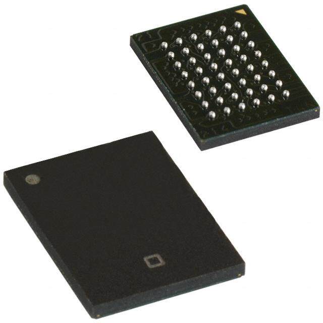
ICGOO电子元器件商城为您提供BR24T02FVT-WE2由ROHM Semiconductor设计生产,在icgoo商城现货销售,并且可以通过原厂、代理商等渠道进行代购。 BR24T02FVT-WE2价格参考¥2.93-¥3.32。ROHM SemiconductorBR24T02FVT-WE2封装/规格:存储器, EEPROM 存储器 IC 2Kb (256 x 8) I²C 400kHz 8-TSSOP-B。您可以下载BR24T02FVT-WE2参考资料、Datasheet数据手册功能说明书,资料中有BR24T02FVT-WE2 详细功能的应用电路图电压和使用方法及教程。
| 参数 | 数值 |
| 产品目录 | 集成电路 (IC) |
| 描述 | IC EEPROM 2KBIT 400KHZ 8TSSOP-B |
| 产品分类 | |
| 品牌 | Rohm Semiconductor |
| 数据手册 | |
| 产品图片 |
|
| 产品型号 | BR24T02FVT-WE2 |
| rohs | 无铅 / 符合限制有害物质指令(RoHS)规范要求 |
| 产品系列 | - |
| 产品培训模块 | http://www.digikey.cn/PTM/IndividualPTM.page?site=cn&lang=zhs&ptm=30341 |
| 供应商器件封装 | 8-TSSOP-B |
| 其它名称 | BR24T02FVT-WE2DKR |
| 包装 | Digi-Reel® |
| 存储器类型 | EEPROM |
| 存储容量 | 2K (256 x 8) |
| 封装/外壳 | 8-TSSOP(0.173",4.40mm 宽) |
| 工作温度 | -40°C ~ 85°C |
| 接口 | I²C,2 线串口 |
| 标准包装 | 1 |
| 格式-存储器 | EEPROMs - 串行 |
| 电压-电源 | 1.7 V ~ 5.5 V |
| 速度 | 400kHz |


- 商务部:美国ITC正式对集成电路等产品启动337调查
- 曝三星4nm工艺存在良率问题 高通将骁龙8 Gen1或转产台积电
- 太阳诱电将投资9.5亿元在常州建新厂生产MLCC 预计2023年完工
- 英特尔发布欧洲新工厂建设计划 深化IDM 2.0 战略
- 台积电先进制程称霸业界 有大客户加持明年业绩稳了
- 达到5530亿美元!SIA预计今年全球半导体销售额将创下新高
- 英特尔拟将自动驾驶子公司Mobileye上市 估值或超500亿美元
- 三星加码芯片和SET,合并消费电子和移动部门,撤换高东真等 CEO
- 三星电子宣布重大人事变动 还合并消费电子和移动部门
- 海关总署:前11个月进口集成电路产品价值2.52万亿元 增长14.8%


_renders/IS42S32800J-6TLI.jpg)


_renders/IS42S32800D-6BLI.jpg)
PDF Datasheet 数据手册内容提取
Datasheet S erial EEPROM Series Standard EEPROM I2C BUS EEPROM (2-Wire) BR24T02-W General Description BR24T02-W is a serial EEPROM of I2C BUS interface method Features Packages W(Typ) x D(Typ) x H(Max) Completely conforming to the world standard I2C BUS. All controls available by 2 ports of serial clock (SCL) and serial data (SDA) Other devices than EEPROM can be connected to DIP-T8 TSSOP-B8 the same port, saving microcontroller port 9 .30mm x 6.50mm x 7.10mm 3.00mm x 6.40mm x 1.20mm 1.6V to 5.5V Single Power Source Operation most suitable for battery use 1.6V to 5.5V wide limit of operating voltage, possible FAST MODE 400KHz operation Page Write Mode useful for initial value write at factory shipment SOP8 TSSOP-B8J Self-timed Programming Cycle 5 .00mm x 6.20mm x 1.71mm 3.00mm x 4.90mm x 1.10mm Low Current Consumption Prevention of Write Mistake Write (Write Protect) Function Added Prevention of Write Mistake at Low Voltage More than 1 million write cycles SOP-J8 MSOP8 More than 40 years data retention 4.90mm x 6.00mm x 1.65mm 2.90mm x 4.00mm x 0.90mm Noise filter built in SCL / SDA terminal Initial delivery state FFh SSOP-B8 VSON008X2030 3.00mm x 6.40mm x 1.35mm 2.00mm x 3.00mm x 0.60mm Figure 1. BR24T02-W Power Source Capacity Bit Format Type Package Voltage BR24T02-W DIP-T8 BR24T02F-W SOP8 BR24T02FJ-W SOP-J8 BR24T02FV-W SSOP-B8 2Kbit 256×8 1.6V to 5.5V BR24T02FVT-W TSSOP-B8 BR24T02FVJ-W TSSOP-B8J BR24T02FVM-W MSOP8 BR24T02NUX-W VSON008X2030 ○Product structure:Silicon monolithic integrated circuit ○This product has no designed protection against radioactive rays www.rohm.com TSZ02201-0R2R0G100070-1-2 ©2013 ROHM Co., Ltd. All rights reserved. 1/33 TSZ22111・14・001 08.Jan.2016 Rev.006
BR24T02-W Datasheet Absolute Maximum Ratings (Ta=25°C) Parameter Symbol Rating Unit Remark Supply Voltage VCC -0.3 to +6.5 V 450 (SOP8) Derate by 4.5mW/°C when operating above Ta=25°C 450 (SOP-J8) Derate by 4.5mW/°C when operating above Ta=25°C 300 (SSOP-B8) Derate by 3.0mW/°C when operating above Ta=25°C 330 (TSSOP-B8) Derate by 3.3mW/°C when operating above Ta=25°C Power Dissipation Pd mW 310 (TSSOP-B8J) Derate by 3.1mW/°C when operating above Ta=25°C 310 (MSOP8) Derate by 3.1mW/°C when operating above Ta=25°C 300 (VSON008X2030) Derate by 3.0mW/°C when operating above Ta=25°C 800 (DIP-T8) Derate by 8.0mW/°C when operating above Ta=25°C Storage Temperature Tstg -65 to +150 °C Operating Temperature Topr -40 to +85 °C Input Voltage/ The Max value of input voltage / output voltage is not over 6.5V. Output Voltage ‐ -0.3 to VCC+1.0 V When the pulse width is 50ns or less, the Min value of input voltage / output voltage is not lower than -0.8V. Junction Tjmax 150 °C Junction temperature at the storage condition Temperature Electrostatic discharge voltage VESD -4000 to +4000 V (human body model) Memory Cell Characteristics (Ta=25°C, VCC=1.6V to 5.5V) Limit Parameter Unit Min Typ Max Write Cycles (1) 1,000,000 - - Times Data Retention (1) 40 - - Years (1) Not 100% TESTED Recommended Operating Conditions Parameter Symbol Rating Unit Power Source Voltage VCC 1.6 to 5.5 V Input Voltage VIN 0 to VCC DC Characteristics (Unless otherwise specified, Ta= -40°C to +85°C, VCC=1.6V to 5.5V) Limit Parameter Symbol Unit Conditions Min Typ Max Input High Voltage1 VIH1 0.7VCC - VCC+1.0 V 1.7V≦VCC≦5.5V Input Low Voltage1 VIL1 -0.3 (2) - +0.3VCC V 1.7V≦VCC≦5.5V Input High Voltage2 VIH2 0.8VCC - VCC+1.0 V 1.6V≦VCC<1.7V Input Low Voltage2 VIL2 -0.3 (2) - +0.2VCC V 1.6V≦VCC<1.7V Output Low Voltage1 VOL1 - - 0.4 V IOL=3.0mA, 2.5V≦VCC≦5.5V (SDA) Output Low Voltage2 VOL2 - - 0.2 V IOL=0.7mA, 1.6V≦VCC<2.5V (SDA) Input Leakage Current ILI -1 - +1 µA VIN=0 to VCC Output Leakage Current ILO -1 - +1 µA VOUT=0 to VCC (SDA) Supply Current (Write) ICC1 - - 2.0 mA VBCyCte= 5w.r5itVe,, fPSCaLg=e4 0w0rkitHe z, tWR=5ms, Supply Current (Read) ICC2 - - 0.5 mA VRCaCn=d5o.m5V r,e faSCdL,= c4u0rr0eknHt zr ead, sequential read Standby Current ISB - - 2.0 µA VAC0C,A=15,.A5V2,= SGDNAD・,WSPC=LG=NVCDC (2) When the pulse width is 50ns or less, it is -0.8V. www.rohm.com ©2013 ROHM Co., Ltd. All rights reserved. 2/33 TSZ02201-0R2R0G100070-1-2 TSZ22111・15・001 08.Jan.2016 Rev.006
BR24T02-W Datasheet AC Characteristics (Unless otherwise specified, Ta= -40°C to +85°C, VCC=1.6V to 5.5V) Limit Parameter Symbol Unit Min Typ Max Clock Frequency fSCL - - 400 kHz Data Clock High Period tHIGH 0.6 - - µs Data Clock Low Period tLOW 1.2 - - µs SDA,SCL(INPUT) Rise Time (1) tR - - 1.0 µs SDA,SCL (INPUT)Fall Time (1) tF1 - - 1.0 µs SDA(OUTPUT)Fall Time (1) tF2 - - 0.3 µs Start Condition Hold Time tHD:STA 0.6 - - µs Start Condition Setup Time tSU:STA 0.6 - - µs Input Data Hold Time tHD:DAT 0 - - ns Input Data Setup Time tSU:DAT 100 - - ns Output Data Delay Time tPD 0.1 - 0.9 µs Output Data Hold Time tDH 0.1 - - µs Stop Condition Setup Time tSU:STO 0.6 - - µs Bus Free Time tBUF 1.2 - - µs Write Cycle Time tWR - - 5 ms Noise Spike Width (SDA and SCL) tI - - 0.1 µs WP Hold Time tHD:WP 1.0 - - µs WP Setup Time tSU:WP 0.1 - - µs WP High Period tHIGH:WP 1.0 - - µs (1) Not 100% TESTED. Condition Input Data Level:VIL=0.2×VCC VIH=0.8×VCC Input Data Timing Reference Level: 0.3×VCC/0.7×VCC Output Data Timing Reference Level: 0.3×VCC/0.7×VCC Rise/Fall Time : ≦20ns Serial Input / Output Timing tR tF1 tHIGH SCL 70% 70%70% 70% 70% 70% 30% 30% 30% 30% 70% 7tH0%D:STA 70%tSU:DAT tLOW t7H0%D:DAT D1 DATDA(01) ACK DATA(n) ACK 70%tWR SDA 30% 30% ((I入NP力U)T) tBUF tPD tDH 30% 30% SDA 70% 70% ((O出U力T)PUT) 30% 30% 30% ttSSUU::WWPP ttHHDD::WWPP S(oDuAtput)○○IDnaptuat oreuatpdu at ti nth sey nrics ew eitdhg teh eo ff aSl7300lC%% oLf SCL730 0%% tF2 SSTTOOPP CCOONNDDIITTIIOONN Figure 2-(d). WP Timing at Write Execution Figure 2-(a). Serial Input / Output Timing 70% 70% 70% DDAATTAA((11)) DDAATTAA((nn)) DD11 DD00 AACCKK AACCKK 7700%% tSU:STA tHD:STA tSU:STO ttHHIIGGHH::WWPP ttWWRR 70% 30% 30% Fig1-(4) Write7 700c%%ycle tim77i00n%%g START CONDITION STOP CONDITION Fig1-(5) WP timing at write execution Figu30%re 2-(b). Start-Stop Bit3 0%Timing Fig1-F(6i)guWrPe t2im-(ieng) .a Wt wPri tTe imcainncgel at Write Cancel START CONDITION STOP CONDITION D0 ACK 70% 70% write data tWR (n-th address) STOP CONDITION START CONDITION Figure 2-(c). Write Cycle Timing Fig1-(5) WP timing at write execution Fig1-(6) WP timing at write cancel www.rohm.com ©2013 ROHM Co., Ltd. All rights reserved. 3/33 TSZ02201-0R2R0G100070-1-2 TSZ22111・15・001 08.Jan.2016 Rev.006
BR24T02-W Datasheet Block Diagram A 0 1 2Kbit EEPROM Array 8 VC C 8bit A 1 2 ADdedcroedses r 8b i t WAdodrrde s s R egiste r RDeagtias te r 7 WP START STOP A 2 3 6 SCL Control Circu it ACK G ND 4 HGiegnhe Vraotlitnagg eC ircu i t VoPlotawgeer DSeotuerccte io n 5 SDA Figure 3. Block Diagram Pin Configuration (TOP VIEW) A0 1 8 VCC A1 2 7 WP BR24T02-W A2 3 6 SCL GND 4 5 SDA Pin Descriptions Terminal Input/ Descriptions Name Output A0 Input Slave address setting* A1 Input Slave address setting* A2 Input Slave address setting* GND - Reference voltage of all input / output, 0V Input/ SDA Serial data input serial data output Output SCL Input Serial clock input WP Input Write protect terminal VCC - Connect the power source. *A0, A1 and A2 are not allowed to use as open. www.rohm.com ©2013 ROHM Co., Ltd. All rights reserved. 4/33 TSZ02201-0R2R0G100070-1-2 TSZ22111・15・001 08.Jan.2016 Rev.006
BR24T02-W Datasheet Typical Performance Curves 6 6 Ta=-40℃ Ta=-40℃ Ta= 25℃ Ta= 25℃ 5 5 Ta= 85℃ Ta= 85℃ V) V) V( IH1 4 V(IL1 4 e: e : g g a a olt 3 olt 3 V V gh SPEC ow Hi L Input 2 Input 2 1 1 SPEC 0 0 0 1 2 3 4 5 6 0 1 2 3 4 5 6 Supply Voltage: Vcc(V) Supply Voltage: Vcc(v) Figure 5. Input Low Voltage1,2 vs Supply Voltage Figure 4. Input High Voltage1,2 vs Supply Voltage (A0, A1, A2, SCL, SDA, WP) (A0, A1, A2, SCL, SDA, WP) 1 1 Ta=-40℃ Ta=-40℃ Ta= 25℃ Ta= 25℃ V) 0.8 Ta= 85℃ V) 0.8 Ta= 85℃ V( OL1 V(OL2 e1: 0.6 e2 : 0.6 g g olta olta V SPEC V ow 0.4 ow 0.4 ut L ut L Outp 0.2 Outp 0.2 SPEC 0 0 0 1 2 3 4 5 6 0 1 2 3 4 5 6 Output Low Current: IOL(mA) Output Low Current: IOL(mA) Figure 6. Output Low Voltage1 vs Output Low Current Figure 7. Output Low Voltage2 vs Output Low Current (Vcc=2.5V) (Vcc=1.6V) www.rohm.com ©2013 ROHM Co., Ltd. All rights reserved. 5/33 TSZ02201-0R2R0G100070-1-2 TSZ22111・15・001 08.Jan.2016 Rev.006
BR24T02-W Datasheet Typical Performance Curves‐continued 1.2 1.2 SPEC 1 SPEC A) 1 ) µ Current : I (µALI 00..68 TTTaaa===- 284550℃℃℃ e Current : I (LO 00..68 TTTaaa===- 284550℃℃℃ e ag g k a a ak 0.4 Le 0.4 Le ut Input 0.2 Outp 0.2 0 0 0 1 2 3 4 5 6 0 1 2 3 4 5 6 Supply Voltage : Vcc(V) Supply Voltage : Vcc(V) Figure 8. Input Leakage Current vs Supply Voltage Figure 9. Output Leakage Current vs Supply Voltage (A0, A1, A2, SCL, WP) (SDA) 3 0.6 SPEC ) A) 2.5 mA 0.5 m ( 1( SPEC C2 E) : Icc 2 D) : IC 0.4 TTaa==- 2450℃℃ T A Ta= 85℃ WRI 1.5 RE 0.3 Current ( 1 TTTaaa===- 284550℃℃℃ Current ( 0.2 y y pl pl p p u 0.5 u 0.1 S S 0 0 0 1 2 3 4 5 6 0 1 2 3 4 5 6 Supply Voltage : Vcc(V) Supply Voltage : Vcc(V) Figure 11. Supply Current (READ) vs Supply Voltage Figure 10. Supply Current (WRITE) vs Supply Voltage (fSCL=400kHz) (fSCL=4 00kHz) www.rohm.com ©2013 ROHM Co., Ltd. All rights reserved. 6/33 TSZ02201-0R2R0G100070-1-2 TSZ22111・15・001 08.Jan.2016 Rev.006
BR24T02-W Datasheet Typical Performance Curves‐continued 2.5 10000 SPEC 2 1000 A) z) SPEC µ Ta=-40℃ H rrent : I (SB 1.5 TTaa== 2855℃℃ ncy : fscl(k 100 TTaa==- 2450℃℃ Cu ue Ta= 85℃ by 1 eq 10 d Fr Stan ock 0.5 Cl 1 0 0.1 0 1 2 3 4 5 6 0 1 2 3 4 5 6 Supply Voltage : Vcc(V) Supply Voltage : Vcc(V) Figure 13. Clock Frequency vs Supply Voltage Figure 12. Standby Current vs Supply Voltage 1 1.5 µs) 0.8 µs) 1.2 SPEC (H (W d : t HIG 0.6 SPEC d : t LO 0.9 Ta=-40℃ o o eri Ta=-40℃ eri Ta= 25℃ P P Ta= 85℃ h Ta= 25℃ w Hig 0.4 Ta= 85℃ Lo 0.6 k k c c o o Cl Cl ata 0.2 ata 0.3 D D 0 0 0 1 2 3 4 5 6 0 1 2 3 4 5 6 Supply Voltage : Vcc(V) Supply Voltage : Vcc(V) Figure 14. Data Clock High Period vs Supply Voltage Figure 15. Data Clock Low Period vs Supply Voltage www.rohm.com ©2013 ROHM Co., Ltd. All rights reserved. 7/33 TSZ02201-0R2R0G100070-1-2 TSZ22111・15・001 08.Jan.2016 Rev.006
BR24T02-W Datasheet Typical Performance Curves‐continued 1 1 s) s) (µSTA 0.8 (µSTA 0.8 D: U: me : t H 0.6 SPEC me : t S 0.6 SPEC Ti Ti Hold TTaa==- 2450℃℃ etup 0.4 TTaa==- 2450℃℃ ndition 0.4 Ta= 85℃ dition S 0.2 Ta= 85℃ o n art C 0.2 rt Co 0 St Sta 0 -0.2 0 1 2 3 4 5 6 0 1 2 3 4 5 6 Supply Voltage : Vcc(V) Supply Voltage : Vcc(V) Figure 17. Start Condition Setup Time vs Supply Voltage Figure 16. Start Condition Hold Time vs Supply Voltage 50 50 (ns)T 0 SPEC (ns)AT 0 SPEC A D D:D HD: e : t H -50 me : t -50 m ata Hold Ti -100 TTaa==- 2450℃℃ Data Hold Ti -100 TTTaaa===- 284550℃℃℃ ut D -150 Ta= 85℃ put -150 p n n I I -200 -200 0 1 2 3 4 5 6 0 1 2 3 4 5 6 Supply Voltage : Vcc(V) Supply Voltage : Vcc(V) Figure 18. Input Data Hold Time vs Supply Voltage Figure 19. Input Data Hold Time vs Supply Voltage (HIGH) (LOW) www.rohm.com ©2013 ROHM Co., Ltd. All rights reserved. 8/33 TSZ02201-0R2R0G100070-1-2 TSZ22111・15・001 08.Jan.2016 Rev.006
BR24T02-W Datasheet Typical Performance Curves‐continued 300 300 ) s (nDAT 200 (ns)T 200 me : t SU: 100 SPEC e : t SU:DA 100 SPEC Ti m Setup 0 Setup Ti 0 a a Dat Ta=-40℃ Dat Ta=-40℃ ut -100 Ta= 25℃ ut -100 Ta= 25℃ p Ta= 85℃ p n n Ta= 85℃ I I -200 -200 0 1 2 3 4 5 6 0 1 2 3 4 5 6 Supply Voltage : Vcc(V) Supply Voltage : Vcc(V) Figure 20. Input Data Setup Time vs Supply Voltage Figure 21. Input Data Setup Time vs Supply Voltage (HIGH) (LOW) 2 2 Ta=-40℃ s) Ta= 25℃ µs) me : t (µPD 1.5 Ta= 85℃ me : t (PD 1.5 TTTaaa===- 284550℃℃℃ ay Ti 1 SPEC ay Ti 1 SPEC el el D D a a at at D D ut 0.5 ut 0.5 p p ut ut O O SPEC SPEC 0 0 0 1 2 3 4 5 6 0 1 2 3 4 5 6 Supply Voltage : Vcc(V) Supply Voltage : Vcc(V) Figure 22. Output Data Delay Time vs Supply Voltage Figure 23. Output Data Delay Time vs Supply Voltage (LOW) (HIGH) www.rohm.com ©2013 ROHM Co., Ltd. All rights reserved. 9/33 TSZ02201-0R2R0G100070-1-2 TSZ22111・15・001 08.Jan.2016 Rev.006
BR24T02-W Datasheet Typical Performance Curves‐continued 2 2 s) Ta=-40℃ µ (O 1.5 Ta= 25℃ e : t SU:ST Ta= 85℃ (µs)UF 1.5 SPEC m 1 B up Ti SPEC me : t 1 ndition Set 0.5 us Free Ti TTTaaa===- 284550℃℃℃ o B 0.5 C 0 p o St -0.5 0 0 1 2 3 4 5 6 0 1 2 3 4 5 6 Supply Voltage : Vcc(V) Supply Voltage : Vcc(V) Figure 24. Stop Condition Setup Time vs Supply Voltage Figure 25. Bus Free Time vs Supply Voltage 6 0.6 SPEC 5 s) 0.5 (ms)me : t WR 4 h (SCL H): tI(µ 0.4 TTTaaa===- 284550℃℃℃ Ti 3 dt 0.3 e Wi cl e y k C 2 pi 0.2 Write TTaa==- 2450℃℃ oise S 1 Ta= 85℃ N 0.1 SPEC 0 0 0 1 2 3 4 5 6 0 1 2 3 4 5 6 Supply Voltage : Vcc(V) Supply Voltage : Vcc(V) Figure 27. Noise Spike Width vs Supply Voltage Figure 26. Write Cycle Time vs Supply Voltage (SCL H) www.rohm.com ©2013 ROHM Co., Ltd. All rights reserved. 10/33 TSZ02201-0R2R0G100070-1-2 TSZ22111・15・001 08.Jan.2016 Rev.006
BR24T02-W Datasheet Typical Performance Curves‐continued 0.6 0.6 s) 0.5 s) 0.5 µ µ CL L): tI( 0.4 TTTaaa===- 284550℃℃℃ A H): tI( 0.4 TTaa==- 2450℃℃ S D Width ( 0.3 dth (S 0.3 Ta= 85℃ e Wi pik e e S 0.2 pik 0.2 s S oi e N 0.1 ois 0.1 SPEC N SPEC 0 0 0 1 2 3 4 5 6 0 1 2 3 4 5 6 Supply Voltage : Vcc(V) Supply Voltage : Vcc(V) Figure 28. Noise Spike Width vs Supply Voltage Figure 29. Noise Spike Width vs Supply Voltage (SCL L) (SDA H) 0.6 1.2 SPEC 0.5 1 A L): tI(µs) 0.4 TTTaaa===- 284550℃℃℃ (µs)D:WP 0.8 D H Ta=-40℃ dth(S 0.3 me : t 0.6 TTaa== 2855℃℃ Wi ke d Ti pi 0.2 ol 0.4 S H e P ois W N 0.1 0.2 SPEC 0 0 0 1 2 3 4 5 6 0 1 2 3 4 5 6 Supply Voltage : Vcc(V) Supply Voltage : Vcc(V) Figure 30. Noise Spike Width vs Supply Voltage Figure 31. WP Hold Time vs Supply Voltage (SDA L) www.rohm.com ©2013 ROHM Co., Ltd. All rights reserved. 11/33 TSZ02201-0R2R0G100070-1-2 TSZ22111・15・001 08.Jan.2016 Rev.006
BR24T02-W Datasheet Typical Performance Curves‐continued 0.2 1.2 SPEC SPEC 0.1 ) µs) 1 (µsP 0 Ta=-40℃ ( WP me : t SU:W --00..21 TTaa== 2855℃℃ d : t HIGH: 00..68 TTTaaa===- 284550℃℃℃ o Ti ri etup -0.3 gh Pe 0.4 WP S -0.4 WP Hi 0.2 -0.5 0 -0.6 0 1 2 3 4 5 6 0 1 2 3 4 5 6 Supply Voltage: Vcc(V) Supply Voltage : Vcc(V) Figure 32. WP Setup Time vs Supply Voltage Figure 33. WP High Period vs Supply Voltage www.rohm.com ©2013 ROHM Co., Ltd. All rights reserved. 12/33 TSZ02201-0R2R0G100070-1-2 TSZ22111・15・001 08.Jan.2016 Rev.006
BR24T02-W Datasheet Timing Chart 1. I2C BUS Data Communication I2C BUS data communication starts by start condition input, and ends by stop condition input. Data is always 8bit long, and acknowledge is always required after each byte. I2C BUS data communication with several devices is possible by connecting with 2 communication lines: serial data (SDA) and serial clock (SCL). Among the devices, there should be a “master” that generates clock and control communication start and end. The rest become “slave” which are controlled by an address peculiar to each device, like this EEPROM. The device that outputs data to the bus during data communication is called “transmitter”, and the device that receives data is called “receiver”. SDA 1-7 8 9 1-7 8 9 1-7 8 9 SCL S P START ADDRESS R/W ACK DATA ACK DATA ACK STOP condition condition Figure 34. Data Transfer Timing 2. Start Condition (Start Bit Recognition) (1) Before executing each command, start condition (start bit) where SDA goes from 'HIGH' down to 'LOW' when SCL is 'HIGH' is necessary. (2) This IC always detects whether SDA and SCL are in start condition (start bit) or not, therefore, unless this condition is satisfied, any command cannot be executed. 3. Stop Condition (Stop Bit Recognition) (1) Each command can be ended by a stop condition (stop bit) where SDA goes from 'LOW' to 'HIGH' while SCL is 'HIGH'. 4. Acknowledge (ACK) Signal (1) The acknowledge (ACK) signal is a software rule to show whether data transfer has been made normally or not. In a master-slave communication, the device (Ex. µ-COM sends slave address input for write or read command, to this IC ) at the transmitter (sending) side releases the bus after output of 8bit data. (2) The device (Ex. This IC receives the slave address input for write or read command from the µ-COM) at the receiver (receiving) side sets SDA 'LOW' during the 9th clock cycle, and outputs acknowledge signal (ACK signal) showing that it has received the 8bit data. (3) This IC, after recognizing start condition and slave address (8bit), outputs acknowledge signal (ACK signal) 'LOW'. (4) After receiving 8bit data (word address and write data) during each write operation, this IC outputs acknowledge signal (ACK signal) 'LOW'. (5) During read operation, this IC outputs 8bit data (read data) and detects acknowledge signal (ACK signal) 'LOW'. When acknowledge signal (ACK signal) is detected, and stop condition is not sent from the master (µ-COM) side, this IC continues to output data. When acknowledge signal (ACK signal) is not detected, this IC stops data transfer, recognizes stop condition (stop bit), and ends read operation. Then this IC becomes ready for another transmission. 5. Device Addressing (1) Slave address comes after start condition from master. (2) The significant 4 bits of slave address are used for recognizing a device type. The device code of this IC is fixed to '1010'. (3) Next slave addresses (A2 A1 A0 --- device address) are for selecting devices, and plural ones can be used on a same bus according to the number of device addresses. (4) The most insignificant bit (R/W --- READ /WRITE) of slave address is used for designating write or read operation, and is as shown below. Setting R/W to 0 ------- write (setting 0 to word address setting of random read) Setting R/W to 1 ------- read Maximum Number of Slave Address Connected Buses 1 0 1 0 A2 A1 A0 R/―W― 8 www.rohm.com ©2013 ROHM Co., Ltd. All rights reserved. 13/33 TSZ02201-0R2R0G100070-1-2 TSZ22111・15・001 08.Jan.2016 Rev.006
BR24T02-W Datasheet Write Command 1. Write Cycle (1) Arbitrary data can be written to this EEPROM. When writing only 1 byte, Byte Write is normally used, and when writing continuous data of 2 bytes or more, simultaneous write is possible by Page Write cycle. The maximum number of bytes is specified per device of each capacity. Up to 8 arbitrary bytes can be written. S W T R S A I T R SLAVE T WORD DATA O T ADDRESS E ADDRESS P SDA LINE 1 0 1 0 A2 A1 A0 W7A W0A D7 D0 R A A A / C C C W K K K Figure 35. Byte Write Cycle RSATT ADSDLRAEVSES WRETI ADDWROESRSD( n ) DATA(n) DATA(n+7) OSPT SLIDNAE 1 0 1 0 A 2 A 1 A 0 W7A W0A D7 D0 D0 WR/ C AK CAK CAK CAK Figure 36. Page Write Cycle (2) During internal write execution, all input commands are ignored, therefore ACK is not returned. (3) Data is written to the address designated by word address (n-th address) (4) By issuing stop bit after 8bit data input, internal write to memory cell starts. (5) When internal write is started, command is not accepted for tWR (5ms at maximum). (6) Using page write cycle, writing in bulk is done as follows: When data of more than 8 bytes is sent, the bytes in excess overwrite the data already sent first. (Refer to "Internal Address Increment”) (7) As for page write cycle of BR24T02-W, where 2 or more bytes of data is intended to be written, after the 5 significant bits of word address are designated arbitrarily, only the value of 3 least significant bits in the address is incremented internally, so that data up to 8 bytes of memory only can be written. In the case BR24T02-W, 1 page=8bytes, but the page write cycle time is 5ms at maximum for 8byte bulk write. It does not stand 5ms at maximum × 8byte=40ms (Max) 2. Internal Address Increment Page write mode (in the case of BR24T02-W) WA7 WA4 WA3 WA2 WA1 WA0 0 0 0 0 0 0 0 0 0 0 0 1 Increment 0 0 0 0 1 0 For example, when it is started from address 06h, 06h 0 0 1 1 0 then, increment is made as below, 0 0 1 1 1 0 0 0 0 0 06h→07h→00h→01h・・・ please take note. ※06h・・・06 in hexadecimal, therefore, 00000110 becomes a binary number. Significant bit is fixed. No digit up 3. Write Protect (WP) Terminal Write Protect (WP) Function When WP terminal is set at VCC (H level), data rewrite of all addresses is prohibited. When it is set at GND (L level), data rewrite of all address is enabled. Be sure to connect this terminal to VCC or GND, or control it to H level or L level. Do not leave it open. In case of using it as ROM, it is recommended to connect it to pull up or VCC. At extremely low voltage at power ON / OFF, by setting the WP terminal 'H', write error can be prevented. www.rohm.com ©2013 ROHM Co., Ltd. All rights reserved. 14/33 TSZ02201-0R2R0G100070-1-2 TSZ22111・15・001 08.Jan.2016 Rev.006
BR24T02-W Datasheet Read Command 1. Read Cycle Read cycle is when data of EEPROM is read. Read cycle could be random read cycle or current read cycle. Random read cycle is a command to read data by designating a specific address, and is used generally. Current read cycle is a command to read data of internal address register without designating an address, and is used when to verify just after write cycle. In both the read cycles, sequential read cycle is available where the next address data can be read in succession. S W S T R T R S A I A E T R SLAVE T WORD R SLAVE A O T ADDRESS E ADDRESS(n) T ADDRESS D DATA(n) P SDA LINE 1 0 1 0 A2A 1A 0 WA WA 1 0 1 0 A2A 1A 0 D7 D0 7 0 0 R A A 0 0 R A A / C C / C C W K K W K K Figure 37. Random Read Cycle S T R S A E T R SLAVE A O T ADDRESS D DATA(n) P SDA LINE 1 0 1 0 A2A 1A 0 D7 D0 0 R A A / C C W K K Figure 38. Current Read Cycle S T R S RAT ADSDLARVEES S DEA DATA(n) DATA(n+x) OPT SDA LINE 1 0 1 0 A2 A1A 0 D7 D0 D7 D0 0 0 R A A A A / C C C C W K K K K Figure 39. Sequential Read Cycle (in the case of current read cycle) (1) In random read cycle, data of designated word address can be read. (2) When the command just before current read cycle is random read cycle, current read cycle (each including sequential read cycle), data of incremented last read address (n)-th, i.e., data of the (n+1)-th address is output. (3) When ACK signal 'LOW' after D0 is detected, and stop condition is not sent from master (µ-COM) side, the next address data can be read in succession. (4) Read cycle is ended by stop condition where 'H' is input to ACK signal after D0 and SDA signal goes from ‘L’ to ‘H’ while SCL signal is 'H'. (5) When 'H' is not input to ACK signal after D0, sequential read gets in, and the next data is output. Therefore, read command cycle cannot be ended. To end read command cycle, be sure to input 'H' to ACK signal after D0, and the stop condition where SDA goes from ‘L’ to ‘H’ while SCL signal is 'H'. (6) Sequential read is ended by stop condition where 'H' is input to ACK signal after arbitrary D0 and SDA is asserted from ‘L’ to ‘H’ while SCL signal is 'H'. www.rohm.com ©2013 ROHM Co., Ltd. All rights reserved. 15/33 TSZ02201-0R2R0G100070-1-2 TSZ22111・15・001 08.Jan.2016 Rev.006
BR24T02-W Datasheet Software Reset Software reset is executed to avoid malfunction after power on and during command input. Software reset has several kinds and 3 kinds of them are shown in the figure below. (Refer to Figure 40-(a), Figure 40-(b), and Figure 40-(c).) Within the dummy clock input area, the SDA bus is released ('H' by pull up) and ACK output and read data '0' (both 'L' level) may be output from EEPROM. Therefore, if 'H' is input forcibly, output may conflict and over current may flow, leading to instantaneous power failure of system power source or influence upon devices. Dummy clock×14 Start×2 SCL 1 2 13 14 Normal command SDA Normal command Figure 40-(a). The Case of Dummy Clock×14 + START+START+ Command Input Start Dummy clock×9 Start SCL 1 2 8 9 Normal command SDA Normal command Figure 40-(b). The Case of START + Dummy Clock×9 + START + Command Input Start×9 SCL 1 2 3 7 8 9 Normal command SDSAD Normal command A Figure 40-(c). START×9 + Command Input ※Start command from START input. Acknowledge Polling During internal write execution, all input commands are ignored, therefore ACK is not returned. During internal automatic write execution after write cycle input, next command (slave address) is sent. If the first ACK signal sends back 'L', then it means end of write operation, else 'H' is returned, which means writing is still in progress. By the use of acknowledge polling, next command can be executed without waiting for tWR = 5ms. To write continuously, R/W = 0, then to carry out current read cycle after write, slave address with R/W= 1 is sent. If ACK signal sends back 'L', and then execute word address input and data output and so forth. During internal write, First write command ACK = HIGH is returned. STA Write command STO STA Slave ACK STA Slave ACK … R P R address H R address H T T T t WR Second write command … STAR Sadladvree ss ACKH STAR Sadladvree ss ACKL adWdorerds s ACKL Data ACKL STOP T T tWR After completion of internal write, ACK=LOW is returned, so input next word address and data in succession. Figure 41. Case of Continuous Write by Acknowledge Polling www.rohm.com ©2013 ROHM Co., Ltd. All rights reserved. 16/33 TSZ02201-0R2R0G100070-1-2 TSZ22111・15・001 08.Jan.2016 Rev.006
BR24T02-W Datasheet WP Valid Timing (Write Cancel) WP is usually fixed to 'H' or 'L', but when WP is used to cancel write cycle and so on, observe the following WP valid timing. During write cycle execution, inside cancel valid area, by setting WP='H', write cycle can be cancelled. In both byte write cycle and page write cycle, the area from the first start condition of command to the rise of clock to take in D0 of data(in page write cycle, the first byte data) is the cancel invalid area. WP input in this area becomes ‘Don't care’. The area from the rise of SCL to take in D0 to the stop condition input is the cancel valid area. Furthermore, after the execution of forced end by WP, the IC enters standby status. ・R ise of D0 taken clock ・Rise of SDA SCL SCL SDA D1 D0 ACK SDA D0 ACK Enlarged view Enlarged view SDA START aSddlarvees s CAKL WaWddPore rcds sa ncCAKL e l Din7v aDl6id D a5re Da4 D3 D2 D1 D0W CAKL P cancDeal tvaa lid arCAKLe a OSPT WP ctaWnRc el invalid area WP Data is not written. Figure 42. WP Valid Timing Command Cancel by Start Condition and Stop Condition During command input, by continuously inputting start condition and stop condition, command can be cancelled. (Figure 43.) However, within ACK output area and during data read, SDA bus may output 'L'. In this case, start condition and stop condition cannot be input, so reset is not available. Therefore, execute software reset. When command is cancelled by start-stop condition during random read cycle, sequential read cycle, or current read cycle, internal setting address is not determined. Therefore, it is not possible to carry out current read cycle in succession. To carry out read cycle in succession, carry out random read cycle. SCL SDA 1 0 1 0 Start condition Stop condition Figure 43. Case of Cancel by Start, Stop Condition during Slave Address Input www.rohm.com ©2013 ROHM Co., Ltd. All rights reserved. 17/33 TSZ02201-0R2R0G100070-1-2 TSZ22111・15・001 08.Jan.2016 Rev.006
BR24T02-W Datasheet I/O Peripheral Circuit 1. Pull-up resistance of SDA terminal SDA is NMOS open drain, so it requires a pull up resistor. As for this resistance value (RPU), select an appropriate value from microcontroller VIL, IL, and VOL-IOL characteristics of this IC. If RPU is large, operating frequency is limited. The smaller the RPU, the larger is the supply current (Read). 2. Maximum value of RPU The maximum value of RPU is determined by the following factors. (1) SDA rise time to be determined by the capacitance (CBUS) of bus line and RPU of SDA should be tR or lower. Furthermore, AC timing should be satisfied even when SDA rise time is slow. (2) The bus. electric potential ○A to be determined by the input current leak total (IL) of device connected to bus at output of 'H' to the SDA line and RPU should sufficiently secure the input 'H' level (VIH) of microcontroller and EEPROM including recommended noise margin of 0.2VCC. VCC-ILRPU-0.2 Vcc ≧ VIH 0.8Vcc-VIH Microcontroller BR24TXX ∴ RPU≦ IL Ex.) Vcc =3V IL= 10µA VIH=0.7 Vcc RPU From (2) A SDA terminal 0.8×3-0.7×3 R PU≦ 10×10-6 IL IL ≦ 30 [kΩ] Bus line Capacity CBUS Figure 44. I/O Circuit Diagram 3. Minimum Value of RPU The minimum value of RPU is determined by the following factors. (1) When IC outputs LOW, it should be satisfied that VOLMAX=0.4V and IOLMAX=3mA. V cRc-PVU OL ≦IOL ∴ RPU≧ VccI-OLV OL (2) VOLMAX=0.4V should secure the input 'L' level (VIL) of microcontroller and EEPROM including recommended noise margin 0.1VCC. VOLMAX ≦ VIL-0.1 VCC Ex.) Vcc =3V, VOL=0.4V, IOL=3mA, microcontroller, EEPROM VIL=0.3Vcc from (1) 3-0.4 RPU≧ 3×10⁻³ ≧ 867 [Ω] And VOL=0.4 [V] VIL=0.3×3 =0.9 [V] Therefore, the condition (2) is satisfied. 4. Pull-up Resistance Of SCL Terminal When SCL control is made at the CMOS output port, there is no need for a pull up resistor. But when there is a time where SCL becomes 'Hi-Z', add a pull up resistor. As for the pull up resistor value, one of several kΩ to several ten kΩ is recommended in consideration of drive performance of output port of microcontroller. www.rohm.com ©2013 ROHM Co., Ltd. All rights reserved. 18/33 TSZ02201-0R2R0G100070-1-2 TSZ22111・15・001 08.Jan.2016 Rev.006
BR24T02-W Datasheet Cautions on Microcontroller Connection 1. RS In I2C BUS, it is recommended that SDA port is of open drain input/output. However, when using CMOS input / output of tri state to SDA port, insert a series resistance RS between the pull up resistor RPU and the SDA terminal of EEPROM. This is to control over current that may occur when PMOS of the microcontroller and NMOS of EEPROM are turned ON simultaneously. RS also plays the role of protecting the SDA terminal against surge. Therefore, even when SDA port is open drain input/output, RS can be used. ACK SCL RPU RS SDA 'H' output of microcontroller 'L' output of EEPROM Microcontroller EEPROM Over current flows to SDA line by 'H' output of microcontroller and 'L' output of EEPROM. Figure 45. I/O Circuit Diagram Figure 46. Input / Output Collision Timing 2. Maximum Value of RS The maximum value of RS is determined by the following relations. (1) SDA rise time to be determined by the capacitance (CBUS) of bus line and RPU of SDA should be tR or lower. Furthermore, AC timing should be satisfied even when SDA rise time is slow. (2) The bus’ electric potential ○A to be determined by RPU and RS the moment when EEPROM outputs 'L' to SDA bus should sufficiently secure the input 'L' level (VIL) of microcontroller including recommended noise margin of 0.1VCC. VCC (Vc cR-PVU+ ORL)S× RS +VOL+0.1Vcc≦VIL RPUR S A VOL ∴ RS≦ VIL-1.1VVOcL-c-0.V1IVL cc ×RPU IOL Ex.) Vcc=3V VIL=0.3Vcc VOL=0.4V RPU=20kΩ Bus line capacity 0.3×3-0.4-0.1×3 CBUS RS≦ 1.1×3-0.3×3 ×20×103 VIL Micro controller EEPROM ≦1.67 [kΩ] Figure 47. I/O Circuit Diagram 3. Minimum Value of RS The minimum value of RS is determined by over current at bus collision. When over current flows, noises in power source line and instantaneous power failure of power source may occur. When allowable over current is defined as I, the following relation must be satisfied. Determine the allowable current in consideration of the impedance of power source line in set and so forth. Set the over current to EEPROM at 10mA or lower. VRcSc ≦I RP U 'L'output ∴ RS≧ VcI c RS Ex.) Vcc=3V I=10mA Over current I 3 'H' output RS≧ 10×10-3 ≧300 [Ω] Microcontroller EEPROM Figure 48. I/O Circuit Diagram www.rohm.com ©2013 ROHM Co., Ltd. All rights reserved. 19/33 TSZ02201-0R2R0G100070-1-2 TSZ22111・15・001 08.Jan.2016 Rev.006
BR24T02-W Datasheet I / O Equivalent Circuit 1. Input (A0, A1, A2, SCL, WP) Figure 49. Input Pin Circuit Diagram 2. Input / Output (SDA) Figure 50. Input / Output Pin Circuit Diagram www.rohm.com ©2013 ROHM Co., Ltd. All rights reserved. 20/33 TSZ02201-0R2R0G100070-1-2 TSZ22111・15・001 08.Jan.2016 Rev.006
BR24T02-W Datasheet Power-Up / Down Conditions At power ON, the IC’s internal circuits may go through unstable low voltage area as the VCC rises, making the IC’s internal logic circuit not completely reset, hence, malfunction may occur. To prevent this, the IC is equipped with POR circuit and LVCC circuit. To assure the operation, observe the following conditions at power ON. 1. Set SDA = 'H' and SCL ='L' or 'H’ 2. Start power source so as to satisfy the recommended conditions of tR, tOFF, and Vbot for operating POR circuit. VCC tR Recommended conditions of tR, tOFF,Vbot tR tOFF Vbot 10ms or below 10ms or larger 0.3V or below tOFF Vbot 0 100ms or below 10ms or larger 0.2V or below Figure 51. Rise Waveform Diagram 3. Set SDA and SCL so as not to become 'Hi-Z'. When the above conditions 1 and 2 cannot be observed, take the following countermeasures. (1) In the case when the above condition 1 cannot be observed such that SDA becomes 'L' at power ON. →Control SCL and SDA as shown below, to make SCL and SDA, 'H' and 'H'. V CC tLOW SCL SDA After Vcc becomes stable After Vcc becomes stable tDH tSU:DAT tSU:DAT Figure 52. When SCL= 'H' and SDA= 'L' Figure 53. When SCL='L' and SDA='L' (2) In the case when the above condition 2 cannot be observed. →After power source becomes stable, execute software reset (Page 16). (3) In the case when the above conditions 1 and 2 cannot be observed. →Carry out (1), and then carry out (2). Low Voltage Malfunction Prevention Function LVCC circuit prevents data rewrite operation at low power, and prevents write error. At LVCC voltage (Typ =1.2V) or below, data rewrite is prevented. Noise Countermeasures 1. Bypass Capacitor When noise or surge gets in the power source line, malfunction may occur, therefore, it is recommended to connect a bypass capacitor (0.1µF) between IC VCC and GND pins. Connect the capacitor as close to IC as possible. In addition, it is also recommended to connect a bypass capacitor between board’s VCC and GND. www.rohm.com ©2013 ROHM Co., Ltd. All rights reserved. 21/33 TSZ02201-0R2R0G100070-1-2 TSZ22111・15・001 08.Jan.2016 Rev.006
BR24T02-W Datasheet Operational Notes 1. Described numeric values and data are design representative values only, and the values are not guaranteed. 2. We believe that the application circuit examples in this document are recommendable. However, in actual use, confirm characteristics further sufficiently. If changing the fixed number of external parts is desired, make your decision with sufficient margin in consideration of static characteristics, transient characteristics, and fluctuations of external parts and our LSI. 3. Absolute maximum ratings If the absolute maximum ratings such as supply voltage, operating temperature range, and so on are exceeded, LSI may be destroyed. Do not supply voltage or subject the IC to temperatures exceeding the absolute maximum ratings. In the case of fear of exceeding the absolute maximum ratings, take physical safety countermeasures such as adding fuses, and see to it that conditions exceeding the absolute maximum ratings should not be supplied to the LSI. 4. GND electric potential Set the voltage of GND terminal lowest at any operating condition. Make sure that each terminal voltage is not lower than that of GND terminal. 5. Thermal design Use a thermal design that allows for a sufficient margin by taking into account the permissible power dissipation (Pd) in actual operating conditions. 6. Short between pins and mounting errors Be careful when mounting the IC on printed circuit boards. The IC may be damaged if it is mounted in a wrong orientation or if pins are shorted together. Short circuit may be caused by conductive particles caught between the pins. 7. Operating the IC in the presence of strong electromagnetic field may cause malfunction, therefore, evaluate design sufficiently. www.rohm.com ©2013 ROHM Co., Ltd. All rights reserved. 22/33 TSZ02201-0R2R0G100070-1-2 TSZ22111・15・001 08.Jan.2016 Rev.006
BR24T02-W Datasheet Part Numbering B R 2 4 T 0 2 x x x - W x x x BUS Type 24:I2C Operating Temperature/ Power Source Voltage 40℃ to +85℃ / 1.7V to 5.5V Capacity 02 = 2K Package Bl an k : D IP -T8 FJ : SOP-J8 F : S O P 8 FVT : TSSOP-B8 FV : S S O P-B8 F VM : MSOP8 FVJ : T SSOP-B8J NUX : VSON008X2030 Double Cell G : Halogen free Blank : Not Halogen free As an exception, VSON008X2030 package will be Halogen free with “Blank” Packaging and Forming Specification E2 : Embossed tape and reel (SOP8,SOP-J8, SSOP-B8,TSSOP-B8, TSSOP-B8J) TR : Embossed tape and reel (MSOP8, VSON008X2030) None : Tube (DIP-T8) Package Orderable Part Number Remark Type Quantity BR24T02 -W DIP-T8 Tube of 2000 Not Halogen free 100% Sn BR24T02F -WE2 Not Halogen free 100% Sn SOP8 Reel of 2500 BR24T02F -WGE2 Halogen free 100% Sn BR24T02FJ -WE2 Not Halogen free 100% Sn SOP-J8 Reel of 2500 BR24T02FJ -WGE2 Halogen free 100% Sn BR24T02FV -WE2 Not Halogen free 100% Sn SSOP-B8 Reel of 2500 BR24T02FV -WGE2 Halogen free 100% Sn BR24T02FVT -WE2 Not Halogen free 100% Sn TSSOP-B8 Reel of 3000 BR24T02FVT -WGE2 Halogen free 100% Sn BR24T02FVJ -WE2 Not Halogen free 100% Sn TSSOP-B8J Reel of 2500 BR24T02FVJ -WGE2 Halogen free 100% Sn BR24T02FVM -WTR Not Halogen free 100% Sn MSOP8 Reel of 3000 BR24T02FVM -WGTR Halogen free 100% Sn BR24T02NUX -WTR VSON008X2030 Reel of 4000 Halogen free 100% Sn www.rohm.com ©2013 ROHM Co., Ltd. All rights reserved. 23/33 TSZ02201-0R2R0G100070-1-2 TSZ22111・15・001 08.Jan.2016 Rev.006
BR24T02-W Datasheet Physical Dimensions Tape and Reel Information www.rohm.com ©2013 ROHM Co., Ltd. All rights reserved. 24/33 TSZ02201-0R2R0G100070-1-2 TSZ22111・15・001 08.Jan.2016 Rev.006
BR24T02-W Datasheet www.rohm.com ©2013 ROHM Co., Ltd. All rights reserved. 25/33 TSZ02201-0R2R0G100070-1-2 TSZ22111・15・001 08.Jan.2016 Rev.006
BR24T02-W Datasheet www.rohm.com ©2013 ROHM Co., Ltd. All rights reserved. 26/33 TSZ02201-0R2R0G100070-1-2 TSZ22111・15・001 08.Jan.2016 Rev.006
BR24T02-W Datasheet www.rohm.com ©2013 ROHM Co., Ltd. All rights reserved. 27/33 TSZ02201-0R2R0G100070-1-2 TSZ22111・15・001 08.Jan.2016 Rev.006
BR24T02-W Datasheet www.rohm.com ©2013 ROHM Co., Ltd. All rights reserved. 28/33 TSZ02201-0R2R0G100070-1-2 TSZ22111・15・001 08.Jan.2016 Rev.006
BR24T02-W Datasheet www.rohm.com ©2013 ROHM Co., Ltd. All rights reserved. 29/33 TSZ02201-0R2R0G100070-1-2 TSZ22111・15・001 08.Jan.2016 Rev.006
BR24T02-W Datasheet www.rohm.com ©2013 ROHM Co., Ltd. All rights reserved. 30/33 TSZ02201-0R2R0G100070-1-2 TSZ22111・15・001 08.Jan.2016 Rev.006
BR24T02-W Datasheet www.rohm.com ©2013 ROHM Co., Ltd. All rights reserved. 31/33 TSZ02201-0R2R0G100070-1-2 TSZ22111・15・001 08.Jan.2016 Rev.006
BR24T02-W Datasheet Marking Diagrams (TOP VIEW) SOP8 (TOP VIEW) DIP-T8 (TOP VIEW) Part Number Marking Part Number Marking BR24T02 LOT Number T 0 2 LOT Number 1PIN MARK SOP-J8 (TOP VIEW) SSOP-B8 (TOP VIEW) Part Number Marking Part Number Marking T 0 2 T 0 2 LOT Number LOT Number 1PIN MARK 1PIN MARK TSSOP-B8 (TOP VIEW) TSSOP-B8J (TOP VIEW) Part Number Marking Part Number Marking T 0 2 LOT Number LOT Number 2 0 T 1PIN MARK 1PIN MARK MSOP8 (TOP VIEW) VSON008X2030 (TOP VIEW) Part Number Marking Part Number Marking T 0 2 T 0 2 LOT Number LOT Number 1PIN MARK 1PIN MARK www.rohm.com ©2013 ROHM Co., Ltd. All rights reserved. 32/33 TSZ02201-0R2R0G100070-1-2 TSZ22111・15・001 08.Jan.2016 Rev.006
BR24T02-W Datasheet Revision History Date Revision Changes 18.Mar.2012 001 New Release Update some English words, sentences’ descriptions, grammar and 25.Feb.2013 002 formatting. Add tF2 in Serial Input / Output Timing P1 Change format of package line-up table. 31.May.2013 003 P.2 Add VESD in Absolute Maximum Ratings P.4 Add directions in Pin Descriptions 27.Dec.2013 004 P.23 Add the list of Part Numbering P.32 Modified Marking Diagram of SSOP-B8 (Deleted 2nd row of LOT 28.Jan.2015 005 Number). 08.Jan.2016 006 P.10 Change data of Figure 26 www.rohm.com ©2013 ROHM Co., Ltd. All rights reserved. 33/33 TSZ02201-0R2R0G100070-1-2 TSZ22111・15・001 08.Jan.2016 Rev.006
Notice Precaution on using ROHM Products 1. Our Products are designed and manufactured for application in ordinary electronic equipments (such as AV equipment, OA equipment, telecommunication equipment, home electronic appliances, amusement equipment, etc.). If you intend to use our Products in devices requiring extremely high reliability (such as medical equipment (Note 1), transport equipment, traffic equipment, aircraft/spacecraft, nuclear power controllers, fuel controllers, car equipment including car accessories, safety devices, etc.) and whose malfunction or failure may cause loss of human life, bodily injury or serious damage to property (“Specific Applications”), please consult with the ROHM sales representative in advance. Unless otherwise agreed in writing by ROHM in advance, ROHM shall not be in any way responsible or liable for any damages, expenses or losses incurred by you or third parties arising from the use of any ROHM’s Products for Specific Applications. (Note1) Medical Equipment Classification of the Specific Applications JAPAN USA EU CHINA CLASSⅢ CLASSⅡb CLASSⅢ CLASSⅢ CLASSⅣ CLASSⅢ 2. ROHM designs and manufactures its Products subject to strict quality control system. However, semiconductor products can fail or malfunction at a certain rate. Please be sure to implement, at your own responsibilities, adequate safety measures including but not limited to fail-safe design against the physical injury, damage to any property, which a failure or malfunction of our Products may cause. The following are examples of safety measures: [a] Installation of protection circuits or other protective devices to improve system safety [b] Installation of redundant circuits to reduce the impact of single or multiple circuit failure 3. Our Products are designed and manufactured for use under standard conditions and not under any special or extraordinary environments or conditions, as exemplified below. Accordingly, ROHM shall not be in any way responsible or liable for any damages, expenses or losses arising from the use of any ROHM’s Products under any special or extraordinary environments or conditions. If you intend to use our Products under any special or extraordinary environments or conditions (as exemplified below), your independent verification and confirmation of product performance, reliability, etc, prior to use, must be necessary: [a] Use of our Products in any types of liquid, including water, oils, chemicals, and organic solvents [b] Use of our Products outdoors or in places where the Products are exposed to direct sunlight or dust [c] Use of our Products in places where the Products are exposed to sea wind or corrosive gases, including Cl2, H2S, NH3, SO2, and NO2 [d] Use of our Products in places where the Products are exposed to static electricity or electromagnetic waves [e] Use of our Products in proximity to heat-producing components, plastic cords, or other flammable items [f] Sealing or coating our Products with resin or other coating materials [g] Use of our Products without cleaning residue of flux (even if you use no-clean type fluxes, cleaning residue of flux is recommended); or Washing our Products by using water or water-soluble cleaning agents for cleaning residue after soldering [h] Use of the Products in places subject to dew condensation 4. The Products are not subject to radiation-proof design. 5. Please verify and confirm characteristics of the final or mounted products in using the Products. 6. In particular, if a transient load (a large amount of load applied in a short period of time, such as pulse. is applied, confirmation of performance characteristics after on-board mounting is strongly recommended. Avoid applying power exceeding normal rated power; exceeding the power rating under steady-state loading condition may negatively affect product performance and reliability. 7. De-rate Power Dissipation depending on ambient temperature. When used in sealed area, confirm that it is the use in the range that does not exceed the maximum junction temperature. 8. Confirm that operation temperature is within the specified range described in the product specification. 9. ROHM shall not be in any way responsible or liable for failure induced under deviant condition from what is defined in this document. Precaution for Mounting / Circuit board design 1. When a highly active halogenous (chlorine, bromine, etc.) flux is used, the residue of flux may negatively affect product performance and reliability. 2. In principle, the reflow soldering method must be used on a surface-mount products, the flow soldering method must be used on a through hole mount products. If the flow soldering method is preferred on a surface-mount products, please consult with the ROHM representative in advance. For details, please refer to ROHM Mounting specification Notice-PGA-E Rev.003 © 2015 ROHM Co., Ltd. All rights reserved.
Precautions Regarding Application Examples and External Circuits 1. If change is made to the constant of an external circuit, please allow a sufficient margin considering variations of the characteristics of the Products and external components, including transient characteristics, as well as static characteristics. 2. You agree that application notes, reference designs, and associated data and information contained in this document are presented only as guidance for Products use. Therefore, in case you use such information, you are solely responsible for it and you must exercise your own independent verification and judgment in the use of such information contained in this document. ROHM shall not be in any way responsible or liable for any damages, expenses or losses incurred by you or third parties arising from the use of such information. Precaution for Electrostatic This Product is electrostatic sensitive product, which may be damaged due to electrostatic discharge. Please take proper caution in your manufacturing process and storage so that voltage exceeding the Products maximum rating will not be applied to Products. Please take special care under dry condition (e.g. Grounding of human body / equipment / solder iron, isolation from charged objects, setting of Ionizer, friction prevention and temperature / humidity control). Precaution for Storage / Transportation 1. Product performance and soldered connections may deteriorate if the Products are stored in the places where: [a] the Products are exposed to sea winds or corrosive gases, including Cl2, H2S, NH3, SO2, and NO2 [b] the temperature or humidity exceeds those recommended by ROHM [c] the Products are exposed to direct sunshine or condensation [d] the Products are exposed to high Electrostatic 2. Even under ROHM recommended storage condition, solderability of products out of recommended storage time period may be degraded. It is strongly recommended to confirm solderability before using Products of which storage time is exceeding the recommended storage time period. 3. Store / transport cartons in the correct direction, which is indicated on a carton with a symbol. Otherwise bent leads may occur due to excessive stress applied when dropping of a carton. 4. Use Products within the specified time after opening a humidity barrier bag. Baking is required before using Products of which storage time is exceeding the recommended storage time period. Precaution for Product Label A two-dimensional barcode printed on ROHM Products label is for ROHM’s internal use only. Precaution for Disposition When disposing Products please dispose them properly using an authorized industry waste company. Precaution for Foreign Exchange and Foreign Trade act Since concerned goods might be fallen under listed items of export control prescribed by Foreign exchange and Foreign trade act, please consult with ROHM in case of export. Precaution Regarding Intellectual Property Rights 1. All information and data including but not limited to application example contained in this document is for reference only. ROHM does not warrant that foregoing information or data will not infringe any intellectual property rights or any other rights of any third party regarding such information or data. 2. ROHM shall not have any obligations where the claims, actions or demands arising from the combination of the Products with other articles such as components, circuits, systems or external equipment (including software). 3. No license, expressly or implied, is granted hereby under any intellectual property rights or other rights of ROHM or any third parties with respect to the Products or the information contained in this document. Provided, however, that ROHM will not assert its intellectual property rights or other rights against you or your customers to the extent necessary to manufacture or sell products containing the Products, subject to the terms and conditions herein. Other Precaution 1. This document may not be reprinted or reproduced, in whole or in part, without prior written consent of ROHM. 2. The Products may not be disassembled, converted, modified, reproduced or otherwise changed without prior written consent of ROHM. 3. In no event shall you use in any way whatsoever the Products and the related technical information contained in the Products or this document for any military purposes, including but not limited to, the development of mass-destruction weapons. 4. The proper names of companies or products described in this document are trademarks or registered trademarks of ROHM, its affiliated companies or third parties. Notice-PGA-E Rev.003 © 2015 ROHM Co., Ltd. All rights reserved.
DDaattaasshheeeett General Precaution 1. Before you use our Products, you are requested to carefully read this document and fully understand its contents. ROHM shall not be in any way responsible or liable for failure, malfunction or accident arising from the use of a ny ROHM’s Products against warning, caution or note contained in this document. 2. All information contained in this document is current as of the issuing date and subj ect to change without any prior notice. Before purchasing or using ROHM’s Products, please confirm the latest information with a ROHM sale s representative. 3. The information contained in this document is provided on an “as is” basis and ROHM does not warrant that all information contained in this document is accurate an d/or error-free. ROHM shall not be in any way responsible or liable for any damages, expenses or losses incurred by you or third parties resulting from inaccuracy or errors of or concerning such information. Notice – WE Rev.001 © 2015 ROHM Co., Ltd. All rights reserved.
Mouser Electronics Authorized Distributor Click to View Pricing, Inventory, Delivery & Lifecycle Information: R OHM Semiconductor: BR24T02FVJ-WE2 BR24T02FVM-WTR BR24T02FVT-WE2 BR24T02FV-WE2 BR24T02F-WE2 BR24T02NUX- WTR BR24T02FVT-WGE2 BR24T02-W BR24T02FVJ-WGE2 BR24T02F-WGE2 BR24T02NUX-WGTR BR24T02FJ- WGE2 BR24T02FVM-WGTR BR24T02FV-WGE2