ICGOO在线商城 > 集成电路(IC) > PMIC - 电池管理 > BQ29413DCTT

 Datasheet下载
- 型号: BQ29413DCTT
- 制造商: Texas Instruments
- 库位|库存: xxxx|xxxx
- 要求:
| 数量阶梯 | 香港交货 | 国内含税 |
| +xxxx | $xxxx | ¥xxxx |
查看当月历史价格
查看今年历史价格
BQ29413DCTT产品简介:
ICGOO电子元器件商城为您提供BQ29413DCTT由Texas Instruments设计生产,在icgoo商城现货销售,并且可以通过原厂、代理商等渠道进行代购。 BQ29413DCTT价格参考。Texas InstrumentsBQ29413DCTT封装/规格:PMIC - 电池管理, Battery Battery Protection IC Lithium-Ion SM8 (SSOP)。您可以下载BQ29413DCTT参考资料、Datasheet数据手册功能说明书,资料中有BQ29413DCTT 详细功能的应用电路图电压和使用方法及教程。
| 参数 | 数值 |
| 产品目录 | 集成电路 (IC)半导体 |
| 描述 | IC BATT PROT 2-4CELL LI-ION SM8电池管理 Voltage Protection for LiIon Batteries |
| 产品分类 | |
| 品牌 | Texas Instruments |
| 产品手册 | |
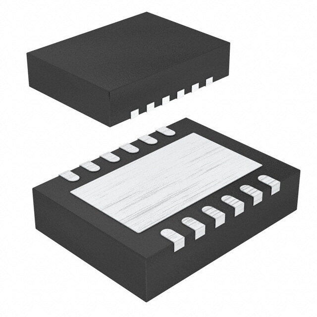
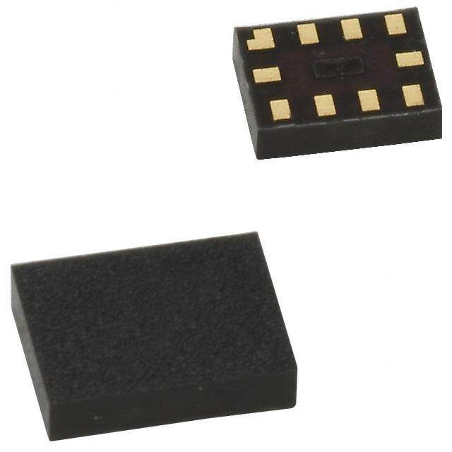
| 产品图片 |
|
| rohs | 符合RoHS无铅 / 符合限制有害物质指令(RoHS)规范要求 |
| 产品系列 | 电源管理 IC,电池管理,Texas Instruments BQ29413DCTT- |
| 数据手册 | |
| 产品型号 | BQ29413DCTT |
| 产品种类 | 电池管理 |
| 产品类型 | Battery Protection |
| 供应商器件封装 | SM8 |
| 其它名称 | 296-32041-1 |
| 功能 | 过压/欠压保护 |
| 包装 | 剪切带 (CT) |
| 单位重量 | 23.400 mg |
| 商标 | Texas Instruments |
| 安装类型 | 表面贴装 |
| 安装风格 | SMD/SMT |
| 封装 | Reel |
| 封装/外壳 | 7-LSSOP(0.11",2.80mm 宽) |
| 封装/箱体 | SSOP-8 |
| 工作温度 | -40°C ~ 110°C |
| 工作电源电压 | 4 V to 25 V |
| 工厂包装数量 | 250 |
| 最大工作温度 | + 110 C |
| 最小工作温度 | - 40 C |
| 标准包装 | 1 |
| 电压-电源 | 4 V ~ 25 V |
| 电池化学 | 锂离子 |
| 电池类型 | Li-Ion |
| 系列 | BQ29413 |
| 输出电压 | 4.5 V |


PDF Datasheet 数据手册内容提取
bq29410, bq29411, bq29412 bq29413, bq29414 bq29415, bq29419 www.ti.com SLUS669G–AUGUST2005–REVISEDAUGUST2008 VOLTAGE PROTECTION FOR 2-, 3-, OR 4-CELL Li-Ion BATTERIES nd (2 -LEVEL PROTECTION) CheckforSamples:bq29410,bq29411,bq29412,bq29413,bq29414,bq29415,bq29419 FEATURES DESCRIPTION 1 • 2-,3-,or4-CellSecondaryProtection The bq2941x is a secondary overvoltage protection IC for 2-, 3-, or 4-cell lithium-ion battery packs that • LowPowerConsumptionI <2 µA CC incorporates a high-accuracy precision overvoltage [VCELL <V ] (ALL) (PROTECT) detection circuit. It includes a programmable delay • FixedHighAccuracyOvervoltageProtection circuitforovervoltagedetectiontime. Threshold FUNCTION – bq29410=4.35V – bq29411=4.40V Each cell in a multiple-cell pack is compared to an internal reference voltage. If one cell reaches an – bq29412=4.45V overvoltage condition, the protection sequence – bq29413=4.50V begins. The bq2941x device starts charging an – bq29414=4.55V external capacitor through the CD pin. When the CD pin voltage reaches 1.2 V, the OUT pin changes from – bq29415=4.60V alowleveltoahighlevel. – bq29419=4.30V • ProgrammableDelayTimeofDetection DCT PACKAGE (TOP VIEW) • HighPowerSupplyRippleRejection • StableDuringPulseChargeOperation OUT 1 8 VC1 VDD 2 7 VC2 APPLICATIONS CD 3 6 VC3 • 2nd-LevelOvervoltageProtectioninLi-Ion VC4 4 5 GND BatteryPacksin: – NotebookComputers PW PACKAGE – PortableInstrumentation (TOP VIEW) – PortableEquipment VC1 1 8 OUT VC2 2 7 VDD VC3 3 6 CD GND 4 5 VC4 1 Pleasebeawarethatanimportantnoticeconcerningavailability,standardwarranty,anduseincriticalapplicationsof TexasInstrumentssemiconductorproductsanddisclaimerstheretoappearsattheendofthisdatasheet. PRODUCTIONDATAinformationiscurrentasofpublicationdate. Copyright©2005–2008,TexasInstrumentsIncorporated Products conform to specifications per the terms of the Texas Instruments standard warranty. Production processing does not necessarilyincludetestingofallparameters.
bq29410, bq29411, bq29412 bq29413, bq29414 bq29415, bq29419 SLUS669G –AUGUST 2005–REVISED AUGUST 2008 www.ti.com This integrated circuit can be damaged by ESD. Texas Instruments recommends that all integrated circuits be handled with appropriateprecautions.Failuretoobserveproperhandlingandinstallationprocedurescancausedamage. ESDdamagecanrangefromsubtleperformancedegradationtocompletedevicefailure.Precisionintegratedcircuitsmaybemore susceptibletodamagebecauseverysmallparametricchangescouldcausethedevicenottomeetitspublishedspecifications. ORDERINGINFORMATION(1) PACKAGE(3) T V (2) A (PROTECT) MSOP(DCT) SYMBOL SSOP(PW) bq29419DCTR 4.30V CJQ bq29419PWG4 bq29419PWRG4 bq29419DCTT bq29410DCT3R bq29410PW bq29410PWR 4.35V bq29410DCTR CJG bq29410PWG4 bq29410PWRG4 bq29410DCTT bq29411DCT3R bq29411PW bq29411PWR 4.40V bq29411DCTR CJH bq29411PWG4 bq29411PWRG4 bq29411DCTT –40°Cto110°C bq29412DCT3R bq29412PW bq29412PWR 4.45V bq29412DCTR CJJ bq29412PWG4 bq29412PWRG4 bq29412DCTT bq29413DCTR 4.50V CJk bq29413PW bq29413PWR bq29413DCTT bq29414DCTR 4.55V CJL bq29414PW bq29414PWR bq29414DCTT bq29415DCTR 4.60V CJM bq29415PW bq29415PWR bq29415DCTT (1) Forthemostcurrentpackageandorderinginformation,seethePackageOptionAddendumattheendofthisdocument,orseetheTI websiteatwww.ti.com. (2) ContactyourlocalTexasInstrumentsrepresentativeorsalesofficeforalternativeovervoltagethresholdoptions. (3) The"R"suffixindicatestape-and-reelpackaging. ABSOLUTE MAXIMUM RATINGS overoperatingfree-airtemperaturerangeunlessotherwisenoted(1) (2) UNIT Supplyvoltagerange VDD –0.3Vto28V VC1,VC2,VC3,VC4 –0.3Vto28V Inputvoltagerange VC1TOVC2,VC2TOVC3,VC3TOVC4,VC4TOGND –0.3Vto8V OUT –0.3Vto28V Outputvoltagerange CD –0.3Vto28V Continuoustotalpowerdissipation SeeDissipationRatingTable Storagetemperaturerange,T –65°Cto150°C stg Leadtemperature(soldering,10s) 300°C (1) Stressesbeyondthoselistedunder"absolutemaximumratings"maycausepermanentdamagetothedevice.Thesearestressratings only,andfunctionaloperationofthedeviceattheseoranyotherconditionsbeyondthoseindicatedunder"recommendedoperating conditions"isnotimplied.Exposuretoabsolute-maximum-ratedconditionsforextendedperiodsmayaffectdevicereliability. (2) AllvoltagesarewithrespecttogroundofthisdeviceexceptthedifferentialvoltageofVC1-VC2,VC2-VC3,VC3-VC4,andVC4-GND. PACKAGE DISSIPATION RATINGS T =25°C DERATINGFACTOR T =70°C T =85°C PACKAGE A A A POWERRATING ABOVET =25°C POWERRATING POWERRATING A DCT 412mW 3.3mW/°C 264mW 214mW PW 525mW 4.2mW/°C 336mW 273mW 2 SubmitDocumentationFeedback Copyright©2005–2008,TexasInstrumentsIncorporated ProductFolderLinks:bq29410bq29411 bq29412 bq29413 bq29414bq29415 bq29419
bq29410, bq29411, bq29412 bq29413, bq29414 bq29415, bq29419 www.ti.com SLUS669G–AUGUST2005–REVISEDAUGUST2008 RECOMMENDED OPERATING CONDITIONS MIN NOM MAX UNIT V Supplyvoltage 4 25 V DD VC1,VC2,VC3,VC4 0 25 V Inputvoltagerange V I VCn–VC(n=1),(n=1,2,3),VC4–GND 0 5 t Delaytimecapacitance 0.22 µF d(CD) R Voltage-monitorfilterresistance 100 1k Ω IN C Voltage-monitorfiltercapacitance 0.01 0.1 µF IN R Supply-voltagefilterresistance 0 1 kΩ VD C Supply-voltagefiltercapacitance 0.1 µF VD T Operatingambienttemperaturerange –40 110 °C A ELECTRICAL CHARACTERISTICS overrecommendedoperatingfree-airtemperaturerange,T =25°C(unlessotherwisenoted) A PARAMETER TESTCONDITION MIN NOM MAX UNIT T =25°C 25 35 A Overvoltagedetection V T =–20°Cto85°C 25 50 mV (OA) accuracy A T =–40°Cto110°C 80 A bq29410 4.35 bq29411 4.40 bq29412 4.45 Overvoltage V bq29413 4.50 V (PROTECT) detectionvoltage bq29414 4.55 bq29415 4.60 bq29419 4.30 Overvoltagedetection bq29410/11/12/13/14/15 320 V mV hys hysteresis bq29419 250 320 450 V2,V3,VC4input,V =VC1 I Inputcurrent DD 0.3 µA IN VC1=VC2=VC3=VC4=3.5V(seeFigure1) Overvoltagedetectiondelay t V =VC1,CD=0.22µF 1 1.5 2 S D1 time DD I CDGNDclampcurrent V =VC1,CD=1V 5 12 µA (CD_dis) DD V =VC1, DD VC1–VC2=VC2–VC3=VC3–VC4=VC4–GND=3.5V 2 3 (seeFigure1) I Supplycurrent µA CC V =VC1, DD VC1–VC2=VC2–VC3=VC3–VC4=VC4–GND=2.3V 1.5 2.5 (seeFigure1) VC1–VC2=VC2–VC3=VC3–VC4=VC4–GND= 7 V Max,V =14V,I =0mA (PROTECT) DD OH V OUTpindrivevoltage V (OUT) VC1=VC2=VC3=VC4=V Max, (PROTECT) 1.5 2 2.5 V =4.3V,T =0°Cto70°C,I =40μA DD A OH OUT=3V, I High-leveloutputcurrent VC1–VC2=VC2–VC3=VC3–VC4=VC4–GND= –1 mA OH V Max,V =14V (PROTECT) DD OUT=0.1V,V =VC1, I Low-leveloutputcurrent DD 5 µA OL VC1–VC2=VC2–VC3=VC3–VC4=VC4–GND=3.5V Copyright©2005–2008,TexasInstrumentsIncorporated SubmitDocumentationFeedback 3 ProductFolderLinks:bq29410bq29411 bq29412 bq29413 bq29414bq29415 bq29419
bq29410, bq29411, bq29412 bq29413, bq29414 bq29415, bq29419 SLUS669G –AUGUST 2005–REVISED AUGUST 2008 www.ti.com 111 OOUUTT VVCC11 888 222 VVDDDD VVCC22 887 3 CCDD VVCC33 666 4 VVCC44 GGNNDD 555 Figure1. I ,I Measurement(DCTPackage) CC IN TerminalFunctions TERMINAL MSOP TSSOP DESCRIPTION NAME (DCT) (PW) 8 1 VC1 Sensevoltageinputformostpositivecell 7 2 VC2 Sensevoltageinputforsecondmostpositivecell 6 3 VC3 Sensevoltageinputforthirdmostpositivecell 5 4 GND Groundpin 4 5 VC4 Sensevoltageinputforleastpositivecell 3 6 CD Anexternalcapacitorisconnectedtodeterminetheprogrammabledelaytime 2 7 VDD Powersupply 1 8 OUT Output 4 SubmitDocumentationFeedback Copyright©2005–2008,TexasInstrumentsIncorporated ProductFolderLinks:bq29410bq29411 bq29412 bq29413 bq29414bq29415 bq29419
bq29410, bq29411, bq29412 bq29413, bq29414 bq29415, bq29419 www.ti.com SLUS669G–AUGUST2005–REVISEDAUGUST2008 FUNCTIONALBLOCKDIAGRAM RVD CVD VDD VC1 RIN ICD= 0.2 A (TYP) CIN VC2 RIN CIN VC3 OUT RIN CIN VC4 1.2 V (TYP) RIN CIN GND CD C (DELAY) OVERVOLTAGE PROTECTION When one of the cell voltages exceeds V , an internal current source begins to charge the capacitor, (PROTECT) C , connected to the CD pin. If the voltage at the CD pin, V reaches 1.2 V, the OUT pin is activated and (DELAY) CD, transitions high. An externally connected NCH FET is activiated and blows the external fuse in the positive batteryrail;seethefunctionalblockdiagram. If all cell voltages fall below V before the voltage at pin CD reaches 1.2 V, the delay time does not run (PROTECT) out. An internal switch clamps the CD pin to GND and discharges the capacitor, C , and secures the full (DELAY) delaytimeforthenextoccurringovervoltageevent. OncethepinOUTisactivated,ittransitionsbackfromhightolowafterallbatterycellsreachV –V (PROTECT) hys. DELAY TIME CALCULATION Thedelaytimeiscalculatedasfollows: (cid:3) (cid:4) 1.2V(cid:1)C(DELAY) td(cid:2) I CD (cid:3)td(cid:1)ICD(cid:4) C(DELAY)(cid:2) 1.2V WhereI =CDcurrentsource=0.18 µA (CD) Copyright©2005–2008,TexasInstrumentsIncorporated SubmitDocumentationFeedback 5 ProductFolderLinks:bq29410bq29411 bq29412 bq29413 bq29414bq29415 bq29419
bq29410, bq29411, bq29412 bq29413, bq29414 bq29415, bq29419 SLUS669G –AUGUST 2005–REVISED AUGUST 2008 www.ti.com V(PROTECT) V(PROTECT) - Vhys Cell Voltage (VCn - VC(n-1), VC4 - GND) 1.2 V CD tDELAY OUT td = (1.2 V x CDELAY)/ICD Figure2. TimingforOvervoltageSensing APPLICATION INFORMATION BATTERY CONNECTIONS ThefollowingdiagramsshowtheDCTpackagedeviceindifferentcellconfigurations. 111 OOUUTT VVCC11 888 111 OOOUUUTTT VVVCCC111 888 222 VVDDDD VVCC22 887 222 VVVDDDDDD VVVCCC222 887 3 CCDD VVCC33 666 223 CCCDDD VVVCCC333 666 4 VVCC44 GGNNDD 555 224 VVVCCC444 GGGNNNDDD 555 Figure3.4-SeriesCellConfiguration Figure4.3-SeriesCellConfiguration (ConnecttogetherVC1andVC2) 6 SubmitDocumentationFeedback Copyright©2005–2008,TexasInstrumentsIncorporated ProductFolderLinks:bq29410bq29411 bq29412 bq29413 bq29414bq29415 bq29419
bq29410, bq29411, bq29412 bq29413, bq29414 bq29415, bq29419 www.ti.com SLUS669G–AUGUST2005–REVISEDAUGUST2008 1 OUT VC1 8 2 VDD VC2 77 36 CD VC3 6 4 VC4 GND 5 Figure5. 2-SeriesCellConfiguration CELL CONNECTIONS Topreventincorrectoutputactivation,thefollowingconnectionsequencesmustbeused. 4-SeriesCellConfiguration • VC1(=VDD)→VC2 →VC3→VC4 →GNDor • GND→VC4→VC3 →VC2→VC1(=VDD) 3-SeriesCellConfiguration • VC1(=VC2=VDD)→VC3 →VC4→GNDor • GND→VC4→VC3 →VC1(=VC2=VDD) 2-SeriesCellConfiguration • VC1(=VC2=VC3=VDD) →VC4→GNDor • GND→VC4→VC1(=VC2=VC3=VDD) Copyright©2005–2008,TexasInstrumentsIncorporated SubmitDocumentationFeedback 7 ProductFolderLinks:bq29410bq29411 bq29412 bq29413 bq29414bq29415 bq29419
PACKAGE OPTION ADDENDUM www.ti.com 6-Feb-2020 PACKAGING INFORMATION Orderable Device Status Package Type Package Pins Package Eco Plan Lead/Ball Finish MSL Peak Temp Op Temp (°C) Device Marking Samples (1) Drawing Qty (2) (6) (3) (4/5) BQ29410DCT3R ACTIVE SM8 DCT 8 3000 Pb-Free SNBI Level-1-260C-UNLIM -40 to 110 CJG (RoHS) W BQ29410DCT3RE6 ACTIVE SM8 DCT 8 3000 Pb-Free SNBI Level-1-260C-UNLIM -40 to 110 CJG (RoHS) W BQ29410DCTR ACTIVE SM8 DCT 8 3000 Green (RoHS NIPDAU Level-1-260C-UNLIM -40 to 110 CJG & no Sb/Br) W BQ29410DCTRG4 ACTIVE SM8 DCT 8 3000 Green (RoHS NIPDAU Level-1-260C-UNLIM -40 to 110 CJG & no Sb/Br) W BQ29410DCTT ACTIVE SM8 DCT 8 250 Green (RoHS NIPDAU Level-1-260C-UNLIM -40 to 110 CJG & no Sb/Br) W BQ29410PW ACTIVE TSSOP PW 8 150 Green (RoHS NIPDAU Level-1-260C-UNLIM -40 to 110 29410 & no Sb/Br) BQ29410PWR ACTIVE TSSOP PW 8 2000 Green (RoHS NIPDAU Level-1-260C-UNLIM -40 to 110 29410 & no Sb/Br) BQ29410PWRG4 ACTIVE TSSOP PW 8 2000 Green (RoHS NIPDAU Level-2-260C-1 YEAR -40 to 110 29410 & no Sb/Br) BQ29411DCT3R ACTIVE SM8 DCT 8 3000 Pb-Free SNBI Level-1-260C-UNLIM -40 to 110 CJH (RoHS) W BQ29411DCTR ACTIVE SM8 DCT 8 3000 Green (RoHS NIPDAU Level-1-260C-UNLIM -40 to 110 CJH & no Sb/Br) W BQ29411DCTRG4 ACTIVE SM8 DCT 8 3000 Green (RoHS NIPDAU Level-1-260C-UNLIM -40 to 110 CJH & no Sb/Br) W BQ29411DCTT ACTIVE SM8 DCT 8 250 Green (RoHS NIPDAU Level-1-260C-UNLIM -40 to 110 CJH & no Sb/Br) W BQ29411PW ACTIVE TSSOP PW 8 150 Green (RoHS NIPDAU Level-1-260C-UNLIM -40 to 110 29411 & no Sb/Br) BQ29411PWRG4 ACTIVE TSSOP PW 8 2000 Green (RoHS NIPDAU Level-2-260C-1 YEAR -40 to 110 29411 & no Sb/Br) BQ29412DCT3R ACTIVE SM8 DCT 8 3000 Pb-Free SNBI Level-1-260C-UNLIM -40 to 110 CJJ (RoHS) W BQ29412DCTR ACTIVE SM8 DCT 8 3000 Green (RoHS NIPDAU Level-1-260C-UNLIM -40 to 110 CJJ & no Sb/Br) W BQ29412DCTRG4 ACTIVE SM8 DCT 8 3000 Green (RoHS NIPDAU Level-1-260C-UNLIM -40 to 110 CJJ & no Sb/Br) W Addendum-Page 1
PACKAGE OPTION ADDENDUM www.ti.com 6-Feb-2020 Orderable Device Status Package Type Package Pins Package Eco Plan Lead/Ball Finish MSL Peak Temp Op Temp (°C) Device Marking Samples (1) Drawing Qty (2) (6) (3) (4/5) BQ29412DCTT ACTIVE SM8 DCT 8 250 Green (RoHS NIPDAU Level-1-260C-UNLIM -40 to 110 CJJ & no Sb/Br) W BQ29412PWR ACTIVE TSSOP PW 8 2000 Green (RoHS NIPDAU Level-1-260C-UNLIM 29412 & no Sb/Br) BQ29412PWRG4 ACTIVE TSSOP PW 8 2000 Green (RoHS NIPDAU Level-2-260C-1 YEAR 29412 & no Sb/Br) BQ29413DCTR ACTIVE SM8 DCT 8 3000 Green (RoHS NIPDAU Level-1-260C-UNLIM -40 to 110 CJK & no Sb/Br) W BQ29413DCTRG4 ACTIVE SM8 DCT 8 3000 Green (RoHS NIPDAU Level-1-260C-UNLIM -40 to 110 CJK & no Sb/Br) W BQ29413PWR ACTIVE TSSOP PW 8 2000 Green (RoHS NIPDAU Level-2-260C-1 YEAR -40 to 110 29413 & no Sb/Br) BQ29415PWR ACTIVE TSSOP PW 8 2000 Green (RoHS NIPDAU Level-2-260C-1 YEAR -40 to 110 2915 & no Sb/Br) BQ29419PW ACTIVE TSSOP PW 8 150 Green (RoHS NIPDAU Level-2-260C-1 YEAR -40 to 110 29419 & no Sb/Br) BQ29419PWG4 ACTIVE TSSOP PW 8 150 Green (RoHS NIPDAU Level-2-260C-1 YEAR -40 to 110 29419 & no Sb/Br) BQ29419PWR ACTIVE TSSOP PW 8 2000 Green (RoHS NIPDAU Level-2-260C-1 YEAR -40 to 110 29419 & no Sb/Br) (1) The marketing status values are defined as follows: ACTIVE: Product device recommended for new designs. LIFEBUY: TI has announced that the device will be discontinued, and a lifetime-buy period is in effect. NRND: Not recommended for new designs. Device is in production to support existing customers, but TI does not recommend using this part in a new design. PREVIEW: Device has been announced but is not in production. Samples may or may not be available. OBSOLETE: TI has discontinued the production of the device. (2) RoHS: TI defines "RoHS" to mean semiconductor products that are compliant with the current EU RoHS requirements for all 10 RoHS substances, including the requirement that RoHS substance do not exceed 0.1% by weight in homogeneous materials. Where designed to be soldered at high temperatures, "RoHS" products are suitable for use in specified lead-free processes. TI may reference these types of products as "Pb-Free". RoHS Exempt: TI defines "RoHS Exempt" to mean products that contain lead but are compliant with EU RoHS pursuant to a specific EU RoHS exemption. Green: TI defines "Green" to mean the content of Chlorine (Cl) and Bromine (Br) based flame retardants meet JS709B low halogen requirements of <=1000ppm threshold. Antimony trioxide based flame retardants must also meet the <=1000ppm threshold requirement. (3) MSL, Peak Temp. - The Moisture Sensitivity Level rating according to the JEDEC industry standard classifications, and peak solder temperature. Addendum-Page 2
PACKAGE OPTION ADDENDUM www.ti.com 6-Feb-2020 (4) There may be additional marking, which relates to the logo, the lot trace code information, or the environmental category on the device. (5) Multiple Device Markings will be inside parentheses. Only one Device Marking contained in parentheses and separated by a "~" will appear on a device. If a line is indented then it is a continuation of the previous line and the two combined represent the entire Device Marking for that device. (6) Lead/Ball Finish - Orderable Devices may have multiple material finish options. Finish options are separated by a vertical ruled line. Lead/Ball Finish values may wrap to two lines if the finish value exceeds the maximum column width. Important Information and Disclaimer:The information provided on this page represents TI's knowledge and belief as of the date that it is provided. TI bases its knowledge and belief on information provided by third parties, and makes no representation or warranty as to the accuracy of such information. Efforts are underway to better integrate information from third parties. TI has taken and continues to take reasonable steps to provide representative and accurate information but may not have conducted destructive testing or chemical analysis on incoming materials and chemicals. TI and TI suppliers consider certain information to be proprietary, and thus CAS numbers and other limited information may not be available for release. In no event shall TI's liability arising out of such information exceed the total purchase price of the TI part(s) at issue in this document sold by TI to Customer on an annual basis. Addendum-Page 3
PACKAGE MATERIALS INFORMATION www.ti.com 21-Sep-2019 TAPE AND REEL INFORMATION *Alldimensionsarenominal Device Package Package Pins SPQ Reel Reel A0 B0 K0 P1 W Pin1 Type Drawing Diameter Width (mm) (mm) (mm) (mm) (mm) Quadrant (mm) W1(mm) BQ29410DCT3R SM8 DCT 8 3000 180.0 13.0 3.35 4.5 1.55 4.0 12.0 Q3 BQ29410DCTR SM8 DCT 8 3000 180.0 13.0 3.35 4.5 1.55 4.0 12.0 Q3 BQ29410DCTT SM8 DCT 8 250 180.0 13.0 3.35 4.5 1.55 4.0 12.0 Q3 BQ29410PWR TSSOP PW 8 2000 330.0 12.4 7.0 3.6 1.6 8.0 12.0 Q1 BQ29410PWRG4 TSSOP PW 8 2000 330.0 12.4 7.0 3.6 1.6 8.0 12.0 Q1 BQ29411DCT3R SM8 DCT 8 3000 180.0 13.0 3.35 4.5 1.55 4.0 12.0 Q3 BQ29411DCTR SM8 DCT 8 3000 180.0 13.0 3.35 4.5 1.55 4.0 12.0 Q3 BQ29411DCTT SM8 DCT 8 250 180.0 13.0 3.35 4.5 1.55 4.0 12.0 Q3 BQ29411PWRG4 TSSOP PW 8 2000 330.0 12.4 7.0 3.6 1.6 8.0 12.0 Q1 BQ29412DCTR SM8 DCT 8 3000 180.0 13.0 3.35 4.5 1.55 4.0 12.0 Q3 BQ29412DCTT SM8 DCT 8 250 180.0 13.0 3.35 4.5 1.55 4.0 12.0 Q3 BQ29412PWR TSSOP PW 8 2000 330.0 12.4 7.0 3.6 1.6 8.0 12.0 Q1 BQ29412PWRG4 TSSOP PW 8 2000 330.0 12.4 7.0 3.6 1.6 8.0 12.0 Q1 BQ29413DCTR SM8 DCT 8 3000 180.0 13.0 3.35 4.5 1.55 4.0 12.0 Q3 BQ29413PWR TSSOP PW 8 2000 330.0 12.4 7.0 3.6 1.6 8.0 12.0 Q1 BQ29415PWR TSSOP PW 8 2000 330.0 12.4 7.0 3.6 1.6 8.0 12.0 Q1 BQ29419PWR TSSOP PW 8 2000 330.0 12.4 7.0 3.6 1.6 8.0 12.0 Q1 PackMaterials-Page1
PACKAGE MATERIALS INFORMATION www.ti.com 21-Sep-2019 *Alldimensionsarenominal Device PackageType PackageDrawing Pins SPQ Length(mm) Width(mm) Height(mm) BQ29410DCT3R SM8 DCT 8 3000 182.0 182.0 20.0 BQ29410DCTR SM8 DCT 8 3000 182.0 182.0 20.0 BQ29410DCTT SM8 DCT 8 250 182.0 182.0 20.0 BQ29410PWR TSSOP PW 8 2000 367.0 367.0 35.0 BQ29410PWRG4 TSSOP PW 8 2000 367.0 367.0 35.0 BQ29411DCT3R SM8 DCT 8 3000 182.0 182.0 20.0 BQ29411DCTR SM8 DCT 8 3000 182.0 182.0 20.0 BQ29411DCTT SM8 DCT 8 250 182.0 182.0 20.0 BQ29411PWRG4 TSSOP PW 8 2000 367.0 367.0 35.0 BQ29412DCTR SM8 DCT 8 3000 182.0 182.0 20.0 BQ29412DCTT SM8 DCT 8 250 182.0 182.0 20.0 BQ29412PWR TSSOP PW 8 2000 367.0 367.0 35.0 BQ29412PWRG4 TSSOP PW 8 2000 367.0 367.0 35.0 BQ29413DCTR SM8 DCT 8 3000 182.0 182.0 20.0 BQ29413PWR TSSOP PW 8 2000 367.0 367.0 35.0 BQ29415PWR TSSOP PW 8 2000 367.0 367.0 35.0 BQ29419PWR TSSOP PW 8 2000 367.0 367.0 35.0 PackMaterials-Page2
PACKAGE OUTLINE DCT0008A SSOP - 1.3 mm max height SCALE 3.500 SMALL OUTLINE PACKAGE C 4.25 TYP 3.75 SEATING PLANE A PIN 1 ID AREA 0.1 C 6X 0.65 8 1 3.15 2X 2.75 1.95 NOTE 3 4 5 0.30 8X 0.15 2.9 0.13 C A B 1.3 B 2.7 1.0 NOTE 4 SEE DETAIL A (0.15) TYP 0.25 GAGE PLANE 0.1 0.6 0 - 8 0.0 0.2 DETAIL A TYPICAL 4220784/B 07/2020 NOTES: 1. All linear dimensions are in millimeters. Dimensions in parenthesis are for reference only. Dimensioning and tolerancing per ASME Y14.5M. 2. This drawing is subject to change without notice. 3. This dimension does not include mold flash, protrusions, or gate burrs. Mold flash, protrusions, or gate burrs shall not exceed 0.15 mm per side. 4. This dimension does not include interlead flash. Interlead flash shall not exceed 0.25 mm per side. 5. Reference JEDEC registration MS-187. www.ti.com
EXAMPLE BOARD LAYOUT DCT0008A SSOP - 1.3 mm max height SMALL OUTLINE PACKAGE 8X (1.1) SYMM (R0.05) 1 TYP 8 8X (0.4) SYMM 6X (0.65) 5 4 (3.8) LAND PATTERN EXAMPLE EXPOSED METAL SHOWN SCALE:15X SOOPLEDNEINRG MASK METAL MSOELTDAEL RU NMDAESRK SOOPLEDNEINRG MASK EXPOSED METAL EXPOSED METAL 0.07 MAX 0.07 MIN ALL AROUND ALL AROUND NON SOLDER MASK SOLDER MASK DEFINED DEFINED SOLDER MASK DETAILS 4220784/B 07/2020 NOTES: (continued) 6. Publication IPC-7351 may have alternate designs. 7. Solder mask tolerances between and around signal pads can vary based on board fabrication site. www.ti.com
EXAMPLE STENCIL DESIGN DCT0008A SSOP - 1.3 mm max height SMALL OUTLINE PACKAGE 8X (1.1) SYMM 1 8 8X (0.4) SYMM 6X (0.65) 5 4 (3.8) SOLDER PASTE EXAMPLE BASED ON 0.125 mm THICK STENCIL SCALE:15X 4220784/B 07/2020 NOTES: (continued) 8. Laser cutting apertures with trapezoidal walls and rounded corners may offer better paste release. IPC-7525 may have alternate design recommendations. 9. Board assembly site may have different recommendations for stencil design. www.ti.com
PACKAGE OUTLINE PW0008A TSSOP - 1.2 mm max height SCALE 2.800 SMALL OUTLINE PACKAGE C 6.6 TYP SEATING PLANE 6.2 PIN 1 ID A 0.1 C AREA 6X 0.65 8 1 3.1 2X 2.9 NOTE 3 1.95 4 5 0.30 8X 0.19 4.5 1.2 MAX B 0.1 C A B 4.3 NOTE 4 (0.15) TYP SEE DETAIL A 0.25 GAGE PLANE 0.15 0.75 0 - 8 0.05 0.50 DETAIL A TYPICAL 4221848/A 02/2015 NOTES: 1. All linear dimensions are in millimeters. Any dimensions in parenthesis are for reference only. Dimensioning and tolerancing per ASME Y14.5M. 2. This drawing is subject to change without notice. 3. This dimension does not include mold flash, protrusions, or gate burrs. Mold flash, protrusions, or gate burrs shall not exceed 0.15 mm per side. 4. This dimension does not include interlead flash. Interlead flash shall not exceed 0.25 mm per side. 5. Reference JEDEC registration MO-153, variation AA. www.ti.com
EXAMPLE BOARD LAYOUT PW0008A TSSOP - 1.2 mm max height SMALL OUTLINE PACKAGE 8X (1.5) 8X (0.45) SYMM (R0.05) 1 TYP 8 SYMM 6X (0.65) 5 4 (5.8) LAND PATTERN EXAMPLE SCALE:10X SOOPLEDNEINRG MASK METAL MSOELTDAEL RU NMDAESRK SOOPLEDNEINRG MASK 0.05 MAX 0.05 MIN ALL AROUND ALL AROUND NON SOLDER MASK SOLDER MASK DEFINED DEFINED SOLDER MASK DETAILS NOT TO SCALE 4221848/A 02/2015 NOTES: (continued) 6. Publication IPC-7351 may have alternate designs. 7. Solder mask tolerances between and around signal pads can vary based on board fabrication site. www.ti.com
EXAMPLE STENCIL DESIGN PW0008A TSSOP - 1.2 mm max height SMALL OUTLINE PACKAGE 8X (1.5) SYMM (R0.05) TYP 8X (0.45) 1 8 SYMM 6X (0.65) 5 4 (5.8) SOLDER PASTE EXAMPLE BASED ON 0.125 mm THICK STENCIL SCALE:10X 4221848/A 02/2015 NOTES: (continued) 8. Laser cutting apertures with trapezoidal walls and rounded corners may offer better paste release. IPC-7525 may have alternate design recommendations. 9. Board assembly site may have different recommendations for stencil design. www.ti.com
IMPORTANTNOTICEANDDISCLAIMER TI PROVIDES TECHNICAL AND RELIABILITY DATA (INCLUDING DATASHEETS), DESIGN RESOURCES (INCLUDING REFERENCE DESIGNS), APPLICATION OR OTHER DESIGN ADVICE, WEB TOOLS, SAFETY INFORMATION, AND OTHER RESOURCES “AS IS” AND WITH ALL FAULTS, AND DISCLAIMS ALL WARRANTIES, EXPRESS AND IMPLIED, INCLUDING WITHOUT LIMITATION ANY IMPLIED WARRANTIES OF MERCHANTABILITY, FITNESS FOR A PARTICULAR PURPOSE OR NON-INFRINGEMENT OF THIRD PARTY INTELLECTUAL PROPERTY RIGHTS. These resources are intended for skilled developers designing with TI products. You are solely responsible for (1) selecting the appropriate TI products for your application, (2) designing, validating and testing your application, and (3) ensuring your application meets applicable standards, and any other safety, security, or other requirements. These resources are subject to change without notice. TI grants you permission to use these resources only for development of an application that uses the TI products described in the resource. Other reproduction and display of these resources is prohibited. No license is granted to any other TI intellectual property right or to any third party intellectual property right. TI disclaims responsibility for, and you will fully indemnify TI and its representatives against, any claims, damages, costs, losses, and liabilities arising out of your use of these resources. TI’s products are provided subject to TI’s Terms of Sale (www.ti.com/legal/termsofsale.html) or other applicable terms available either on ti.com or provided in conjunction with such TI products. TI’s provision of these resources does not expand or otherwise alter TI’s applicable warranties or warranty disclaimers for TI products. Mailing Address: Texas Instruments, Post Office Box 655303, Dallas, Texas 75265 Copyright © 2020, Texas Instruments Incorporated