ICGOO在线商城 > 集成电路(IC) > PMIC - 电源管理 - 专用 > BQ24640RVAR
- 型号: BQ24640RVAR
- 制造商: Texas Instruments
- 库位|库存: xxxx|xxxx
- 要求:
| 数量阶梯 | 香港交货 | 国内含税 |
| +xxxx | $xxxx | ¥xxxx |
查看当月历史价格
查看今年历史价格
BQ24640RVAR产品简介:
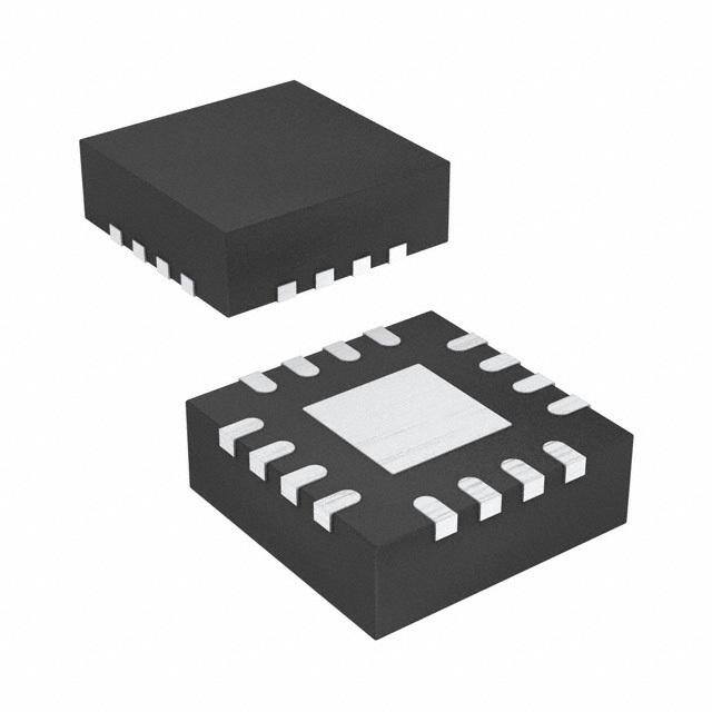
ICGOO电子元器件商城为您提供BQ24640RVAR由Texas Instruments设计生产,在icgoo商城现货销售,并且可以通过原厂、代理商等渠道进行代购。 BQ24640RVAR价格参考。Texas InstrumentsBQ24640RVAR封装/规格:PMIC - 电源管理 - 专用, Supercapacitor Charger PMIC 16-VQFN (3.5x3.5)。您可以下载BQ24640RVAR参考资料、Datasheet数据手册功能说明书,资料中有BQ24640RVAR 详细功能的应用电路图电压和使用方法及教程。
| 参数 | 数值 |
| 产品目录 | 集成电路 (IC) |
| 描述 | IC SYNC SW-MODE BAT CHRGR 16VQFN |
| 产品分类 | |
| 品牌 | Texas Instruments |
| 数据手册 | |
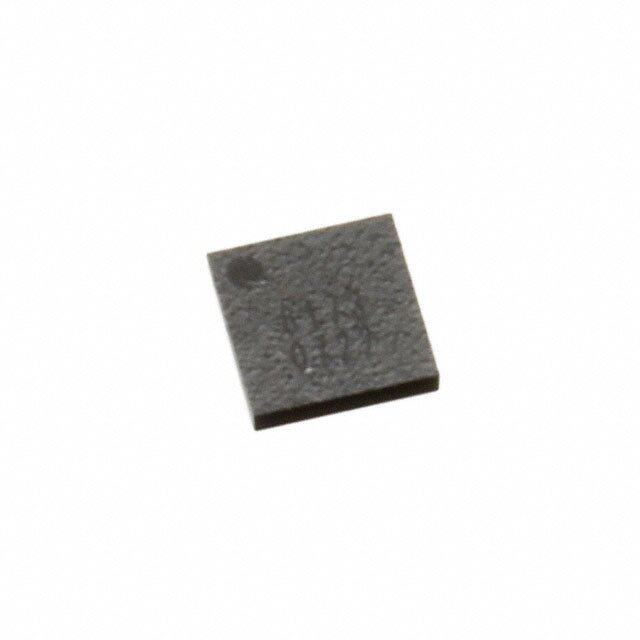
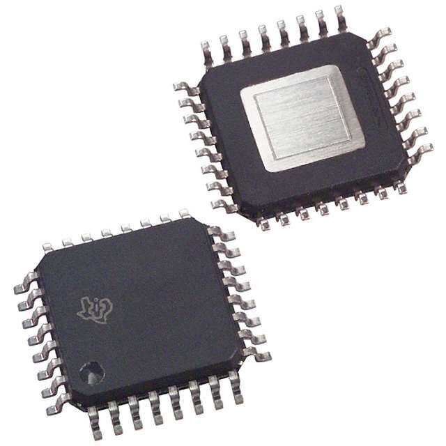
| 产品图片 |
|
| 产品型号 | BQ24640RVAR |
| PCN设计/规格 | |
| rohs | 无铅 / 符合限制有害物质指令(RoHS)规范要求 |
| 产品系列 | - |
| 供应商器件封装 | 16-VQFN 裸露焊盘(3.5x3.5) |
| 其它名称 | 296-27258-1 |
| 包装 | 剪切带 (CT) |
| 安装类型 | 表面贴装 |
| 封装/外壳 | 16-VFQFN 裸露焊盘 |
| 工作温度 | -40°C ~ 85°C |
| 应用 | 超级电容器充电器 |
| 标准包装 | 1 |
| 电压-电源 | 5 V ~ 28 V |
| 电流-电源 | 1mA |


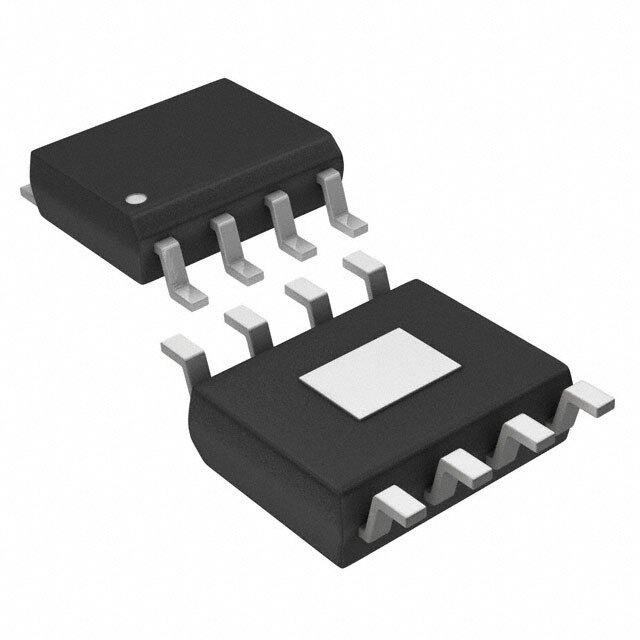


- 商务部:美国ITC正式对集成电路等产品启动337调查
- 曝三星4nm工艺存在良率问题 高通将骁龙8 Gen1或转产台积电
- 太阳诱电将投资9.5亿元在常州建新厂生产MLCC 预计2023年完工
- 英特尔发布欧洲新工厂建设计划 深化IDM 2.0 战略
- 台积电先进制程称霸业界 有大客户加持明年业绩稳了
- 达到5530亿美元!SIA预计今年全球半导体销售额将创下新高
- 英特尔拟将自动驾驶子公司Mobileye上市 估值或超500亿美元
- 三星加码芯片和SET,合并消费电子和移动部门,撤换高东真等 CEO
- 三星电子宣布重大人事变动 还合并消费电子和移动部门
- 海关总署:前11个月进口集成电路产品价值2.52万亿元 增长14.8%



PDF Datasheet 数据手册内容提取
Product Sample & Technical Tools & Support & Reference Folder Buy Documents Software Community Design bq24640 SLUSA44A–MARCH2010–REVISEDJULY2015 bq24640 High-Efficiency Synchronous Switched-Mode Super Capacitor Charger 1 Features 2 Applications • ChargeSuperCapacitorPackFrom2.1Vto26V • MemoryBackupSystems 1 • CC/CVChargeProfileFrom0VWithout • IndustrialUPSSystemsandPowerTransient Precharge Buffering • 600-kHzNMOS-NMOSSynchronousBuck • BridgePowertoBuffertheBattery Controller 3 Description • Over90%Efficiencyforupto10-ACharge Current The bq24640 device is a highly integrated switched- mode super capacitor charge controller. The device • 5-Vto28-VVCCInputVoltageRange offers a constant-frequency synchronous PWM • Accuracy controller with high accuracy charge current, voltage – ±0.5%ChargeVoltageRegulation regulation,andchargestatusmonitoring. – ±3%ChargeCurrentRegulation The bq24640 charges a super capacitor in two • HighIntegration phases: constant current and constant voltage (CC/CV). The device can charge super capacitors – InternalLoopCompensation from 0 V with current set on the ISET pin. When the – InternalDigitalSoftStart super capacitor voltage reaches the programmed • Safety targetvoltage,chargecurrentbeginstaperingdown. – InputOvervoltageProtection The bq24640 enters a low-current sleep mode – CapacitorTemperatureSensingHotandCold (<15 μA) when the input voltage falls below the ChargeSuspend outputcapacitorvoltage. – ThermalShutdown The bq24640 has an input CE pin to enable and • StatusOutputs disable charge, and the STAT and PG output pins report charge and adapter status. The TS pin on the – AdapterPresent bq24640 monitors the temperature of the capacitor – ChargerOperationStatus andsuspendschargeduringhotandcoldconditions. • ChargeEnablePin DeviceInformation(1) • 30-nsDriverDeadTimeand99.5%Maximum EffectiveDutyCycle PARTNUMBER PACKAGE BODYSIZE(NOM) • AutomaticSleepModeforLowPower bq24640 VQFN(16) 3.50mm×3.50mm Consumption (1) For all available packages, see the orderable addendum at theendofthedatasheet. – <15-µAOff-StateSuperCapacitorDischarge Current – <1.5-mAOff-StateInputQuiescentCurrent SimplifiedSchematic ADAPTER CE VREF HIDRV ISET PH STAT bq24640 LODRV SuCpaepr ADAPTER PG SRP VREF SRN VFB TS 1 An IMPORTANT NOTICE at the end of this data sheet addresses availability, warranty, changes, use in safety-critical applications, intellectualpropertymattersandotherimportantdisclaimers.PRODUCTIONDATA.
bq24640 SLUSA44A–MARCH2010–REVISEDJULY2015 www.ti.com Table of Contents 1 Features.................................................................. 1 7.4 DeviceFunctionalModes........................................16 2 Applications........................................................... 1 8 ApplicationandImplementation........................ 17 3 Description............................................................. 1 8.1 ApplicationInformation............................................17 4 RevisionHistory..................................................... 2 8.2 TypicalApplication..................................................17 5 PinConfigurationandFunctions......................... 3 9 PowerSupplyRecommendations...................... 21 6 Specifications......................................................... 4 10 Layout................................................................... 21 6.1 AbsoluteMaximumRatings .....................................4 10.1 LayoutGuidelines.................................................21 6.2 ESDRatings..............................................................4 10.2 LayoutExamples...................................................22 6.3 RecommendedOperatingConditions.......................5 11 DeviceandDocumentationSupport................. 23 6.4 ThermalInformation..................................................5 11.1 DeviceSupport......................................................23 6.5 ElectricalCharacteristics...........................................5 11.2 DocumentationSupport........................................23 6.6 TypicalCharacteristics..............................................8 11.3 CommunityResources..........................................23 7 DetailedDescription............................................ 10 11.4 Trademarks...........................................................23 7.1 Overview.................................................................10 11.5 ElectrostaticDischargeCaution............................23 7.2 FunctionalBlockDiagram.......................................11 11.6 Glossary................................................................23 7.3 FeatureDescription.................................................12 12 Mechanical,Packaging,andOrderable Information........................................................... 23 4 Revision History NOTE:Pagenumbersforpreviousrevisionsmaydifferfrompagenumbersinthecurrentversion. ChangesfromOriginal(March2010)toRevisionA Page • AddedESDRatingstable,FeatureDescriptionsection,DeviceFunctionalModes,ApplicationandImplementation section,PowerSupplyRecommendationssection,Layoutsection,DeviceandDocumentationSupportsection,and Mechanical,Packaging,andOrderableInformationsection.................................................................................................. 1 2 SubmitDocumentationFeedback Copyright©2010–2015,TexasInstrumentsIncorporated ProductFolderLinks:bq24640
bq24640 www.ti.com SLUSA44A–MARCH2010–REVISEDJULY2015 5 Pin Configuration and Functions RVAPackage 16-PinVQFNWithExposedThermalPad TopView V T RV R BTS HID PH LOD 16 15 14 13 VCC 1 12 REGN CE 2 11 GND STAT 3 10 SRP TS 4 9 SRN 5 6 7 8 G F T B P E E F R S V V I PinFunctions PIN TYPE(1) DESCRIPTION NAME NO. BTST 16 P PWMhigh-sidedriverpositivesupply.Connectthe0.1-μFbootstrapcapacitorfromPHtoBTST. Chargeenable,activeHIGHlogicinput.HIenablescharge,andLOdisablescharge.Connecttopulluprail CE 2 I with10-kΩresistor.Ithasaninternal1-MΩpulldownresistor. GND 11 P Low-currentsensitiveanalog/digitalground.OnPCBlayout,connectwiththermalpadunderneaththeIC. PWMhigh-sidedriveroutput.Connecttothegateofthehigh-sideN-channelpowerMOSFETwithashort HIDRV 15 O trace. Chargecurrentsetpoint.ThevoltageissetthroughavoltagedividerfromVREFtoISETandtoGND. V ISET 7 I I = ISET CHG 20 ´ R SR PWMlow-sidedriveroutput.Connecttothegateofthelow-sideN-channelpowerMOSFETwithashort LODRV 13 O trace. Open-drainactive-lowadapterstatusoutput.ConnecttopulluprailthroughLEDand10-kΩresistor.TheLED PG 5 O turnsonwhenavalidisdetected,andoffinthesleepmode. Switchingnode,chargecurrentoutputinductorconnection.Connectthe0.1-μFbootstrapcapacitorfromPH PH 14 P toBTST. PWMlow-sidedriverpositive6-Vsupplyoutput.Connecta1-μFceramiccapacitorfromREGNtoGNDpin REGN 12 P closetotheIC.Useforlow-sidedriverandhigh-sidedriverbootstrapvoltagebysmallsignalSchottkydiode fromREGNtoBTST. Chargecurrent-senseresistor,negativeinput.A0.1-μFceramiccapacitorisplacedfromSRNtoSRPto SRN 9 I providedifferential-modefiltering.Anoptional0.1-μFceramiccapacitorisplacedfromSRNpintoGNDfor common-modefiltering. Chargecurrentsenseresistor,positiveinput.A0.1-μFceramiccapacitorisplacedfromSRNtoSRPto SRP 10 P/I providedifferential-modefiltering.A0.1-μFceramiccapacitorisplacedfromSRPpintoGNDforcommon- modefiltering. Open-drainchargestatusoutputtoindicatevariouschargeroperation.Connecttothepulluprailthroughthe STAT 3 O LEDand10-kΩ(seeTable4). Temperaturequalificationvoltageinputfornegativetemperaturecoefficientthermistor.Programthehotand TS 4 I coldtemperaturewindowwitharesistor-dividerfromVREFtoTStoGND.RecommendSEMITEC103AT-2 10-kΩthermister. (1) P-Power,I-Input,O-Output Copyright©2010–2015,TexasInstrumentsIncorporated SubmitDocumentationFeedback 3 ProductFolderLinks:bq24640
bq24640 SLUSA44A–MARCH2010–REVISEDJULY2015 www.ti.com PinFunctions(continued) PIN TYPE(1) DESCRIPTION NAME NO. ICpowerpositivesupply.Connectthrougha10-Ωresistortothecathodeofinputdiode.Placea1-μFceramic VCC 1 P capacitorfromVCCtoGNDandplaceitascloseaspossibletoICtofilteroutthenoise. Chargevoltageanalogfeedbackadjustment.ConnectaresistordividerfromoutputtoVFBtoGNDtoadjust VFB 8 I theoutputvoltage.Theinternalregulationlimitis2.1V. 3.3-Vreferencevoltageoutput.Placea1-μFceramiccapacitorfromVREFtoGNDpinclosetotheIC.This VREF 6 P voltagecouldbeusedforprogrammingchargecurrentregulationonISETandforthermalthresholdonTS.It canbeusedasthepulluprailofSTAT,andPG. ExposedpadbeneaththeIC.Alwayssolderthermalpadtotheboard,andhaveviasonthethermalpad Thermalpad — planestar-connectingtoGNDandgroundplaneforhigh-currentpowerconverter.Italsoservesasathermal padtodissipatetheheat. 6 Specifications 6.1 Absolute Maximum Ratings overoperatingfree-airtemperaturerange(unlessotherwisenoted)(1) MIN MAX UNIT VCC,SRP,SRN,STAT,PG,CE –0.3 33 PH –2 33 VFB(3) –0.3 16 Voltage (2) V REGN,LODRV,TS –0.3 7 BTST,HIDRVwithrespecttoGND –0.3 39 VREF,ISET –0.3 3.6 Maximum SRP–SRN –0.5 0.5 V differencevoltage Junction,T –40 155 J Temperature °C Storage,T –55 155 stg (1) StressesbeyondthoselistedunderAbsoluteMaximumRatingsmaycausepermanentdamagetothedevice.Thesearestressratings only,andfunctionaloperationofthedeviceattheseoranyotherconditionsbeyondthoseindicatedunderRecommendedOperating Conditionsisnotimplied.Exposuretoabsolute-maximum-ratedconditionsforextendedperiodsmayaffectdevicereliability (2) AllvoltagesarewithrespecttoGNDifnotspecified.Currentsarepositiveinto,negativeoutofthespecifiedterminal.Consultthe PackageOptionAddendumattheendofthedatasheetforthermallimitationsandconsiderations. (3) MusthaveaseriesresistorbetweenoutputtoVFBifoutputvoltageisexpectedtobegreaterthan16V.Usuallytheresistor-dividertop resistorwilltakecareofthis. 6.2 ESD Ratings VALUE UNIT Humanbodymodel(HBM),perANSI/ESDA/JEDECJS-001(1) ±2000 V(ESD) Electrostaticdischarge Chargeddevicemodel(CDM),perJEDECspecificationJESD22- ±500 V C101(2) (1) JEDECdocumentJEP155statesthat500-VHBMallowssafemanufacturingwithastandardESDcontrolprocess. (2) JEDECdocumentJEP157statesthat250-VCDMallowssafemanufacturingwithastandardESDcontrolprocess. 4 SubmitDocumentationFeedback Copyright©2010–2015,TexasInstrumentsIncorporated ProductFolderLinks:bq24640
bq24640 www.ti.com SLUSA44A–MARCH2010–REVISEDJULY2015 6.3 Recommended Operating Conditions overoperatingfree-airtemperaturerange(unlessotherwisenoted) MIN MAX UNIT VCC,SRP,SRN,STAT,PG,CE –0.3 28 PH –2 30 VFB –0.3 14 Voltage REGN,LODRV,TS –0.3 6.5 V (withrespecttoGND) BTST,HIDRVwithrespecttoGND –0.3 34 ISET –0.3 3.3 VREF 3.3 Maximumdifferencevoltage SRP–SRN –0.2 0.2 V Junctiontemperature,T 0 125 °C J 6.4 Thermal Information bq24640 THERMALMETRIC(1) RVA(VQFN) UNIT 16PINS R Junction-to-ambientthermalresistance 43.8 °C/W θJA R Junction-to-case(top)thermalresistance 81 °C/W θJC(top) R Junction-to-boardthermalresistance 16 °C/W θJB ψ Junction-to-topcharacterizationparameter 0.6 °C/W JT ψ Junction-to-boardcharacterizationparameter 15.77 °C/W JB R Junction-to-case(bottom)thermalresistance 4 °C/W θJC(bot) (1) Formoreinformationabouttraditionalandnewthermalmetrics,seetheSemiconductorandICPackageThermalMetricsapplication report,SPRA953. 6.5 Electrical Characteristics 5V≤V(VCC)≤28V,0°C<T<125°C,typicalvaluesareatT =25°C,withrespecttoGND(unlessotherwisenoted) A PARAMETER TESTCONDITIONS MIN TYP MAX UNIT OPERATINGCONDITIONS V VCCinputvoltageoperatingrange 5 28 V VCC_OP QUIESCENTCURRENTS Totaloutputdischargecurrent(sum I ofcurrentsintoVCC,BTST,PH, V <V <V (sleepmode) 15 µA OUT UVLO VCC SRN SRP,SRN,VFB),VFB≤2.1V V >V ,V >V , VCC SRN VCC UVLO 1 1.5 CE=LOW V >V ,V >V , VCC SRN VCC VCCLOWV 2 5 I AdaptersupplycurrentintoVCCpin CE=HIGH,chargedone mA AC V >V ,V >V , VCC SRN VCC VCCLOWV CE=HIGH,Charging,Qg_total=20nC, 25 V =20V VCC CHARGEVOLTAGEREGULATION V Feedbackregulationvoltage 2.1 V FB T =0°Cto85°C –0.5% 0.5% J Chargevoltageregulationaccuracy T =–40°Cto125°C –0.7% 0.7% J I LeakagecurrentintoVFBpin VFB=2.1V 100 nA VFB Copyright©2010–2015,TexasInstrumentsIncorporated SubmitDocumentationFeedback 5 ProductFolderLinks:bq24640
bq24640 SLUSA44A–MARCH2010–REVISEDJULY2015 www.ti.com Electrical Characteristics (continued) 5V≤V(VCC)≤28V,0°C<T<125°C,typicalvaluesareatT =25°C,withrespecttoGND(unlessotherwisenoted) A PARAMETER TESTCONDITIONS MIN TYP MAX UNIT CURRENTREGULATION V ISETvoltagerange 2 V ISET1 SRP-SRNcurrentsensevoltage V V =V –V 100 mV IREG_CHG range IREG_CHG SRP SRN Chargecurrentsetfactor(ampsof K RSENSE=10mΩ 5 A/V ISET1 chargecurrentpervoltonISETpin) V =40mV –3% 3% IREG_CHG V =20mV –5% 5% IREG_CHG Chargecurrentregulationaccuracy V =5mV –25% 25% IREG_CHG V =1.5mV –50% 50% IREG_CHG I LeakagecurrentintoISETpin V =2V 100 nA ISET ISET1 INPUTUNDERVOLTAGELOCKOUTCOMPARATOR(UVLO) V ACundervoltagerisingthreshold MeasureonVCC 3.65 3.85 4 V UVLO V ACundervoltagehysteresis,falling 350 mV UVLO_HYS VCCLOWVCOMPARATOR V Fallingthreshold,disablecharge MeasureonVCC 4.1 V LOWV_FALL V Risingthreshold,resumecharge 4.35 4.5 V LOWV_RISE SLEEPCOMPARATOR(REVERSEDISCHARGINGPROTECTION) V Sleepfallingthreshold V –V toentersleepmdoe 40 100 150 mV SLEEP_FALL VCC SRN Sleephysteresis 500 mV Sleeprisingdelay VCCfallingbelowSRN,DelaytopullupPG 1 µs VCCrisingaboveSRN,Delaytopulldown Sleepfallingdelay 30 ms PG V SLEEP_HYS VCCfallingbelowSRN,Delaytoentersleep Sleeprisingshutdowndeglitch 100 ms mode VCCrisingaboveSRN,Delaytoexitsleep Sleepfallingpowerupdeglitch 30 ms mode OUTOVERVOLTAGECOMPARATOR V Overvoltagerisingthreshold AspercentageofV 104% OV_RISE VFB V Overvoltagefallingthreshold AspercentageofV 102% OV_FALL VFB INPUTOVERVOLTAGECOMPARATOR(ACOV) V ACovervoltagerisingthreshold MeasuredonVCC 31 32 33 V ACOV V ACovervoltagefallinghysteresis 1 V ACOV_HYS ACovervoltagerisingdeglitch Delaytodisablecharge 1 ms ACovervoltagefallingdeglitch Delaytoresumecharge 1 ms THERMALSHUTDOWNCOMPARATOR Thermalshutdownrising T TemperatureIncreasing 145 °C SHUT temperature T Thermalshutdownhysteresis 15 °C SHUT_HYS Thermalshutdownrisingdeglitch TemperatureIncreasing 100 µs Thermalshutdownfallingdeglitch TemperatureDecreasing 10 ms THERMISTORCOMPARATOR V Coldtemperaturerisingthreshold AspercentagetoV 72.5% 73.5% 74.5% LTF VREF V Risinghysteresis AspercentagetoV 0.2% 0.4% 0.6% LTF_HYS VREF V Hottemperaturerisingthreshold AspercentagetoV 36.4% 37% 37.6% HTF VREF V Cutofftemperaturerisingthreshold AspercentagetoV 33.7% 34.4% 35.1% TCO VREF Deglitchtimefortemperatureout-of- V <V ,orV <V ,orV <V 400 ms rangedetection TS LTF TS TCO TS HTF 6 SubmitDocumentationFeedback Copyright©2010–2015,TexasInstrumentsIncorporated ProductFolderLinks:bq24640
bq24640 www.ti.com SLUSA44A–MARCH2010–REVISEDJULY2015 Electrical Characteristics (continued) 5V≤V(VCC)≤28V,0°C<T<125°C,typicalvaluesareatT =25°C,withrespecttoGND(unlessotherwisenoted) A PARAMETER TESTCONDITIONS MIN TYP MAX UNIT Deglitchtimefortemperaturein- V >V –V orV >V ,orV TS LTF LTF_HYS TS TCO TS 20 ms valid-rangedetection >V HTF CHARGEOVERCURRENTCOMPARATOR(CYCLE-BY-CYCLE) Currentrising,innonsynchronousmode, 45.5 mV measureonV ,V <2V (SRP-SRN) SRP Chargeovercurrentrisingthreshold Currentrising,aspercentageofV , (IREG_CHG) 160% insynchronousmode,V >2.2V SRP V OC MinimumOCPthresholdinsynchronous Chargeovercurrentthresholdfloor 50 mV mode,measureonV ,V >2.2V (SRP-SRN) SRP MaximumOCPthresholdinsynchronous Chargeovercurrentthresholdceiling 180 mV mode,measureonV ,V >2.2V (SRP-SRN) SRP CHARGEUNDERCURRENTCOMPARATOR(CYCLE-BY-CYCLE) Chargeundercurrentfalling V SwitchfromCCMtoDCM,V >2.2V 1 5 9 mV ISYNSET threshold SRP LOWCHARGECURRENTCOMPARATOR Lowchargecurrent(average)falling V thresholdtoforceinto MeasureV 1.25 mV LC (SRP-SRN) nonsynchronousmode V Lowchargecurrentrisinghysteresis 1.25 mV LC_HYS V Deglitchonbothedges 1 µs LC_DEG VREFREGULATOR V VREFregulatorvoltage V >V (0–35mAload) 3.267 3.3 3.333 V VREF_REG VCC UVLO I VREFcurrentlimit V =0V,V >V 35 mA VREF_LIM VREF VCC UVLO REGNREGULATOR V REGNregulatorvoltage V >10V,CE=HIGH(0–40mAload) 5.7 6 6.3 V REGN_REG VCC I REGNcurrentlimit V =0V,V >V ,CE=HIGH 40 mA REGN_LIM REGN VCC UVLO PWMHIGH-SIDEDRIVER(HIDRV) High-sidedriver(HSD)turnon R V –V =5.5V 3.3 6 Ω DS_HI_ON resistance BTST PH R High-sidedriverturnoffresistance V –V =5.5V 1 1.3 Ω DS_HI_OFF BTST PH Bootstraprefreshcomparator VBTST–VPHwhenlowsiderefreshpulse V 4 4.2 V BTST_REFRESH thresholdvoltage isrequested PWMLOW-SIDEDRIVER(LODRV) Low-sidedriver(LSD)turnon R 4.1 7 Ω DS_LO_ON resistance R Low-sidedriverturnoffresistance 1 1.4 Ω DS_LO_OFF PWMDRIVERSTIMING DeadtimewhenswitchingbetweenLSDand DriverDead-Time 30 ns HSD,noloadatLSDandHSD PWMOSCILLATOR V PWMrampheight AspercentageofVCC 7% RAMP_HEIGHT PWMswitchingfrequency 510 600 690 kHz INTERNALSOFTSTART(8STEPSTOREGULATIONCURRENTICHG) Softstartsteps 8 step Softstartsteptime 1.6 ms Copyright©2010–2015,TexasInstrumentsIncorporated SubmitDocumentationFeedback 7 ProductFolderLinks:bq24640
bq24640 SLUSA44A–MARCH2010–REVISEDJULY2015 www.ti.com Electrical Characteristics (continued) 5V≤V(VCC)≤28V,0°C<T<125°C,typicalvaluesareatT =25°C,withrespecttoGND(unlessotherwisenoted) A PARAMETER TESTCONDITIONS MIN TYP MAX UNIT LOGICIOPINCHARACTERISTICS(CE,STAT,PG) V CEinputlowthresholdvoltage 0.8 V IN_LO V CEinputhighthresholdvoltage 2.1 V IN_HI V =3.3nV(CEhasinternal1-MΩ V CEinputbiascurrent CE 6 μA BIAS_CE pulldownresistor) STAT,PGoutputlowsaturation V Sinkcurrent=5mA 0.5 V OUT_LO voltage I Leakagecurrent V=32V 1.2 μA OUT_HI 6.6 Typical Characteristics Table1.TableofGraphs FIGURES PowerUp(VREF,REGN,PG) Figure1 ChargeEnableandDisable Figure2 CurrentSoftStart(CE=HIGH) Figure3 ContinuousConductionModeSwitchingWaveform Figure5 DiscontinuousConductionModeSwitchingWaveform Figure6 ChargeProfile Figure7 VCC CE VREF REGN PH STAT PG IOUT Figure1.PowerUp Figure2.ChargeEnableandDisable 8 SubmitDocumentationFeedback Copyright©2010–2015,TexasInstrumentsIncorporated ProductFolderLinks:bq24640
bq24640 www.ti.com SLUSA44A–MARCH2010–REVISEDJULY2015 CE REGN PH LODRV PH CE IOUT IOUT Figure3.CurrentSoftStart(CE=HIGH) Figure4.ChargeStopsonCELOW PH HIDRV PH LODRV LODRV IL IL Figure5.ContinuousConductionMode Figure6.DiscontinuousConductionMode VCC STAT VOUT IOUT Figure7.ChargeProfile Copyright©2010–2015,TexasInstrumentsIncorporated SubmitDocumentationFeedback 9 ProductFolderLinks:bq24640
bq24640 SLUSA44A–MARCH2010–REVISEDJULY2015 www.ti.com 7 Detailed Description 7.1 Overview The bq24640 device is a stand-alone, integrated super capacitor charger. The device employs a switched-mode synchronousbuckPWMcontrollerwithconstantswitchingfrequency. Charging begins in one of two phases (depending upon super capacitor voltage): constant current (fast-charge current regulation), and constant voltage (fast-charge voltage regulation). Constant current can be configured through the ISET pin, allowing for flexibility in the super capacitor charging profile. During charging, the integrated fault monitors of the device, such as output overvoltage protection (V ), thermal shutdown OV_RISE (internalT andTSpin),andinputvoltageprotection(V andV ),ensuresupercapacitorsafety. SHUT ACOV UVLO The bq24640 has two status pins (STAT and PG) to indicate the charging status and input voltage (AC adapter) status.ThesepinscanbeusedtodriveLEDsorcommunicatewithahostprocessor. V Constant Current Constant Voltage OREG (PROG) I CHARGE (PROG) Taper Current Time Figure8. TypicalChargingProfile 10 SubmitDocumentationFeedback Copyright©2010–2015,TexasInstrumentsIncorporated ProductFolderLinks:bq24640
bq24640 www.ti.com SLUSA44A–MARCH2010–REVISEDJULY2015 7.2 Functional Block Diagram VREF bq24640 VOLTAGE REFERENCE VCC - SLEEP SRN+100mV + VCC - UVLO 3.3V USLVELEOP VUVLO + VREF LDO VCC VCC CE 1M FBO COMP ERROR EAO BTST AMPLIFIER EAI - CE - + PWM VFB + 1V + LEVEL HIDRV SHIFTER VREG - OUT_OVP SRP 20uA SRP-SRN + SYNCH PH - +-20X V(SRP-SRN) + 5mV +- COLPNOWTGRMICOL VCC - SRN BTST - REFRESH 6V LDO REGN 20uA PH _+ + CE 4V CHARGE LODRV V(SRP-SRN) - CHG_OCP 160%X ISET + GND 8mA CHARGE STAT IC Tj + TSHUT 145degC - STAT ISET VFB - OUT_OVP STATE PG 104% X VREG + MACHINE PG LOGIC VCC + ACOV VREF - VACOV +- LTF - + TS SUSPEND HTF + - TCO + - Copyright©2010–2015,TexasInstrumentsIncorporated SubmitDocumentationFeedback 11 ProductFolderLinks:bq24640
bq24640 SLUSA44A–MARCH2010–REVISEDJULY2015 www.ti.com 7.3 Feature Description 7.3.1 OutputVoltageRegulation The bq24640 uses a high-accuracy voltage regulator for the charging voltage. The charge voltage is programmed through a resistor-divider from the output to ground, with the midpoint tied to the VFB pin. The voltageattheVFBpinisregulatedto2.1V,givingEquation1 fortheregulationvoltage: é R2ù V =2.1V ´ 1 + OUT êë R1úû where • R2isconnectedfromVFBtotheoutput,andR1isconnectedfromVFBtoGND. (1) 7.3.2 OutputCurrentRegulation The ISET input sets the maximum charging current. Output current is sensed by resistor R connected between SR SRP and SRN. The full-scale differential voltage between SRP and SRN is 100 mV. Thus, for a 10-mΩ sense resistor,themaximumchargingcurrentis10A.Theequationforchargecurrentis: V I = ISET CHARGE 20 ´ R SR (2) The input voltage range of ISET is from 0 V to 2 V. The SRP and SRN pins are used to sense voltage across R withdefaultvalueof10mΩ.However,resistorsofothervaluescanalsobeused.Alargersenseresistorwill SR givealargersensevoltageandahigherregulationaccuracy,butthiscomesattheexpenseofhigherconduction loss. 7.3.3 PowerUp The bq24640 uses a sleep comparator to determine if the source of power on the VCC pin is a valid supply to charge the capacitor. If the VCC voltage is above the UVLO threshold and greater than the SRN voltage, and all other conditions are met, bq24640 will then start to charge (see Enable and Disable Charging). If the SRN voltage is greater than VCC, the bq24640 enters a low quiescent current sleep mode to minimize current drain fromthecapacitor(<15µA). IfVCCisbelowtheUVLOthreshold,thedeviceisdisabled. 7.3.4 EnableandDisableCharging Thefollowingconditionshavetobevalidbeforechargeisenabled: • CEisHIGH. • Thedeviceisnotinundervoltagelockout(UVLO)modeandnotinVCCLOWV. • Thedeviceisnotinsleepmode(thatis,VCC> SRN). • TheVCCvoltageislowerthantheACovervoltagethreshold(VCC <V ). ACOV • 30-msdelayiscompleteafterinitialpowerup. • TheREGNLDOandVREFLDOvoltagesareatthecorrectlevels. • Thermalshutdown(TSHUT)isnotvalid. • TSfaultisnotdetected. Oneofthefollowingconditionswillstopongoingcharging: • CEisLOW. • Adapterisremoved,thuscausingthedevicetoenterVCCLOWV. • Thedeviceisinsleepmode(thatis,VCC< SRN). • Adapterisovervoltage. • TheREGNorVREFLDOsvoltagearenotvalid. • TSHUTICtemperaturethresholdisreached. • TSvoltagegoesoutofrangeindicatingthetemperatureistoohotortoocold. 12 SubmitDocumentationFeedback Copyright©2010–2015,TexasInstrumentsIncorporated ProductFolderLinks:bq24640
bq24640 www.ti.com SLUSA44A–MARCH2010–REVISEDJULY2015 Feature Description (continued) 7.3.5 AutomaticInternalSoft-StartChargerCurrent The charger automatically soft starts the charger regulation current to ensure there is no overshoot or stress on the output capacitor. The soft start consists of stepping up the charge regulation current into 8 evenly divided steps up to the programmed charge current. Each step lasts around 1.6 ms, for a typical rise time of 13 ms. No externalcomponentsareneededforthisfunction. 7.3.6 ConverterOperation ThesynchronousbuckPWMconverterusesafixed-frequencyvoltagemodewithfeed-forwardcontrolscheme.A type III compensation network allows using ceramic capacitors at the output of the converter. The compensation input stage is connected internally between the feedback output (FBO) and the error amplifier input (EAI). The feedback compensation stage is connected between the error amplifier input (EAI) and error amplifier output (EAO). The LC output filter is selected to give a resonant frequency of 12 kHz to 17 kHz, where resonant frequency,f ,isgivenby: o 1 ¦o = 2p LoCo (3) An internal saw-tooth ramp is compared to the internal EAO error control signal to vary the duty-cycle of the converter. The ramp height is 7% of the input adapter voltage making it always directly proportional to the input adaptervoltage.Thiscancelsoutanyloopgainvariationduetoachangeininputvoltage,andsimplifiestheloop compensation. The ramp is offset in order to allow zero percent duty-cycle when the EAO signal is below the ramp. The EAO signal is also allowed to exceed the saw-tooth ramp signal in order to get a 100% duty-cycle PWM request. Internal gate drive logic allows achieving 99.98% duty-cycle while ensuring the N-channel upper device always has enough voltage to stay fully on. If the BTST pin to PH pin voltage falls below 4.2 V for more than 3 cycles, then the high-side N-channel power MOSFET is turned off and the low-side N-channel power MOSFET is turned on to pull the PH node down and recharge the BTST capacitor. Then the high-side driver returns to 100% duty-cycle operation until the (BTST-PH) voltage is detected to fall low again due to leakage currentdischargingtheBTSTcapacitorbelowthe4.2V,andtheresetpulseisissued. The fixed-frequency oscillator keeps tight control of the switching frequency under all conditions of input voltage, output voltage, charge current, and temperature, simplifying output filter design and keeping it out of the audible noiseregion. 7.3.7 SynchronousandNonsynchronousOperation The charger operates in synchronous mode when the SRP-SRN voltage is above 5 mV (0.5-A inductor current for a 10-mΩ sense resistor). During synchronous mode, the internal gate drive logic ensures there is break- before-make complimentary switching to prevent shoot-through currents. During the 30-ns dead time where both FETs are off, the body-diode of the low-side power MOSFET conducts the inductor current. Having the low-side FET turnon keeps the power dissipation low, and allows safely charging at high currents. During synchronous mode the inductor current is always flowing and converter operates in continuous conduction mode (CCM), creatingafixedtwo-polesystem. The charger operates in nonsynchronous mode when the SRP-SRN voltage is below 5 mV (0.5-A inductor current on 10-mΩ sense resistor). The charger is forced into nonsynchronous mode when the super capacitor voltage is lower than 2 V or when the average SRP-SRN voltage is lower than 1.25 mV (125 mA on 10-mΩ senseresistor). During nonsynchronous operation, the body-diode of lower-side MOSFET can conduct the positive inductor current after the high-side N-channel power MOSFET turns off. When the load current decreases and the inductor current drops to zero, the body diode will be naturally turned off and the inductor current will become discontinuous. This mode is called Discontinuous Conduction Mode (DCM). During DCM, the low-side N-channel power MOSFET will turn on when the bootstrap capacitor voltage drops below 4.2 V, then the low-side power MOSFET will turn off and stay off until the beginning of the next cycle, where the high-side power MOSFET is turned on again. The low-side MOSFET on-time is required to ensure the bootstrap capacitor is always rechargedandabletokeepthehigh-sidepowerMOSFETonduringthenextcycle. Copyright©2010–2015,TexasInstrumentsIncorporated SubmitDocumentationFeedback 13 ProductFolderLinks:bq24640
bq24640 SLUSA44A–MARCH2010–REVISEDJULY2015 www.ti.com Feature Description (continued) At very low currents during nonsynchronous operation, there may be a small amount of negative inductor current during the recharge pulse. The charge must be low enough to be absorbed by the input capacitance. Whenever the converter goes into zero percent duty-cycle, the high-side MOSFET does not turn on, and the low-side MOSFETdoesnotturnon(onlyrechargepulse)either,andthereisalmostnodischargefromtheoutput. During the DCM mode the loop response automatically changes and has a single-pole system at which the pole is proportional to the load current, because the converter does not sink current, and only the load provides a current sink. This means at very low currents the loop response is slower, as there is less sinking current availabletodischargetheoutputvoltage. 7.3.8 InputOvervoltageProtection(ACOV) ACOV provides protection to prevent system damage due to high input voltage. When the adapter voltage reachestheACOVthreshold,chargeisdisabled. 7.3.9 OutputOvervoltageProtection The converter will not allow the high-side FET to turn-on until the output voltage goes below 102% of the regulation voltage. This allows one-cycle response to an overvoltage condition – such as occurs when the load is removed. An 8-mA current sink from SRP-SRN to GND is on during charge and allows discharging the output capacitors. 7.3.10 Cycle-by-CycleChargeOvercurrentProtection Thechargerhasasecondarycycle-to-cycleovercurrentprotection.Thechargermonitorsthechargecurrent,and prevents the current from exceeding 160% of the programmed charge current. The high-side gate drive turns off when the overcurrent is detected, and automatically resumes when the current falls below the overcurrent threshold. 7.3.11 ThermalShutdownProtection The VQFN package has low thermal impedance, which provides good thermal conduction from the silicon to the ambient, to keep junctions temperatures low. As added level of protection, the charger converter turns off and self-protects whenever the junction temperature exceeds the TSHUT threshold of 145°C. The charger stays off untilthejunctiontemperaturefallsbelow130°C. 7.3.12 TemperatureQualification ThecontrollercontinuouslymonitorsloadtemperaturebymeasuringthevoltagebetweentheTSpinandGND.A negative temperature coefficient thermistor (NTC) and an external voltage divider typically develop this voltage. The controller compares this voltage against its internal thresholds to determine if charging is allowed. To initiate a charge cycle, the temperature must be within the V(LTF) to V(HTF) thresholds. If temperature is outside of this range, the controller suspends charge and waits until the temperature is within the V(LTF) to V(HTF) range. During the charge cycle the temperature must be within the V(LTF) to V(TCO) thresholds. If temperature is outside of this range, the controller suspends charge and waits until the temperature is within the V(LTF) to V(HTF) range. The controller suspends charge by turning off the PWM charge FETs. If the TS function is not required,R9andR10canbethesamevaluesothevoltageonTSis1.65VwithVREFasthereferencesupply. 14 SubmitDocumentationFeedback Copyright©2010–2015,TexasInstrumentsIncorporated ProductFolderLinks:bq24640
bq24640 www.ti.com SLUSA44A–MARCH2010–REVISEDJULY2015 Feature Description (continued) VREF VREF CHARGE SUSPENDED CHARGE SUSPENDED VLTF VLTF VLTFH VLTFH TEMPERATURE RANGE TEMPERATURE RANGE TO INITIATE CHARGE DURINGACHARGE CYCLE VHTF VTCO CHARGE SUSPENDED CHARGE SUSPENDED GND GND Figure9. TSPin,ThermistorSenseThresholds Assuming a 103AT NTC thermistor is selector, the value RT1 and RT2 can be determined by using the following equations: æ 1 1 ö VVREF ´ RTHCOLD ´ RTHHOT ´ çV - V ÷ RT2= è LTF TCO ø æV ö æV ö RTHHOT ´ ç VVREF - 1÷ - RTHCOLD ´ ç VVREF - 1÷ è TCO ø è LTF ø (4) V VREF - 1 V RT1 = LTF 1 1 + RT2 RTH COLD (5) VREF bq24640 RT1 TS RTH RT2 103AT Figure10. TSResistorNetwork 7.3.13 CE(ChargeEnable) The CE digital input is used to disable or enable the charge process. A high-level signal on this pin enables charge, provided all the other conditions for charge are met (see Enabling and Disabling Charge). A high-to- low transition on this pin also resets all timers and fault conditions. There is an internal 1-MΩ pulldown resistor ontheCEpin,soifCEisfloatedthechargewillnotturnon. Copyright©2010–2015,TexasInstrumentsIncorporated SubmitDocumentationFeedback 15 ProductFolderLinks:bq24640
bq24640 SLUSA44A–MARCH2010–REVISEDJULY2015 www.ti.com Feature Description (continued) 7.3.14 PGOutput The open-drain PG (power good) output indicates when the VCC voltage is present. The open-drain FET turns on whenever bq24640 is not in UVLO mode and not in sleep mode (that is, V(VCC) > V(SRN) and V(VCC) > V(UVLO)).The PGpincanbeusedtodriveanLEDorcommunicatetothehostprocessor. 7.3.15 ChargeStatusOutputs Theopen-drainSTAToutputindicatesvariouschargeroperationsasshownin Table 2. These status pins can be usedtodriveLEDsorcommunicatewiththehostprocessor. NOTE OFFindicatesthattheopen-draintransistoristurnedoff. Table2.STATPinDefinition CHARGESTATE STAT CEhigh ON Sleepmode OFF ChargeSuspend(TS),InputorOutputOvervoltage,CElow Blinking 7.4 Device Functional Modes 7.4.1 ConstantCurrentMode If the super capacitor voltage is less than the programmed target voltage (that is, VFB pin is less than V ) when FB charging is enabled, then charging will resume in constant current mode. In this mode, the super capacitor charge current will be constant and regulated as per the ISET and current sense resistor (between SRP and SRN)settings. 7.4.2 ConstantVoltageMode WhenthesupercapacitorvoltageisbetweenthetargetchargevoltageandOVPcondition(thatis,V ≤VFBpin FB < V ), then the device will be in constant voltage mode. In this mode, the super capacitor voltage will be OV_RISE constantandregulatedaspertheVFBsettingwhilethechargecurrentwilltaperdown. 16 SubmitDocumentationFeedback Copyright©2010–2015,TexasInstrumentsIncorporated ProductFolderLinks:bq24640
bq24640 www.ti.com SLUSA44A–MARCH2010–REVISEDJULY2015 8 Application and Implementation NOTE Information in the following applications sections is not part of the TI component specification, and TI does not warrant its accuracy or completeness. TI’s customers are responsible for determining suitability of components for their purposes. Customers should validateandtesttheirdesignimplementationtoconfirmsystemfunctionality. 8.1 Application Information The bq24640 super capacitor charger is ideal for high current charging (up to 10 A). The bq24640EVM evaluation module is a complete charge module for evaluating the bq24640. The application curves were taken usingthebq24640EVM.RefertotheEVMuser'sguide(SLUU410)forEVMinformation. 8.2 Typical Application D2 Adapter MBRS540T3 R11 R6: 10W C8 C9 2W 10mF 10mF C7:1mF C2 VREF VCC 2.2mF 100kRW7 C1m4F CE REGN C5:1mF R9 D1 Temp 9.31 kW ISET BTST BAT54 S10eknsing R10 R5: 100WR8 C1 TS HIDRPVH C0.61mF QSi4S412DN 1R0mSRW Super Capacitor (1S0E3MATIT-E2C) 430 kW A2d2a.1ptkeWr 0.1mF LODGRNVD QSi5S412DLN:6.8Cµ10H 10Cm12F C1013mF R13:10 kW STAT 0.1mF R2 Cff SRP 300kW 22pF R14:10 kW PG C11:0.1µF SRN R1 bq24640 VFB 105kW PwrPad V =19V,V =8.1V,I =3A,Temperaturerange0–45°C IN OUT charge Figure11. TypicalApplicationSchematic 8.2.1 DesignRequirements Forthisdesignexample,usetheparameterslistedinTable3astheinputparameters. Table3.DesignParameters DESIGNPARAMETER EXAMPLEVALUE ACadaptervoltage(VIN) 19V Batterychargevoltage 8.1V Batterychargecurrent(duringconstantcurrentphase) 3A 8.2.2 DetailedDesignProcedure 8.2.2.1 InductorSelection The bq24640 has a 600-kHz switching frequency to allow the use of small inductor and capacitor values. The inductor saturation current must be higher than the charging current (ICHG) plus half the ripple current (IRIPPLE): I ³ I +(1/2) I SAT CHG RIPPLE (6) Copyright©2010–2015,TexasInstrumentsIncorporated SubmitDocumentationFeedback 17 ProductFolderLinks:bq24640
bq24640 SLUSA44A–MARCH2010–REVISEDJULY2015 www.ti.com The inductor ripple current depends on input voltage (VIN), duty cycle (D = V / V ), switching frequency (fs), OUT IN andinductance(L): V ´ D ´ (1 - D) I = IN RIPPLE ¦s ´ L (7) The maximum inductor ripple current happens with D = 0.5 or close to 0.5. Usually inductor ripple is designed in the range of (20–40%) maximum charging current as a trade-off between inductor size and efficiency for a practicaldesign. 8.2.2.2 InputCapacitor Input capacitor must have enough ripple current rating to absorb input switching ripple current. The worst-case RMS ripple current is half of the charging current when duty cycle is 0.5. If the converter does not operate at 50% duty cycle, then the worst case capacitor RMS current I occurs where the duty cycle is closest to 50% CIN andcanbeestimatedbythefollowingequation: I =I ´ D×(1 - D) CIN CHG (8) Low ESR ceramic capacitor such as X7R or X5R is preferred for input decoupling capacitor and must be placed to the drain of the high-side MOSFET and source of the low-side MOSFET as close as possible. Voltage rating of the capacitor must be higher than normal input voltage level. A 25-V rating or higher capacitor is preferred for 20-Vinputvoltage.The20-μFcapacitanceissuggestedfortypicalof3-Ato4-Achargingcurrent. 8.2.2.3 OutputCapacitor Output capacitor also must have enough ripple current rating to absorb output switching ripple current. The outputcapacitorRMScurrentI isgiven: COUT I I = RIPPLE » 0.29 ´ I COUT RIPPLE 2 ´ 3 (9) Theoutputcapacitorvoltageripplecanbecalculatedasfollows: 1 æ V2 ö ΔVO = 8LC¦s2 ççèVOUT - VOIUNT ÷÷ø (10) At certain input/output voltage and switching frequency, the voltage ripple can be reduced by increasing the outputfilterLC. The bq24640 has internal loop compensator. To get good loop stability, the resonant frequency of the output inductor and output capacitor must be designed from 12 kHz to 17 kHz. The preferred ceramic capacitor is 25 V orhigherrating,X7RorX5R. 8.2.2.4 PowerMOSFETsSelection Two external N-channel MOSFETs are used for a synchronous switching charger. The gate drivers are internally integrated into the IC with 6 V of gate drive voltage. 30-V or higher voltage rating MOSFETs are preferred for 20- Vinputvoltageand40-VorhigherratingMOSFETsarepreferredfor20-Vto28-Vinputvoltage. Figure-of-merit (FOM) is usually used for selecting proper MOSFET based on a tradeoff between the conduction loss and switching loss. For top side MOSFET, FOM is defined as the product of the ON-resistance of the MOSFET, R , and the gate-to-drain charge, Q . For bottom-side MOSFET, FOM is defined as the product DS(ON) GD oftheON-resistanceoftheMOSFET,R ,andthetotalgatecharge,Q . DS(ON) G FOM =R ´ Q ; FOM =R ´ Q top DS(on) GD bottom DS(on) G (11) The lower the FOM value, the lower the total power loss. Usually lower R has higher cost with the same DS(ON) packagesize. 18 SubmitDocumentationFeedback Copyright©2010–2015,TexasInstrumentsIncorporated ProductFolderLinks:bq24640
bq24640 www.ti.com SLUSA44A–MARCH2010–REVISEDJULY2015 The top-side MOSFET loss includes conduction loss and switching loss. It is a function of duty cycle (D=V /V ), charging current (I ), ON-resistance of the MOSFET (R ), input voltage (V ), switching OUT IN CHG DS(ON) IN frequency(F),turnontime(t ),andturnofftime(t ): on off 1 P =D ´ I 2 ´ R + ´ V ´ I ´ (t +t ) ´ f top CHG DS(on) IN CHG on off S 2 (12) The first item represents the conduction loss. Usually MOSFET R increases by 50% with 100ºC junction DS(ON) temperature rise. The second term represents the switching loss. The MOSFET turnon and turnoff times are givenby: Q Q t = SW , t = SW on off I I on off where • Q istheswitchingcharge SW • Ionistheturn-ongatedrivingcurrent • IOFFistheturn-offgatedrivingcurrent. (13) If the switching charge is not given in MOSFET datasheet, it can be estimated by gate-to-drain charge (Q ) and GD gate-to-sourcecharge(Q ): GS 1 Q =Q + ´ Q SW GD GS 2 (14) Gate driving current total can be estimated by REGN voltage (V ), MOSFET plateau voltage (V ), total REGN PLT turnongateresistance(R )andturnoffgateresistanceR )ofthegatedriver: ON OFF V -V V REGN plt plt I = , I = on off R R on off (15) The conduction loss of the bottom-side MOSFET is calculated with Equation 16 when it operates in synchronous continuousconductionmode: P =(1 - D) ´ I 2 ´ R bottom CHG DS(on) (16) If the SRP-SRN voltage decreases below 5 mV (the charger is also forced into nonsynchronous mode when the average SRP-SRN voltage is lower than 1.25 mV), the low-side FET will be turned off for the remainder of the switchingcycletopreventnegativeinductorcurrent. As a result all the freewheeling current goes through the body-diode of the bottom-side MOSFET. The maximum charging current in nonsynchronous mode can be up to 0.9 A (0.5 A typical) for a 10-mΩ charging current- sensing resistor considering IC tolerance. Choose the bottom-side MOSFET with either an internal Schottky or bodydiodecapableofcarryingthemaximumnonsynchronousmodechargingcurrent. MOSFET gate driver power loss contributes to the dominant losses on controller IC, when the buck converter is switching.ChoosingtheMOSFETwithasmallQ willreducetheICpowerlosstoavoidthermalshutdown. g_total P =V ´ Q ´ f ICLoss_driver IN g_total S where • Q isthetotalgatechargeforbothupperandlowerMOSFETat6-VVREGN. (17) g_total 8.2.2.5 InputFilterDesign During adapter hot plug-in, the parasitic inductance and input capacitor from the adapter cable form a second- order system. The voltage spike at VCC pin may be beyond IC maximum voltage rating and damage IC. The inputfiltermustbecarefullydesignedandtestedtopreventanovervoltageeventonVCCpin. There are several methods to damping or limit the overvoltage spike during adapter hot plug-in. An electrolytic capacitor with high ESR as an input capacitor can damp the over voltage spike well below the IC maximum pin voltage rating. A high current capability TVS Zener diode can also limit the overvoltage level to an IC safe level. Howeverthesetwosolutionsmaynothavelowcostorsmallsize. Copyright©2010–2015,TexasInstrumentsIncorporated SubmitDocumentationFeedback 19 ProductFolderLinks:bq24640
bq24640 SLUSA44A–MARCH2010–REVISEDJULY2015 www.ti.com A cost effective and small size solution is shown in Figure 12. The R1 and C1 are composed of a damping RC networktodampthehotplug-inoscillation.Asaresult,theovervoltagespikeislimitedtoasafelevel.D1isused for reverse-voltage protection for VCC pin. C2 is the VCC pin decoupling capacitor and must be placed as close as possible to the VCC pin. The R2 and C2 form a damping RC network to further protect the IC from high dv/dt and high-voltage spike. C2 value must be less than C1 value so R1 can dominant the equivalent ESR value to get enough damping effect for hot plug-in. R1 and R2 package must be sized enough to handle inrush current power loss according to resistor manufacturer’s datasheet. The filter components value must always be verified withrealapplicationandminoradjustmentsmaymustfitintherealapplicationcircuit. D1 R1 (2010) R2 (1206) 2W 4.7 - 30W Adapter Connector VCC pin C1 C2 2.2mF 0.1 - 1mF Figure12. InputFilter 8.2.2.6 Inductor,Capacitor,andSenseResistorSelectionGuidelines The bq24640 provides internal loop compensation. With this scheme, best stability occurs when the LC resonant frequency, f , is approximately 12 kHz to 17 kHz. Table 4 provides a summary of typical LC components for o variouschargecurrents. SeeInductorSelectionforinformationoncontrollingripplecurrent. Table4.TypicalInductor,Capacitor,andSenseResistorValuesasaFunctionofChargeCurrent CHARGECURRENT 2A 4A 6A 8A 10A OutputInductorLo 10µH 6.8µH 4.7µH 3.3µH 3.3µH OutputCapacitorCo 15µF 20µF 30µF 40µF 40µF SenseResistor 10mΩ 10mΩ 10mΩ 10mΩ 10mΩ Table5.ComponentListforTypicalSystemCircuitofFigure11 PARTDESIGNATOR QTY DESCRIPTION Q4,Q5 2 N-channelMOSFET,30V,12A,PowerPAK1212-8,Vishay-Siliconix,Sis412DN D1 1 Diode,DualSchottky,30V,200mA,SOT23,Fairchild,BAT54C D2 1 SchottkyDiode,40V,5A,SMC,ONSemiconductor,MBRS540T3 D3,D4 2 LEDDiode,Green,2.1V,10mΩ,Vishay-Dale,WSL2010R0100F R 1 SenseResistor,10mΩ,1%,1W,2010,Vishay-Dale,WSL2010R0100F SR L 1 Inductor,6.8μH,5.5A,Vishay-DaleIHLP2525CZ C8,C9,C12,C13 4 Capacitor,Ceramic,10μF,35V,20%,X7R C4,C5 2 Capacitor,Ceramic,1μF,16V,10%,X7R C7 1 Capacitor,Ceramic,1μF,50V,10%,X7R C1,C6,C11 3 Capacitor,Ceramic,0.1μF,16V,10%,X7R C2 1 Capacitor,Ceramic,2.2μF,50V,10%,X7R C 1 Capacitor,Ceramic,22pF,35V,10%,X7R ff C10 1 Capacitor,Ceramic,0.1μF,35V,10%,X7R R1 1 Resistor,Chip,105kΩ,1/16W,0.5% R2 1 Resistor,Chip,300kΩ,1/16W,0.5% R7 1 Resistor,Chip,100kΩ,1/16W,0.5% R8 1 Resistor,Chip,22.1kΩ,1/16W,0.5% R9 1 Resistor,Chip,9.31kΩ,1/16W,1% 20 SubmitDocumentationFeedback Copyright©2010–2015,TexasInstrumentsIncorporated ProductFolderLinks:bq24640
bq24640 www.ti.com SLUSA44A–MARCH2010–REVISEDJULY2015 Table5.ComponentListforTypicalSystemCircuitofFigure11 (continued) PARTDESIGNATOR QTY DESCRIPTION R10 1 Resistor,Chip,430kΩ,1/16W,1% R11 1 Resistor,Chip,2Ω,1W,5% R13,R14 2 Resistor,Chip,100kΩ,1/16W,5% R5 1 Resistor,Chip,100Ω,1/16W,0.5% R6 1 Resistor,Chip,10Ω,0.25W,5% 8.2.3 ApplicationCurves V :19V V :8V I =3A V :19V V :8V I =3A IN CAP CHG IN CAP CHG Figure13.ContinuousConductionMode Figure14.BatteryChargingSoftStart (byAssertingCELowtoHigh) 9 Power Supply Recommendations For proper operation of bq24640, VCC must be from 5 V to 28 V. To begin charging, VCC must be higher than SRN by at least 500 mV (otherwise, the device will be in sleep mode). TI recommends an input voltage of at least 1.5 V to 2 V higher than the super capacitor voltage, taking into consideration the DC losses in the high- side FET (Rdson), inductor (DCR), the input diode drop, and current-sense resistor (between SRP and SRN). Powerlimitfortheinputsupplymustbegreaterthanthemaximumpowerrequiredforsupercapacitorcharging. 10 Layout 10.1 Layout Guidelines The switching node rise and fall times should be minimized for minimum switching loss. Proper layout of the components to minimize high frequency current path loop (see Figure 15) is important to prevent electrical and magnetic field radiation and high frequency resonant problems. Here is a PCB layout priority list for proper layout.LayoutPCBaccordingtothisspecificorderisessential. 1. Place the input capacitor as close as possible to switching MOSFET supply and ground connections and use the shortest copper trace connection. These parts must be placed on the same layer of PCB instead of on differentlayersandusingviastomakethisconnection. 2. The IC must be placed close to the switching MOSFET gate terminals and keep the gate drive signal traces shortforacleanMOSFETdrive.TheICcanbeplacedontheothersideofthePCBofswitchingMOSFETs. 3. Place the inductor input terminal to switching MOSFET output terminal as close as possible. Minimize the copper area of this trace to lower electrical and magnetic field radiation but make the trace wide enough to carry the charging current. Do not use multiple layers in parallel for this connection. Minimize parasitic capacitancefromthisareatoanyothertraceorplane. 4. Thechargingcurrentsensingresistormustbeplacedrightnexttotheinductoroutput.Routethesenseleads connected across the sensing resistor back to the IC in same layer, close to each other (minimize loop area) Copyright©2010–2015,TexasInstrumentsIncorporated SubmitDocumentationFeedback 21 ProductFolderLinks:bq24640
bq24640 SLUSA44A–MARCH2010–REVISEDJULY2015 www.ti.com Layout Guidelines (continued) and do not route the sense leads through a high-current path (see Figure 15 for Kelvin connection for best currentaccuracy).PlacedecouplingcapacitoronthesetracesnexttotheIC. 5. Placetheoutputcapacitornexttothesensingresistoroutputandground. 6. Output capacitor ground connections must be tied to the same copper that connects to the input capacitor groundbeforeconnectingtosystemground. 7. Route analog ground separately from power ground and use single ground connection to tie charger power ground to charger analog ground. Just beneath the IC, use analog ground copper pour, but avoid power pins to reduce inductive and capacitive noise coupling. Connect analog ground to GND pin using thermal pad as the single ground connection point to connect analog ground and power ground together, or use a 0-Ω resistor to tie analog ground to power ground (thermal pad must tie to analog ground in this case). A star- connectionunderthermalpadishighlyrecommended. 8. It is critical to solder the exposed thermal pad on the backside of the IC package to the PCB ground. Ensure thattherearesufficientthermalviasdirectlyundertheIC,connectingtothegroundplaneontheotherlayers. 9. DecouplingcapacitorsmustbeplacednexttotheICpinsandmaketraceconnectionasshortaspossible. 10. Allviasizeandnumbershouldbeenoughforagivencurrentpath. RefertotheEVMdesign(SLUU410)fortherecommendedcomponentplacementwithtraceandvialocations. For the QFN information, refer to Quad Flatpack No-Lead Logic Packages (SCBA017) and QFN/SON PCB AttachmentApplicationReport (SLUA271). 10.2 Layout Examples L1 R1 V SW OUT High Frequency V IN Current Super C1 Path PGND C2 C3 Capacitor Figure15. High-FrequencyCurrentPath Charge Current Direction R SNS To Inductor To Capacitor and Output Current Sensing Direction To SRPand SRN pin Figure16. SensingResistorPCBLayout 22 SubmitDocumentationFeedback Copyright©2010–2015,TexasInstrumentsIncorporated ProductFolderLinks:bq24640
bq24640 www.ti.com SLUSA44A–MARCH2010–REVISEDJULY2015 11 Device and Documentation Support 11.1 Device Support 11.1.1 Third-PartyProductsDisclaimer TI'S PUBLICATION OF INFORMATION REGARDING THIRD-PARTY PRODUCTS OR SERVICES DOES NOT CONSTITUTE AN ENDORSEMENT REGARDING THE SUITABILITY OF SUCH PRODUCTS OR SERVICES OR A WARRANTY, REPRESENTATION OR ENDORSEMENT OF SUCH PRODUCTS OR SERVICES, EITHER ALONEORINCOMBINATIONWITHANYTIPRODUCTORSERVICE. 11.2 Documentation Support 11.2.1 RelatedDocumentation Forrelateddocumentation,seethefollowing: • bq24600/20/40EVM(HPA421)MultiCellSynchronousSwitch-ModeCharger,SLUU410 • QuadFlatpackNo-LeadLogicPackages,SCBA017 • QFN/SONPCBAttachment,SLUA271 11.3 Community Resources The following links connect to TI community resources. Linked contents are provided "AS IS" by the respective contributors. They do not constitute TI specifications and do not necessarily reflect TI's views; see TI's Terms of Use. TIE2E™OnlineCommunity TI'sEngineer-to-Engineer(E2E)Community.Createdtofostercollaboration amongengineers.Ate2e.ti.com,youcanaskquestions,shareknowledge,exploreideasandhelp solveproblemswithfellowengineers. DesignSupport TI'sDesignSupport QuicklyfindhelpfulE2Eforumsalongwithdesignsupporttoolsand contactinformationfortechnicalsupport. 11.4 Trademarks E2EisatrademarkofTexasInstruments. Allothertrademarksarethepropertyoftheirrespectiveowners. 11.5 Electrostatic Discharge Caution Thesedeviceshavelimitedbuilt-inESDprotection.Theleadsshouldbeshortedtogetherorthedeviceplacedinconductivefoam duringstorageorhandlingtopreventelectrostaticdamagetotheMOSgates. 11.6 Glossary SLYZ022—TIGlossary. Thisglossarylistsandexplainsterms,acronyms,anddefinitions. 12 Mechanical, Packaging, and Orderable Information The following pages include mechanical, packaging, and orderable information. This information is the most current data available for the designated devices. This data is subject to change without notice and revision of thisdocument.Forbrowser-basedversionsofthisdatasheet,refertotheleft-handnavigation. Copyright©2010–2015,TexasInstrumentsIncorporated SubmitDocumentationFeedback 23 ProductFolderLinks:bq24640
PACKAGE OPTION ADDENDUM www.ti.com 6-Feb-2020 PACKAGING INFORMATION Orderable Device Status Package Type Package Pins Package Eco Plan Lead/Ball Finish MSL Peak Temp Op Temp (°C) Device Marking Samples (1) Drawing Qty (2) (6) (3) (4/5) BQ24640RVAR ACTIVE VQFN RVA 16 3000 Green (RoHS NIPDAU Level-2-260C-1 YEAR -40 to 85 OGA & no Sb/Br) BQ24640RVAT ACTIVE VQFN RVA 16 250 Green (RoHS NIPDAU Level-2-260C-1 YEAR -40 to 85 OGA & no Sb/Br) (1) The marketing status values are defined as follows: ACTIVE: Product device recommended for new designs. LIFEBUY: TI has announced that the device will be discontinued, and a lifetime-buy period is in effect. NRND: Not recommended for new designs. Device is in production to support existing customers, but TI does not recommend using this part in a new design. PREVIEW: Device has been announced but is not in production. Samples may or may not be available. OBSOLETE: TI has discontinued the production of the device. (2) RoHS: TI defines "RoHS" to mean semiconductor products that are compliant with the current EU RoHS requirements for all 10 RoHS substances, including the requirement that RoHS substance do not exceed 0.1% by weight in homogeneous materials. Where designed to be soldered at high temperatures, "RoHS" products are suitable for use in specified lead-free processes. TI may reference these types of products as "Pb-Free". RoHS Exempt: TI defines "RoHS Exempt" to mean products that contain lead but are compliant with EU RoHS pursuant to a specific EU RoHS exemption. Green: TI defines "Green" to mean the content of Chlorine (Cl) and Bromine (Br) based flame retardants meet JS709B low halogen requirements of <=1000ppm threshold. Antimony trioxide based flame retardants must also meet the <=1000ppm threshold requirement. (3) MSL, Peak Temp. - The Moisture Sensitivity Level rating according to the JEDEC industry standard classifications, and peak solder temperature. (4) There may be additional marking, which relates to the logo, the lot trace code information, or the environmental category on the device. (5) Multiple Device Markings will be inside parentheses. Only one Device Marking contained in parentheses and separated by a "~" will appear on a device. If a line is indented then it is a continuation of the previous line and the two combined represent the entire Device Marking for that device. (6) Lead/Ball Finish - Orderable Devices may have multiple material finish options. Finish options are separated by a vertical ruled line. Lead/Ball Finish values may wrap to two lines if the finish value exceeds the maximum column width. Important Information and Disclaimer:The information provided on this page represents TI's knowledge and belief as of the date that it is provided. TI bases its knowledge and belief on information provided by third parties, and makes no representation or warranty as to the accuracy of such information. Efforts are underway to better integrate information from third parties. TI has taken and continues to take reasonable steps to provide representative and accurate information but may not have conducted destructive testing or chemical analysis on incoming materials and chemicals. TI and TI suppliers consider certain information to be proprietary, and thus CAS numbers and other limited information may not be available for release. In no event shall TI's liability arising out of such information exceed the total purchase price of the TI part(s) at issue in this document sold by TI to Customer on an annual basis. Addendum-Page 1
PACKAGE OPTION ADDENDUM www.ti.com 6-Feb-2020 Addendum-Page 2
PACKAGE MATERIALS INFORMATION www.ti.com 29-Sep-2018 TAPE AND REEL INFORMATION *Alldimensionsarenominal Device Package Package Pins SPQ Reel Reel A0 B0 K0 P1 W Pin1 Type Drawing Diameter Width (mm) (mm) (mm) (mm) (mm) Quadrant (mm) W1(mm) BQ24640RVAR VQFN RVA 16 3000 330.0 12.4 3.75 3.75 1.15 8.0 12.0 Q1 BQ24640RVAT VQFN RVA 16 250 180.0 12.4 3.75 3.75 1.15 8.0 12.0 Q1 PackMaterials-Page1
PACKAGE MATERIALS INFORMATION www.ti.com 29-Sep-2018 *Alldimensionsarenominal Device PackageType PackageDrawing Pins SPQ Length(mm) Width(mm) Height(mm) BQ24640RVAR VQFN RVA 16 3000 367.0 367.0 35.0 BQ24640RVAT VQFN RVA 16 250 210.0 185.0 35.0 PackMaterials-Page2
None
None
None
IMPORTANTNOTICEANDDISCLAIMER TI PROVIDES TECHNICAL AND RELIABILITY DATA (INCLUDING DATASHEETS), DESIGN RESOURCES (INCLUDING REFERENCE DESIGNS), APPLICATION OR OTHER DESIGN ADVICE, WEB TOOLS, SAFETY INFORMATION, AND OTHER RESOURCES “AS IS” AND WITH ALL FAULTS, AND DISCLAIMS ALL WARRANTIES, EXPRESS AND IMPLIED, INCLUDING WITHOUT LIMITATION ANY IMPLIED WARRANTIES OF MERCHANTABILITY, FITNESS FOR A PARTICULAR PURPOSE OR NON-INFRINGEMENT OF THIRD PARTY INTELLECTUAL PROPERTY RIGHTS. These resources are intended for skilled developers designing with TI products. You are solely responsible for (1) selecting the appropriate TI products for your application, (2) designing, validating and testing your application, and (3) ensuring your application meets applicable standards, and any other safety, security, or other requirements. These resources are subject to change without notice. TI grants you permission to use these resources only for development of an application that uses the TI products described in the resource. Other reproduction and display of these resources is prohibited. No license is granted to any other TI intellectual property right or to any third party intellectual property right. TI disclaims responsibility for, and you will fully indemnify TI and its representatives against, any claims, damages, costs, losses, and liabilities arising out of your use of these resources. TI’s products are provided subject to TI’s Terms of Sale (www.ti.com/legal/termsofsale.html) or other applicable terms available either on ti.com or provided in conjunction with such TI products. TI’s provision of these resources does not expand or otherwise alter TI’s applicable warranties or warranty disclaimers for TI products. Mailing Address: Texas Instruments, Post Office Box 655303, Dallas, Texas 75265 Copyright © 2020, Texas Instruments Incorporated
 Datasheet下载
.jpg)


