ICGOO在线商城 > BFP 740 H6327
 Datasheet下载
- 型号: BFP 740 H6327
- 制造商: Infineon
- 库位|库存: xxxx|xxxx
- 要求:
| 数量阶梯 | 香港交货 | 国内含税 |
| +xxxx | $xxxx | ¥xxxx |
查看当月历史价格
查看今年历史价格
BFP 740 H6327产品简介:
ICGOO电子元器件商城为您提供BFP 740 H6327由Infineon设计生产,在icgoo商城现货销售,并且可以通过原厂、代理商等渠道进行代购。 提供BFP 740 H6327价格参考¥1.56-¥1.84以及InfineonBFP 740 H6327封装/规格参数等产品信息。 你可以下载BFP 740 H6327参考资料、Datasheet数据手册功能说明书, 资料中有BFP 740 H6327详细功能的应用电路图电压和使用方法及教程。
| 参数 | 数值 |
| 产品目录 | |
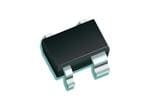
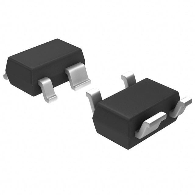
| 描述 | TRANS RF NPN 42GHZ 4.7V SOT343射频双极晶体管 RF BIP TRANSISTOR |
| 产品分类 | RF 晶体管 (BJT)分离式半导体 |
| 品牌 | Infineon Technologies |
| 产品手册 | |
| 产品图片 |
|
| rohs | 符合RoHS无铅 / 符合限制有害物质指令(RoHS)规范要求 |
| 产品系列 | 晶体管,晶体管射频,射频双极晶体管,Infineon Technologies BFP 740 H6327- |
| 数据手册 | http://www.infineon.com/dgdl/bfp740.pdf?folderId=db3a30431400ef68011425b291f205c5&fileId=db3a30431400ef6801142740c849070c |
| 产品型号 | BFP 740 H6327 |
| 不同 Ic、Vce 时的DC电流增益(hFE)(最小值) | 160 @ 25mA,3V |
| 产品种类 | 射频双极晶体管 |
| 供应商器件封装 | SOT-343 |
| 其它名称 | BFP 740 H6327DKR |
| 功率-最大值 | 160mW |
| 功率耗散 | 160 mW |
| 包装 | Digi-Reel® |
| 发射极-基极电压VEBO | 1.2 V |
| 商标 | Infineon Technologies |
| 噪声系数(dB,不同f时的典型值) | 0.5dB ~ 0.85dB @ 1.8GHz ~ 6GHz |
| 增益 | 27dB |
| 安装类型 | 表面贴装 |
| 安装风格 | SMD/SMT |
| 封装 | Reel |
| 封装/外壳 | SC-82A,SOT-343 |
| 封装/箱体 | SOT-343 |
| 工厂包装数量 | 3000 |
| 技术 | SiGe |
| 晶体管极性 | NPN |
| 晶体管类型 | Bipolar |
| 最大工作温度 | + 150 C |
| 最大工作频率 | 42 GHz |
| 最小工作温度 | - 65 C |
| 标准包装 | 1 |
| 电压-集射极击穿(最大值) | 4.7V |
| 电流-集电极(Ic)(最大值) | 30mA |
| 直流集电极/BaseGainhfeMin | 160 |
| 类型 | RF Silicon Germanium |
| 系列 | BFP740 |
| 配置 | Single Dual Emitter |
| 集电极—发射极最大电压VCEO | 4 V |
| 集电极连续电流 | 30 mA |
| 零件号别名 | BFP740H6327XTSA1 SP000750414 |
| 频率 | 42 GHz |
| 频率-跃迁 | 42GHz |


- 商务部:美国ITC正式对集成电路等产品启动337调查
- 曝三星4nm工艺存在良率问题 高通将骁龙8 Gen1或转产台积电
- 太阳诱电将投资9.5亿元在常州建新厂生产MLCC 预计2023年完工
- 英特尔发布欧洲新工厂建设计划 深化IDM 2.0 战略
- 台积电先进制程称霸业界 有大客户加持明年业绩稳了
- 达到5530亿美元!SIA预计今年全球半导体销售额将创下新高
- 英特尔拟将自动驾驶子公司Mobileye上市 估值或超500亿美元
- 三星加码芯片和SET,合并消费电子和移动部门,撤换高东真等 CEO
- 三星电子宣布重大人事变动 还合并消费电子和移动部门
- 海关总署:前11个月进口集成电路产品价值2.52万亿元 增长14.8%


PDF Datasheet 数据手册内容提取
BFP740 Low Noise Silicon Germanium Bipolar RF Transistor Data Sheet Revision 1.1, 2015-01-20 RF & Protection Devices
Edition 2015-01-20 Published by Infineon Technologies AG 81726 Munich, Germany © 2015 Infineon Technologies AG All Rights Reserved. Legal Disclaimer The information given in this document shall in no event be regarded as a guarantee of conditions or characteristics. With respect to any examples or hints given herein, any typical values stated herein and/or any information regarding the application of the device, Infineon Technologies hereby disclaims any and all warranties and liabilities of any kind, including without limitation, warranties of non-infringement of intellectual property rights of any third party. Information For further information on technology, delivery terms and conditions and prices, please contact the nearest Infineon Technologies Office (www.infineon.com). Warnings Due to technical requirements, components may contain dangerous substances. For information on the types in question, please contact the nearest Infineon Technologies Office. Infineon Technologies components may be used in life-support devices or systems only with the express written approval of Infineon Technologies, if a failure of such components can reasonably be expected to cause the failure of that life-support device or system or to affect the safety or effectiveness of that device or system. Life support devices or systems are intended to be implanted in the human body or to support and/or maintain and sustain and/or protect human life. If they fail, it is reasonable to assume that the health of the user or other persons may be endangered.
BFP740 BFP740, Low Noise Silicon Germanium Bipolar RF Transistor Revision History: 2015-01-20, Revision 1.1 Page Subjects (major changes since last revision) This data sheet replaces the revision from 2009-12-04. The reason for the new revision is to increase the information content for the circuit designer. The performance parameters are now enlisted in a table containing many relevant application frequencies. The measurements of typical devices have been repeated and the device description has been expanded by adding several new characteristic curves. For customers who bought the product prior to the issue of the new revision the old specifications remain valid. Trademarks of Infineon Technologies AG AURIX™, C166™, CanPAK™, CIPOS™, CIPURSE™, EconoPACK™, CoolMOS™, CoolSET™, CORECONTROL™, CROSSAVE™, DAVE™, DI-POL™, EasyPIM™, EconoBRIDGE™, EconoDUAL™, EconoPIM™, EconoPACK™, EiceDRIVER™, eupec™, FCOS™, HITFET™, HybridPACK™, I²RF™, ISOFACE™, IsoPACK™, MIPAQ™, ModSTACK™, my-d™, NovalithIC™, OptiMOS™, ORIGA™, POWERCODE™; PRIMARION™, PrimePACK™, PrimeSTACK™, PRO-SIL™, PROFET™, RASIC™, ReverSave™, SatRIC™, SIEGET™, SINDRION™, SIPMOS™, SmartLEWIS™, SOLIDFLASH™, TEMPFET™, thinQ!™, TRENCHSTOP™, TriCore™. Other Trademarks Advance Design System™ (ADS) of Agilent Technologies, AMBA™, ARM™, MULTI-ICE™, KEIL™, PRIMECELL™, REALVIEW™, THUMB™, µVision™ of ARM Limited, UK. AUTOSAR™ is licensed by AUTOSAR development partnership. Bluetooth™ of Bluetooth SIG Inc. CAT-iq™ of DECT Forum. COLOSSUS™, FirstGPS™ of Trimble Navigation Ltd. EMV™ of EMVCo, LLC (Visa Holdings Inc.). EPCOS™ of Epcos AG. FLEXGO™ of Microsoft Corporation. FlexRay™ is licensed by FlexRay Consortium. HYPERTERMINAL™ of Hilgraeve Incorporated. IEC™ of Commission Electrotechnique Internationale. IrDA™ of Infrared Data Association Corporation. ISO™ of INTERNATIONAL ORGANIZATION FOR STANDARDIZATION. MATLAB™ of MathWorks, Inc. MAXIM™ of Maxim Integrated Products, Inc. MICROTEC™, NUCLEUS™ of Mentor Graphics Corporation. MIPI™ of MIPI Alliance, Inc. MIPS™ of MIPS Technologies, Inc., USA. muRata™ of MURATA MANUFACTURING CO., MICROWAVE OFFICE™ (MWO) of Applied Wave Research Inc., OmniVision™ of OmniVision Technologies, Inc. Openwave™ Openwave Systems Inc. RED HAT™ Red Hat, Inc. RFMD™ RF Micro Devices, Inc. SIRIUS™ of Sirius Satellite Radio Inc. SOLARIS™ of Sun Microsystems, Inc. SPANSION™ of Spansion LLC Ltd. Symbian™ of Symbian Software Limited. TAIYOYUDEN™ of Taiyo Yuden Co. TEAKLITE™ of CEVA, Inc. TEKTRONIX™ of Tektronix Inc. TOKO™ of TOKO KABUSHIKI KAISHA TA. UNIX™ of X/Open Company Limited. VERILOG™, PALLADIUM™ of Cadence Design Systems, Inc. VLYNQ™ of Texas Instruments Incorporated. VXWORKS™, WIND RIVER™ of WIND RIVER SYSTEMS, INC. ZETEX™ of Diodes Zetex Limited. Last Trademarks Update 2011-11-11 Data Sheet 3 Revision 1.1, 2015-01-20
BFP740 Table of Contents Table of Contents Table of Contents . . . . . . . . . . . . . . . . . . . . . . . . . . . . . . . . . . . . . . . . . . . . . . . . . . . . . . . . . . . . . . . . 4 List of Figures . . . . . . . . . . . . . . . . . . . . . . . . . . . . . . . . . . . . . . . . . . . . . . . . . . . . . . . . . . . . . . . . . . . 5 List of Tables . . . . . . . . . . . . . . . . . . . . . . . . . . . . . . . . . . . . . . . . . . . . . . . . . . . . . . . . . . . . . . . . . . . . 6 1 Product Brief . . . . . . . . . . . . . . . . . . . . . . . . . . . . . . . . . . . . . . . . . . . . . . . . . . . . . . . . . . . . . . . . . . . . 7 2 Features . . . . . . . . . . . . . . . . . . . . . . . . . . . . . . . . . . . . . . . . . . . . . . . . . . . . . . . . . . . . . . . . . . . . . . . . 8 3 Maximum Ratings . . . . . . . . . . . . . . . . . . . . . . . . . . . . . . . . . . . . . . . . . . . . . . . . . . . . . . . . . . . . . . . . 9 4 Thermal Characteristics . . . . . . . . . . . . . . . . . . . . . . . . . . . . . . . . . . . . . . . . . . . . . . . . . . . . . . . . . . 10 5 Electrical Characteristics . . . . . . . . . . . . . . . . . . . . . . . . . . . . . . . . . . . . . . . . . . . . . . . . . . . . . . . . . 11 5.1 DC Characteristics . . . . . . . . . . . . . . . . . . . . . . . . . . . . . . . . . . . . . . . . . . . . . . . . . . . . . . . . . . . . . . . 11 5.2 General AC Characteristics . . . . . . . . . . . . . . . . . . . . . . . . . . . . . . . . . . . . . . . . . . . . . . . . . . . . . . . . 11 5.3 Frequency Dependent AC Characteristics . . . . . . . . . . . . . . . . . . . . . . . . . . . . . . . . . . . . . . . . . . . . . 12 5.4 Characteristic DC Diagrams . . . . . . . . . . . . . . . . . . . . . . . . . . . . . . . . . . . . . . . . . . . . . . . . . . . . . . . . 16 5.5 Characteristic AC Diagrams . . . . . . . . . . . . . . . . . . . . . . . . . . . . . . . . . . . . . . . . . . . . . . . . . . . . . . . . 19 6 Simulation Data . . . . . . . . . . . . . . . . . . . . . . . . . . . . . . . . . . . . . . . . . . . . . . . . . . . . . . . . . . . . . . . . . 26 7 Package Information SOT343 . . . . . . . . . . . . . . . . . . . . . . . . . . . . . . . . . . . . . . . . . . . . . . . . . . . . . 27 Data Sheet 4 Revision 1.1, 2015-01-20
BFP740 List of Figures List of Figures Figure4-1 Total Power Dissipation P = f(T ). . . . . . . . . . . . . . . . . . . . . . . . . . . . . . . . . . . . . . . . . . . . . . . . 10 tot S Figure5-1 BFP740 Testing Circuit. . . . . . . . . . . . . . . . . . . . . . . . . . . . . . . . . . . . . . . . . . . . . . . . . . . . . . . . . . 12 Figure5-2 Collector Current vs. Collector Emitter Voltage I =f(V ), I =Parameter in µA. . . . . . . . . . . . . 16 C CE B Figure5-3 DC Current Gain h =f(I ), V =3V . . . . . . . . . . . . . . . . . . . . . . . . . . . . . . . . . . . . . . . . . . . . . 16 FE C CE Figure5-4 Collector Current vs. Base Emitter Forward Voltage I =f(V ), V =2V . . . . . . . . . . . . . . . . . 17 C BE CE Figure5-5 Base Current vs. Base Emitter Forward Voltage I =f (V ), V =2V . . . . . . . . . . . . . . . . . . . . 17 B BE CE Figure5-6 Base Current vs. Base Emitter Reverse Voltage I =f(V ), V =2V . . . . . . . . . . . . . . . . . . . . 18 B EB CE Figure5-7 Transition Frequency f =f(I ), V =Parameter in V. . . . . . . . . . . . . . . . . . . . . . . . . . . . . . . . . . 19 T C CE Figure5-8 3rd Order Intercept Point at output OIP3=f(I ), Z =Z =50 Ω, V f=Parameters. . . . . . . . . 19 C S L CE, Figure5-9 3rd Order Intercept Point at output OIP3 [dBm] = f (I V ), Z = Z = 50 Ω, f = 5.5 GHz . . . . . . 20 C, CE S L Figure5-10 Compression Point at output OP [dBm] = f(I V ), Z = Z = 50 Ω, f = 5.5 GHz . . . . . . . . . . 20 1dB C, CE S L Figure5-11 Collector Base Capacitance C = f (V ), f=1 MHz . . . . . . . . . . . . . . . . . . . . . . . . . . . . . . . . . . 21 CB CB Figure5-12 Gain G G |S |2 = f (f), V = 3 V, I = 15 mA . . . . . . . . . . . . . . . . . . . . . . . . . . . . . . . . . . . . . 21 ma, ms, 21 CE C Figure5-13 Maximum Power Gain G = f (I ), V = 3 V, f = Parameter in GHz. . . . . . . . . . . . . . . . . . . . . . 22 max C CE Figure5-14 Maximum Power Gain G = f (V ), I = 15 mA, f = Parameter in GHz . . . . . . . . . . . . . . . . . . . 22 max CE C Figure5-15 Input Matching S = f (f), V = 3V, I = 6 / 15 mA . . . . . . . . . . . . . . . . . . . . . . . . . . . . . . . . . . . 23 11 CE C Figure5-16 Source Impedance for Minimum Noise Figure Z = f (f), V = 3V, I = 6 / 15 mA. . . . . . . . . . . 23 opt CE C Figure5-17 Output Matching S = f (f), V = 3V, I = 6 / 15 mA . . . . . . . . . . . . . . . . . . . . . . . . . . . . . . . . . . 24 22 CE C Figure5-18 Noise Figure NF = f (f), V = 3 V, I = 6 / 15 mA, Z = Z . . . . . . . . . . . . . . . . . . . . . . . . . . . 24 min CE C S opt Figure5-19 Noise Figure NF = f (I ), V = 3 V, Z = Z , f = Parameter in GHz. . . . . . . . . . . . . . . . . . . . . 25 min C CE S opt Figure5-20 Noise Figure NF = f (I ), V = 3 V, Z = 50 Ω, f = Parameter in GHz . . . . . . . . . . . . . . . . . . . . 25 50 C CE S Figure7-1 Package Outline. . . . . . . . . . . . . . . . . . . . . . . . . . . . . . . . . . . . . . . . . . . . . . . . . . . . . . . . . . . . . . . 27 Figure7-2 Package Footprint. . . . . . . . . . . . . . . . . . . . . . . . . . . . . . . . . . . . . . . . . . . . . . . . . . . . . . . . . . . . . . 27 Figure7-3 Marking Description (Marking BFP740: R7s). . . . . . . . . . . . . . . . . . . . . . . . . . . . . . . . . . . . . . . . . 27 Figure7-4 Tape Dimensions . . . . . . . . . . . . . . . . . . . . . . . . . . . . . . . . . . . . . . . . . . . . . . . . . . . . . . . . . . . . . . 27 Data Sheet 5 Revision 1.1, 2015-01-20
BFP740 List of Tables List of Tables Table3-1 Maximum Ratings at T = 25 °C (unless otherwise specified) . . . . . . . . . . . . . . . . . . . . . . . . . . . . . 9 A Table4-1 Thermal Resistance . . . . . . . . . . . . . . . . . . . . . . . . . . . . . . . . . . . . . . . . . . . . . . . . . . . . . . . . . . . . 10 Table5-1 DC Characteristics at T = 25 °C . . . . . . . . . . . . . . . . . . . . . . . . . . . . . . . . . . . . . . . . . . . . . . . . . 11 A Table5-2 General AC Characteristics at T = 25°C . . . . . . . . . . . . . . . . . . . . . . . . . . . . . . . . . . . . . . . . . . . 11 A Table5-3 AC Characteristics, V =3V, f=0.45GHz . . . . . . . . . . . . . . . . . . . . . . . . . . . . . . . . . . . . . . . . . 13 CE Table5-4 AC Characteristics, V =3V, f=0.9GHz . . . . . . . . . . . . . . . . . . . . . . . . . . . . . . . . . . . . . . . . . . 13 CE Table5-5 AC Characteristics, V =3V, f=1.5GHz . . . . . . . . . . . . . . . . . . . . . . . . . . . . . . . . . . . . . . . . . . 13 CE Table5-6 AC Characteristics, V =3V, f=1.9GHz . . . . . . . . . . . . . . . . . . . . . . . . . . . . . . . . . . . . . . . . . . 14 CE Table5-7 AC Characteristics, V =3V, f=2.4GHz . . . . . . . . . . . . . . . . . . . . . . . . . . . . . . . . . . . . . . . . . . 14 CE Table5-8 AC Characteristics, V =3V, f=3.5GHz . . . . . . . . . . . . . . . . . . . . . . . . . . . . . . . . . . . . . . . . . . 14 CE Table5-9 AC Characteristics, V =3V, f=5.5GHz . . . . . . . . . . . . . . . . . . . . . . . . . . . . . . . . . . . . . . . . . . 15 CE Data Sheet 6 Revision 1.1, 2015-01-20
BFP740 Product Brief 1 Product Brief The BFP740 is a linear very low noise wideband NPN bipolar RF transistor. The device is based on Infineon’s reliable high volume silicon germanium carbon (SiGe:C) heterojunction bipolar technology. The collector design supports voltages up to V = 4.0 V and currents up to I = 45 mA. With its high linearity at currents as low as 10 CEO C mA (see Fig. 5-8) the device supports energy efficient designs. The typical transition frequency is approximately 45 GHz, hence the device offers high power gain at frequencies up to 11 GHz in amplifier applications. The device is housed in an easy to use plastic package with visible leads. Data Sheet 7 Revision 1.1, 2015-01-20
BFP740 Features 2 Features • Very low noise amplifier based on Infineon´s reliable, high volume SiGe:C technology • OIP3= 24.5 dBm @ 5.5 GHz, 3 V, 15 mA • High transition frequency f = 44 GHz @ 3 V, 25 mA T • NF = 0.85 dB @ 5.5 GHz, 3 V, 6 mA 3 min • Maximum power gain Gms = 19.5 dB @ 5.5 GHz, 3 V, 15 mA 2 4 • Low power consumption, ideal for mobile applications, 1 very common in WLAN Wi-Fi applications • Easy to use Pb-free (RoHS compliant) and halogen-free standard package with visible leads • Qualification report according to AEC-Q101 available Applications As Low Noise Amplifier (LNA) in • Mobile, portable and fixed connectivity applications: WLAN 802.11a/b/g/n/ac, WiMAX 2.5/3.5/5.5 GHz, UWB, Bluetooth • Satellite communication systems: Navigation systems (GPS, Glonass), satellite radio (SDARs, DAB) and C-band LNB • Multimedia applications such as mobile/portable TV, CATV, FM Radio • 3G/4G UMTS/LTE mobile phone applications • ISM applications like RKE, AMR and Zigbee, as well as for emerging wireless applications As discrete active mixer, amplifier in VCOs and buffer amplifier Attention:ESD (Electrostatic discharge) sensitive device, observe handling precautions Product Name Package Pin Configuration Marking BFP740 SOT343 1 = B 2 = E 3 = C 4 = E R7s Data Sheet 8 Revision 1.1, 2015-01-20
BFP740 Maximum Ratings 3 Maximum Ratings Table3-1 Maximum Ratings at T = 25 °C (unless otherwise specified) A Parameter Symbol Values Unit Note / TestCondition Min. Max. Collector emitter voltage V V Open base CEO – 4.0 T = 25 °C A – 3.5 T = -55 °C A Collector emitter voltage V – 13 V E-B short circuited CES Collector base voltage V – 13 V Open emitter CBO Emitter base voltage V – 1.2 V Open collector EBO Collector current I – 45 mA – C Base current I – 4 mA – B Total power dissipation1) P – 160 mW T ≤ 100 °C tot S Junction temperature T – 150 °C – J Storage temperature T -55 150 °C – Stg 1) T is the soldering point temperature. T is measured on the emitter lead at the soldering point of the pcb. S S Attention:Stresses above the max. values listed here may cause permanent damage to the device. Exposure to absolute maximum rating conditions for extended periods may affect device reliability. Maximum ratings are absolute ratings; exceeding only one of these values may cause irreversible damage to the integrated circuit. Data Sheet 9 Revision 1.1, 2015-01-20
BFP740 Thermal Characteristics 4 Thermal Characteristics Table4-1 Thermal Resistance Parameter Symbol Values Unit Note / TestCondition Min. Typ. Max. Junction - soldering point1) R – – 310 K/W – thJS 1)For the definition of R please refer to Application Note AN077 (Thermal Resistance Calculation) thJS 180 160 140 120 W] 100 m [ot 80 Pt 60 40 20 0 0 25 50 75 100 125 150 T [°C] S Figure4-1 Total Power Dissipation P = f(T ) tot S Data Sheet 10 Revision 1.1, 2015-01-20
BFP740 Electrical Characteristics 5 Electrical Characteristics 5.1 DC Characteristics Table5-1 DC Characteristics at T = 25 °C A Parameter Symbol Values Unit Note / TestCondition Min. Typ. Max. Collector emitter breakdown voltage V 4 4.7 – V I =1mA, I =0 (BR)CEO C B Open base Collector emitter leakage current I – 1 4001) nA V =13 V, V =0 CES CE BE 1 401) V =5 V, V =0 CE BE E-B short circuited Collector base leakage current I – 1 401) nA V =5V, I =0 CBO CB E Open emitter Emitter base leakage current I – 1 401) nA V =0.5V, I =0 EBO EB C Open collector DC current gain h 160 250 400 V =3V, I = 25mA FE CE C Pulse measured 1) Maximum values not limited by the device but by the short cycle time ot the 100% test 5.2 General AC Characteristics Table5-2 General AC Characteristics at T = 25°C A Parameter Symbol Values Unit Note / TestCondition Min. Typ. Max. Transition frequency f – 44 – GHz V =3V, I =25mA T CE C f=2 GHz Collector base capacitance C – 0.08 – pF V =3V, V =0 CB CB BE f=1MHz Emitter grounded Collector emitter capacitance C – 0.35 – pF V =3V, V =0 CE CE BE f=1MHz Base grounded Emitter base capacitance C – 0.45 – pF V =0.5V,V =0 EB EB CB f=1MHz Collector grounded Data Sheet 11 Revision 1.1, 2015-01-20
BFP740 Electrical Characteristics 5.3 Frequency Dependent AC Characteristics Measurement setup is a test fixture with Bias T´s in a 50 Ω system, T =25°C A VC Top View Bias-T OUT E C VB B E Bias-T (Pin 1) IN Figure5-1 BFP740 Testing Circuit Data Sheet 12 Revision 1.1, 2015-01-20
BFP740 Electrical Characteristics Table5-3 AC Characteristics, V =3V, f=0.45GHz CE Parameter Symbol Values Unit Note / TestCondition Min. Typ. Max. Power Gain dB Maximum power gain G – 31.5 – I =15mA ms C Transducer gain |S |2 – 28.5 – I =15mA 21 C Minimum Noise Figure dB Minimum noise figure NF – 0.45 – I =6mA min C Associated gain G – 26 – I =6mA ass C Linearity dBm Z =Z =50Ω S L 1 dB compression point at output OP – 6.5 – I =15mA 1dB C 3rd order intercept point at output OIP3 – 22 – I =15mA C Table5-4 AC Characteristics, V =3V, f=0.9GHz CE Parameter Symbol Values Unit Note / TestCondition Min. Typ. Max. Power Gain dB Maximum power gain G – 28 – I =15mA ms C Transducer gain |S |2 – 27 – I =15mA 21 C Minimum Noise Figure dB Minimum noise figure NF – 0.45 – I =6mA min C Associated gain G – 24.5 – I =6mA ass C Linearity dBm Z =Z =50Ω S L 1 dB compression point at output OP – 8 – I =15mA 1dB C 3rd order intercept point at output OIP3 – 22.5 – I =15mA C Table5-5 AC Characteristics, V =3V, f=1.5GHz CE Parameter Symbol Values Unit Note / TestCondition Min. Typ. Max. Power Gain dB Maximum power gain G – 26 – I =15mA ms C Transducer gain |S |2 – 25 – I =15mA 21 C Minimum Noise Figure dB Minimum noise figure NF – 0.5 – I =6mA min C Associated gain G – 22.5 – I =6mA ass C Linearity dBm Z =Z =50Ω S L 1 dB compression point at output OP – 7 – I =15mA 1dB C 3rd order intercept point at output OIP3 – 23 – I =15mA C Data Sheet 13 Revision 1.1, 2015-01-20
BFP740 Electrical Characteristics Table5-6 AC Characteristics, V =3V, f=1.9GHz CE Parameter Symbol Values Unit Note / TestCondition Min. Typ. Max. Power Gain dB Maximum power gain G – 25 – I =15mA ms C Transducer gain |S |2 – 23.5 – I =15mA 21 C Minimum Noise Figure dB Minimum noise figure NF – 0.5 – I =6mA min C Associated gain G – 21.5 – I =6mA ass C Linearity dBm Z =Z =50Ω S L 1 dB compression point at output OP – 9 – I =15mA 1dB C 3rd order intercept point at output OIP3 – 24.5 – I =15mA C Table5-7 AC Characteristics, V =3V, f=2.4GHz CE Parameter Symbol Values Unit Note / TestCondition Min. Typ. Max. Power Gain dB Maximum power gain G – 24 – I =15mA ms C Transducer gain |S |2 – 22 – I =15mA 21 C Minimum Noise Figure dB Minimum noise figure NF – 0.55 – I =6mA min C Associated gain G – 20 – I =6mA ass C Linearity dBm Z =Z =50Ω S L 1 dB compression point at output OP – 8 – I =15mA 1dB C 3rd order intercept point at output OIP3 – 24.5 – I =15mA C Table5-8 AC Characteristics, V =3V, f=3.5GHz CE Parameter Symbol Values Unit Note / TestCondition Min. Typ. Max. Power Gain dB Maximum power gain G – 22 – I =15mA ms C Transducer gain |S |2 – 19 – I =15mA 21 C Minimum Noise Figure dB Minimum noise figure NF – 0.65 – I =6mA min C Associated gain G – 17 – I =6mA ass C Linearity dBm Z =Z =50Ω S L 1 dB compression point at output OP – 9 – I =15mA 1dB C 3rd order intercept point at output OIP3 – 25.5 – I =15mA C Data Sheet 14 Revision 1.1, 2015-01-20
BFP740 Electrical Characteristics Table5-9 AC Characteristics, V =3V, f=5.5GHz CE Parameter Symbol Values Unit Note / TestCondition Min. Typ. Max. Power Gain dB Maximum power gain G – 19.5 – I =15mA ms C Transducer gain |S |2 – 15 – I =15mA 21 C Minimum Noise Figure dB Minimum noise figure NF – 0.85 – I =6mA min C Associated gain G – 14 – I =6mA ass C Linearity dBm Z =Z =50Ω S L 1 dB compression point at output OP – 9 – I =15mA 1dB C 3rd order intercept point at output OIP3 – 24.5 – I =15mA C Note:OIP3 value depends on termination of all intermodulation frequency components. Termination used for this measurement is 50 Ω from 0.2 MHz to 12 GHz. Data Sheet 15 Revision 1.1, 2015-01-20
BFP740 Electrical Characteristics 5.4 Characteristic DC Diagrams 26 24 100μA 22 90μA 20 80μA 70μA 18 60μA 16 A] 14 50μA m [C 12 40μA I 10 30μA 8 20μA 6 4 10μA 2 0 0 1 2 3 4 5 V [V] CE Figure5-2 Collector Current vs. Collector Emitter Voltage I =f(V ), I =Parameter in µA C CE B 3 10 E F h 2 10 0 1 2 10 10 10 I [mA] C Figure5-3 DC Current Gain h =f(I ), V =3V FE C CE Data Sheet 16 Revision 1.1, 2015-01-20
BFP740 Electrical Characteristics 2 10 1 10 0 10 A] m 10−1 [C I −2 10 −3 10 −4 10 0.5 0.55 0.6 0.65 0.7 0.75 0.8 0.85 0.9 V [V] BE Figure5-4 Collector Current vs. Base Emitter Forward Voltage I =f(V ), V =2V C BE CE 0 10 −1 10 −2 10 −3 10 A] m [B −4 I 10 −5 10 −6 10 −7 10 0.5 0.55 0.6 0.65 0.7 0.75 0.8 0.85 0.9 V [V] BE Figure5-5 Base Current vs. Base Emitter Forward Voltage I =f (V ), V =2V B BE CE Data Sheet 17 Revision 1.1, 2015-01-20
BFP740 Electrical Characteristics −9 10 −10 10 −11 10 A] [B I −12 10 −13 10 −14 10 0.8 0.9 1 1.1 1.2 V [V] EB Figure5-6 Base Current vs. Base Emitter Reverse Voltage I =f(V ), V =2V B EB CE Data Sheet 18 Revision 1.1, 2015-01-20
BFP740 Electrical Characteristics 5.5 Characteristic AC Diagrams Measurement setup is a test fixture with Bias T´s in a 50 Ω system, T =25°C. A 48 44 4.00V 40 36 3.50V 32 3.00V 28 z] H G 24 [T f 20 2.50V 16 12 2.00V 8 4 1.00V 0 0 10 20 30 40 50 IC [mA] Figure5-7 Transition Frequency f =f(I ), V =Parameter in V T C CE 26 24 22 20 18 16 m] B 14 d [3 12 P OI 10 8 2V, 2400MHz 6 3V, 2400MHz 2V, 5500MHz 4 3V, 5500MHz 2 0 0 5 10 15 20 25 30 I [mA] C Figure5-8 3rd Order Intercept Point at output OIP3=f(I ), Z =Z =50 Ω, V f=Parameters C S L CE, Data Sheet 19 Revision 1.1, 2015-01-20
BFP740 Electrical Characteristics 25 678910111213141516171819 20 2122 23 24 25 26 6 20 2 2 mA] 15113141516171819 2021 22 23 24 25 [C I 10 2 4 25 141516171819 20 21 22 23 24 23 22 21 21 20 19 20 5 1 1.5 2 2.5 3 3.5 4 V [V] CE Figure5-9 3rd Order Intercept Point at output OIP3 [dBm] = f (I V ), Z = Z = 50 Ω, f = 5.5 GHz C, CE S L 25 7 9 0 1 12 1 1 20 8 11 10 9 10 8 A] 9 m 15 9 I [C 7 8 8 8 7 7 6 6 6 6 10 5 5 5 5 4 4 4 4 3 3 3 3 2 2 2 2 1 1 1 1 0 0 0 0 5 −1 2 2.5 3 3.5 4 V [V] CE Figure5-10 Compression Point at output OP [dBm] = f(I V ), Z = Z = 50 Ω, f = 5.5 GHz 1dB C, CE S L Data Sheet 20 Revision 1.1, 2015-01-20
BFP740 Electrical Characteristics 0.2 0.16 0.12 F] p [B C C 0.08 0.04 0 0 0.5 1 1.5 2 2.5 3 3.5 4 V [V] CB Figure5-11 Collector Base Capacitance C = f (V ), f=1 MHz CB CB 40 35 30 G ms 25 B] d 20 G [ |S |2 G 21 ma 15 10 5 0 0 1 2 3 4 5 6 7 8 9 10 f [GHz] Figure5-12 Gain G G |S |2 = f (f), V = 3 V, I = 15 mA ma, ms, 21 CE C Data Sheet 21 Revision 1.1, 2015-01-20
BFP740 Electrical Characteristics 40 0.15GHz 35 0.45GHz 30 0.90GHz 1.50GHz 1.90GHz 25 2.40GHz B] d 3.50GHz [x 20 a m 5.50GHz G 15 10.00GHz 10 5 0 0 5 10 15 20 25 30 35 40 45 50 55 I [mA] C Figure5-13 Maximum Power Gain G = f (I ), V = 3 V, f = Parameter in GHz max C CE 40 0.15GHz 35 0.45GHz 30 0.90GHz 1.50GHz 25 1.90GHz B] 2.40GHz d 3.50GHz [ax 20 5.50GHz m G 15 10.00GHz 10 5 0 0 0.5 1 1.5 2 2.5 3 3.5 4 4.5 5 V [V] CE Figure5-14 Maximum Power Gain G = f (V ), I = 15 mA, f = Parameter in GHz max CE C Data Sheet 22 Revision 1.1, 2015-01-20
BFP740 Electrical Characteristics 1 1.5 0.5 10.0 2 9.0 0.4 8.0 9.0 10.0 8.0 3 0.3 7.0 7.0 6.0 4 6.0 0.2 5 5.0 0.03 to 10 GHz 5.0 0.1 4.0 10 0.1 0.2 0.3 0.40.5 1 1.5 2 3 4 5 0 4.0 0.03 0.03 3.0 −0.1 −10 −0.2 3.0 2.0 −5 −4 −0.3 1.0 −3 −0.4 2.0 1.0 −0.5 −2 −1.5 −1 6.0mA 15mA Figure5-15 Input Matching S = f (f), V = 3V, I = 6 / 15 mA 11 CE C 1 1.5 0.5 2 0.4 3 0.3 0.45 to 10 GHz 4 0.2 5 3.5 2.4 0.1 4.5 1.9 10 1.5 0.1 0.2 0.3 0.40.55.5 4.5 31.52.4111.9..55 2 00..4935 4 5 0 0.9 0.45 5.5 −0.1 8.0 −10 8.0 −0.2 10.0 −5 −4 −0.3 10.0 −3 −0.4 −0.5 −2 6mA −1.5 −1 15mA Figure5-16 Source Impedance for Minimum Noise Figure Z = f (f), V = 3V, I = 6 / 15 mA opt CE C Data Sheet 23 Revision 1.1, 2015-01-20
BFP740 Electrical Characteristics 1 1.5 0.5 2 0.4 3 0.3 10.0 4 10.0 0.2 5 9.0 9.0 0.03 to 10 GHz 8.0 0.1 8.0 10 7.0 7.0 6.0 0.1 0.2 0.3 0.40.5 1 1.5 2 3 4 5 0 6.0 5.0 0.03 0.03 4.0 −0.1 5.0 −10 3.0 4.0 −0.2 2.0 −5 1.0 −4 −0.3 3.0 1.0 −3 2.0 −0.4 −0.5 −2 −1.5 −1 6.0mA 15mA Figure5-17 Output Matching S = f (f), V = 3V, I = 6 / 15 mA 22 CE C 1.8 1.6 1.4 1.2 B] 1 d [n mi F 0.8 N 0.6 I = 15mA 0.4 C I = 6.0mA C 0.2 0 0 1 2 3 4 5 6 7 8 9 10 f [GHz] Figure5-18 Noise Figure NF = f (f), V = 3 V, I = 6 / 15 mA, Z = Z min CE C S opt Data Sheet 24 Revision 1.1, 2015-01-20
BFP740 Electrical Characteristics 2.4 f = 10GHz 2.2 f = 5.5GHz 2 f = 3.5GHz 1.8 f = 2.4GHz f = 1.9GHz 1.6 f = 1.5GHz B] 1.4 f = 0.9GHz d [n 1.2 f = 0.45GHz mi F N 1 0.8 0.6 0.4 0.2 0 0 5 10 15 20 25 I [mA] C Figure5-19 Noise Figure NF = f (I ), V = 3 V, Z = Z , f = Parameter in GHz min C CE S opt 3.6 3.4 3.2 3 f = 10GHz 2.8 f = 5.5GHz 2.6 f = 3.5GHz 2.4 f = 2.4GHz 2.2 f = 1.9GHz B] 2 f = 1.5GHz d [0 1.8 f = 0.9GHz 5 F 1.6 f = 0.45GHz N 1.4 1.2 1 0.8 0.6 0.4 0.2 0 0 5 10 15 20 25 I [mA] C Figure5-20 Noise Figure NF = f (I ), V = 3 V, Z = 50 Ω, f = Parameter in GHz 50 C CE S Note:The curves shown in this chapter have been generated using typical devices but shall not be considered as a guarantee that all devices have identical characteristic curves. Data Sheet 25 Revision 1.1, 2015-01-20
BFP740 Simulation Data 6 Simulation Data For the SPICE Gummel Poon (GP) model as well as for the S-parameters (including noise parameters) please refer to our internet website. Please consult our website and download the latest versions before actually starting your design. You find the BFP740 SPICE GP model in the internet in MWO- and ADS-format, which you can import into these circuit simulation tools very quickly and conveniently. The model already contains the package parasitics and is ready to use for DC and high frequency simulations. The terminals of the model circuit correspond to the pin configuration of the device. The model parameters have been extracted and verified up to 10 GHz using typical devices. The BFP740 SPICE GP model reflects the typical DC- and RF-performance within the limitations which are given by the SPICE GP model itself. Besides the DC characteristics all S-parameters in magnitude and phase, as well as noise figure (including optimum source impedance, equivalent noise resistance and flicker noise) and intermodulation have been extracted. Data Sheet 26 Revision 1.1, 2015-01-20
BFP740 Package Information SOT343 7 Package Information SOT343 0.9±0.1 2±0.2 0.1 MAX. 1.3 0.1 A 4 3 0.15 2.1±0.1 MIN. 1.25±0.1 1 1 2 0. 0.3+-00..015 0.15+-00..015 4x 0.6+-00..015 0.1M 0.2M A SOT343-PO V08 Figure7-1 Package Outline 0.6 8 0. 6 1. 1.15 0.9 SOT343-FP V08 Figure7-2 Package Footprint Type code XYs Date code (YM) 6 Manufacturer 2005, June 5 Pin 1 Figure7-3 Marking Description (Marking BFP740: R7s) 4 0.2 8 3 2. Pin 1 2.15 1.1 SOT323-TP V02 Figure7-4 Tape Dimensions Data Sheet 27 Revision 1.1, 2015-01-20
w w w . i n f i n e o n . c o m Published by Infineon Technologies AG
Mouser Electronics Authorized Distributor Click to View Pricing, Inventory, Delivery & Lifecycle Information: I nfineon: BFP 740 H6327 BFP 740 E6327 BFP740H6327XTSA1