ICGOO在线商城 > 分立半导体产品 > 晶体管 - FET,MOSFET - 射频 > BF512,215
 Datasheet下载
- 型号: BF512,215
- 制造商: NXP Semiconductors
- 库位|库存: xxxx|xxxx
- 要求:
| 数量阶梯 | 香港交货 | 国内含税 |
| +xxxx | $xxxx | ¥xxxx |
查看当月历史价格
查看今年历史价格
BF512,215产品简介:
ICGOO电子元器件商城为您提供BF512,215由NXP Semiconductors设计生产,在icgoo商城现货销售,并且可以通过原厂、代理商等渠道进行代购。 BF512,215价格参考。NXP SemiconductorsBF512,215封装/规格:晶体管 - FET,MOSFET - 射频, RF Mosfet N-Channel JFET 10V 5mA 100MHz TO-236AB (SOT23)。您可以下载BF512,215参考资料、Datasheet数据手册功能说明书,资料中有BF512,215 详细功能的应用电路图电压和使用方法及教程。
| 参数 | 数值 |
| 产品目录 | |
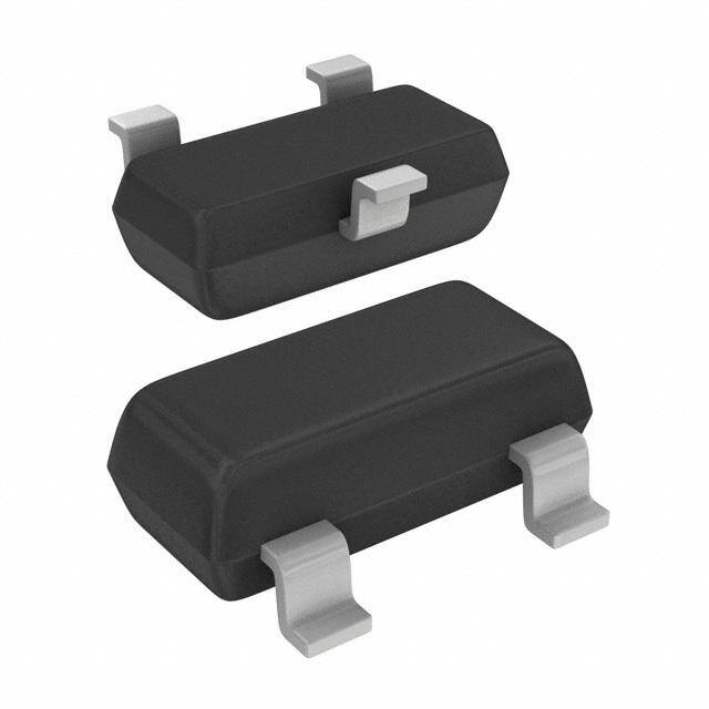
| 描述 | JFET N-CH 20V 30MA SOT23射频JFET晶体管 TAPE7 FET-RFSS |
| 产品分类 | RF FET分离式半导体 |
| Id-连续漏极电流 | 12 mA |
| 品牌 | NXP Semiconductors |
| 产品手册 | |
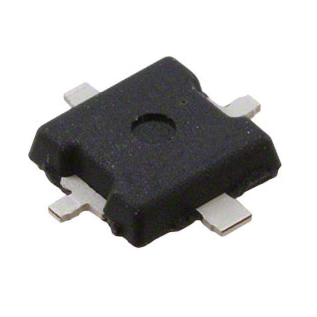
| 产品图片 |
|
| rohs | 符合RoHS无铅 / 符合限制有害物质指令(RoHS)规范要求 |
| 产品系列 | 晶体管,晶体管射频,射频JFET晶体管,NXP Semiconductors BF512,215- |
| 数据手册 | |
| 产品型号 | BF512,215 |
| PCN封装 | |
| PCN设计/规格 | |
| Pd-PowerDissipation | 250 mW |
| Pd-功率耗散 | 250 mW |
| Vds-Drain-SourceBreakdownVoltage | 20 V |
| Vds-漏源极击穿电压 | 20 V |
| Vgs-Gate-SourceBreakdownVoltage | 20 V |
| Vgs-栅源极击穿电压 | 20 V |
| Vgs=0时的漏-源电流 | 6 mA to 12 mA |
| 产品 | RF JFET |
| 产品种类 | 射频JFET晶体管 |
| 供应商器件封装 | SOT-23 (TO-236AB) |
| 其它名称 | 568-6162-1 |
| 功率-输出 | - |
| 功率耗散 | 250 mW |
| 包装 | 剪切带 (CT) |
| 商标 | NXP Semiconductors |
| 噪声系数 | 1.5dB |
| 增益 | - |
| 安装风格 | SMD/SMT |
| 封装 | Reel |
| 封装/外壳 | TO-236-3,SC-59,SOT-23-3 |
| 封装/箱体 | SOT-23 |
| 工厂包装数量 | 3000 |
| 技术 | Silicon |
| 晶体管极性 | N-Channel |
| 晶体管类型 | JFET |
| 最大工作温度 | + 150 C |
| 最大漏极/栅极电压 | 20 V |
| 标准包装 | 1 |
| 漏源电压VDS | 20 V |
| 电压-测试 | 10V |
| 电压-额定 | 20V |
| 电流-测试 | 5mA |
| 类型 | Silicon |
| 配置 | Single |
| 闸/源击穿电压 | 20 V |
| 闸/源截止电压 | 2.2 V |
| 零件号别名 | BF512 T/R |
| 频率 | 100MHz |
| 额定电流 | 30mA |


- 商务部:美国ITC正式对集成电路等产品启动337调查
- 曝三星4nm工艺存在良率问题 高通将骁龙8 Gen1或转产台积电
- 太阳诱电将投资9.5亿元在常州建新厂生产MLCC 预计2023年完工
- 英特尔发布欧洲新工厂建设计划 深化IDM 2.0 战略
- 台积电先进制程称霸业界 有大客户加持明年业绩稳了
- 达到5530亿美元!SIA预计今年全球半导体销售额将创下新高
- 英特尔拟将自动驾驶子公司Mobileye上市 估值或超500亿美元
- 三星加码芯片和SET,合并消费电子和移动部门,撤换高东真等 CEO
- 三星电子宣布重大人事变动 还合并消费电子和移动部门
- 海关总署:前11个月进口集成电路产品价值2.52万亿元 增长14.8%

PDF Datasheet 数据手册内容提取
DISCRETE SEMICONDUCTORS DATA SHEET BF510 to 513 N-channel silicon field-effect transistors Product specification December 1997
NXP Semiconductors Product specification N-channel silicon field-effect transistors BF510 to 513 DESCRIPTION MARKING CODE Asymmetrical N-channel planar BF510=S6p epitaxial junction field-effect BF511=S7p transistors in the miniature plastic BF512=S8p envelope intended for applications up to the v.h.f. range in hybrid thick and BF513=S9p thin-film circuits. Special features are the low feedback capacitance and the low noise figure. These features make the product very suitable for applications such as the r.f. stages in f.m. portables (BF510), car radios (BF511) and mains radios (BF512) or handbook, halfpage 3 the mixer stage (BF513). d g s PINNING - SOT23 1 2 1 = gate Top view MAM385 2 = drain 3 = source Fig.1 Simplified outline and symbol. QUICK REFERENCE DATA Drain-source voltage V max. 20 V DS Drain current (DC or average) I max. 30 mA D Total power dissipation up to T =40 C P max. 250 mW amb tot BF510 511 512 513 Drain current 0.7 2.5 6 10 mA V =10 V; V = 0 I 3.0 7.0 12 18 mA DS GS DSS Transfer admittance (common source) V =10 V; V =0; f = 1 kHz y 2.5 4 6 7 mS DS GS fs Feedback capacitance V = 10 V; V =0 C typ. 0.3 0.3 pF DS GS rs V = 10 V; I =5 mA C typ. 0.3 0.3 pF DS D rs Noise figure at optimum source admittance G =1 mS; B =3 mS; f = 100 MHz S S V =10 V; V =0 F typ. 1.5 1.5 dB DS GS V =10 V; I =5 mA F typ. 1.5 1.5 dB DS D December 1997 2
NXP Semiconductors Product specification N-channel silicon field-effect transistors BF510 to 513 RATINGS Limiting values in accordance with the Absolute Maximum System (IEC 134) Drain-source voltage V max. 20 V DS Drain-gate voltage (open source) V max. 20 V DGO Drain current (DC or average) I max. 30 mA D Gate current I max. 10 mA G Total power dissipation up to T =40 C (note 1) P max. 250 mW amb tot Storage temperature range T 65 to 150 C stg Junction temperature T max. 150 C j THERMAL RESISTANCE From junction to ambient (note 1) R = 430 K/W th j-a Note 1. Mounted on a ceramic substrate of 8 mm 10 mm 0.7 mm. STATIC CHARACTERISTICS T =25 C amb BF510 511 512 513 Gate cut-off current V =0.2 V; V =0 I 10 10 10 10 nA GS DS GSS Gate-drain breakdown voltage I =0; I =10 A V 20 20 20 20 V S D (BR)GDO Drain current 0.7 2.5 6 10 mA V =10 V; V =0 I DS GS DSS < 3.0 7.0 12 18 mA Gate-source cut-off voltage I =10A;V =10 V V typ. 0.8 1.5 2.2 3 V D DS (P)GS December 1997 3
NXP Semiconductors Product specification N-channel silicon field-effect transistors BF510 to 513 DYNAMIC CHARACTERISTICS Measuring conditions (common source): V =10 V; V = 0; T =25 Cfor BF510 and BF511 DS GS amb V =10 V; I = 5 mA; T =25 Cfor BF512 and BF513 DS D amb y-parameters (common source) BF510 511 512 513 Input capacitance at f = 1 MHz C 5 5 5 5 pF is Input conductance at f = 100 MHz g typ. 100 90 60 50 S is typ. 0.4 0.4 0.4 0.4 pF Feedback capacitance at f = 1 MHz C rs 0.5 0.5 0.5 0.5 pF Transfer admittance at f = 1 kHz y 2.5 4.0 4.0 3.5 mS fs V =0 instead of I =5 mA y 6.0 7.0 mS GS D fs Transfer admittance at f = 100 MHz y typ. 3.5 5.5 5.0 5.0 mS fs Output capacitance at f = 1 MHz C 3 3 3 3 pF os Output conductance at f = 1 MHz g 60 80 100 120 S os Output conductance at f = 100 MHz g typ. 35 55 70 90 S os Noise figure at optimum source admittance G =1 mS; B =3 mS; S S f = 100 MHz F typ. 1.5 1.5 1.5 1.5 dB handbook1, .h5alfpage MDA275 10 MDA276 handbook, halfpage |yfs| BF513 Crs (mS) (pF) 8 BF512 BF511 1 6 BF510 4 0.5 typ 2 0 0 0 4 8 12 16 20 0 5 10 15 VDS (V) ID (mA) Fig.2 V =0 for BF510 and BF511; GS I =5 mA for BF512 and BF513; D f = 1 MHz; Tamb= 25 C. Fig.3 VDS=10 V; f = 1 kHz; Tamb=25 C; typical values. December 1997 4
NXP Semiconductors Product specification N-channel silicon field-effect transistors BF510 to 513 MDA245 300 handbook, halfpage Ptot (mW) 200 100 0 0 40 80 120 160 200 Tamb (°C) Fig.4 Power derating curve. December 1997 5
NXP Semiconductors Product specification N-channel silicon field-effect transistors BF510 to 513 PACKAGE OUTLINE Plastic surface-mounted package; 3 leads SOT23 D B E A X HE v M A 3 Q A A1 1 2 c e1 bp w M B Lp e detail X 0 1 2 mm scale DIMENSIONS (mm are the original dimensions) UNIT A mAa1x. bp c D E e e1 HE Lp Q v w 1.1 0.48 0.15 3.0 1.4 2.5 0.45 0.55 mm 0.1 1.9 0.95 0.2 0.1 0.9 0.38 0.09 2.8 1.2 2.1 0.15 0.45 OUTLINE REFERENCES EUROPEAN ISSUE DATE VERSION IEC JEDEC JEITA PROJECTION 04-11-04 SOT23 TO-236AB 06-03-16 December 1997 6
NXP Semiconductors Product specification N-channel silicon field-effect transistors BF510 to 513 DATA SHEET STATUS DOCUMENT PRODUCT DEFINITION STATUS(1) STATUS(2) Objective data sheet Development This document contains data from the objective specification for product development. Preliminary data sheet Qualification This document contains data from the preliminary specification. Product data sheet Production This document contains the product specification. Notes 1. Please consult the most recently issued document before initiating or completing a design. 2. The product status of device(s) described in this document may have changed since this document was published and may differ in case of multiple devices. The latest product status information is available on the Internet at URLhttp://www.nxp.com. DEFINITIONS Right to make changes NXP Semiconductors reserves the right to make changes to information Product specification The information and data published in this document, including without limitation provided in a Product data sheet shall define the specifications and product descriptions, at any time and specification of the product as agreed between NXP without notice. This document supersedes and replaces all Semiconductors and its customer, unless NXP information supplied prior to the publication hereof. Semiconductors and customer have explicitly agreed otherwise in writing. In no event however, shall an Suitability for use NXP Semiconductors products are agreement be valid in which the NXP Semiconductors not designed, authorized or warranted to be suitable for product is deemed to offer functions and qualities beyond use in life support, life-critical or safety-critical systems or those described in the Product data sheet. equipment, nor in applications where failure or malfunction of an NXP Semiconductors product can reasonably be expected to result in personal injury, death or severe DISCLAIMERS property or environmental damage. NXP Semiconductors Limited warranty and liability Information in this accepts no liability for inclusion and/or use of NXP document is believed to be accurate and reliable. Semiconductors products in such equipment or However, NXP Semiconductors does not give any applications and therefore such inclusion and/or use is at representations or warranties, expressed or implied, as to the customer’s own risk. the accuracy or completeness of such information and Applications Applications that are described herein for shall have no liability for the consequences of use of such any of these products are for illustrative purposes only. information. NXP Semiconductors makes no representation or In no event shall NXP Semiconductors be liable for any warranty that such applications will be suitable for the indirect, incidental, punitive, special or consequential specified use without further testing or modification. damages (including - without limitation - lost profits, lost Customers are responsible for the design and operation of savings, business interruption, costs related to the their applications and products using NXP removal or replacement of any products or rework Semiconductors products, and NXP Semiconductors charges) whether or not such damages are based on tort accepts no liability for any assistance with applications or (including negligence), warranty, breach of contract or any customer product design. It is customer’s sole other legal theory. responsibility to determine whether the NXP Notwithstanding any damages that customer might incur Semiconductors product is suitable and fit for the for any reason whatsoever, NXP Semiconductors’ customer’s applications and products planned, as well as aggregate and cumulative liability towards customer for for the planned application and use of customer’s third the products described herein shall be limited in party customer(s). Customers should provide appropriate accordance with the Terms and conditions of commercial design and operating safeguards to minimize the risks sale of NXP Semiconductors. associated with their applications and products. December 1997 7
NXP Semiconductors Product specification N-channel silicon field-effect transistors BF510 to 513 NXP Semiconductors does not accept any liability related Export control This document as well as the item(s) to any default, damage, costs or problem which is based described herein may be subject to export control on any weakness or default in the customer’s applications regulations. Export might require a prior authorization from or products, or the application or use by customer’s third national authorities. party customer(s). Customer is responsible for doing all Quick reference data The Quick reference data is an necessary testing for the customer’s applications and extract of the product data given in the Limiting values and products using NXP Semiconductors products in order to Characteristics sections of this document, and as such is avoid a default of the applications and the products or of not complete, exhaustive or legally binding. the application or use by customer’s third party customer(s). NXP does not accept any liability in this Non-automotive qualified products Unless this data respect. sheet expressly states that this specific NXP Semiconductors product is automotive qualified, the Limiting values Stress above one or more limiting product is not suitable for automotive use. It is neither values (as defined in the Absolute Maximum Ratings qualified nor tested in accordance with automotive testing System of IEC60134) will cause permanent damage to or application requirements. NXP Semiconductors accepts the device. Limiting values are stress ratings only and no liability for inclusion and/or use of non-automotive (proper) operation of the device at these or any other qualified products in automotive equipment or conditions above those given in the Recommended applications. operating conditions section (if present) or the Characteristics sections of this document is not warranted. In the event that customer uses the product for design-in Constant or repeated exposure to limiting values will and use in automotive applications to automotive permanently and irreversibly affect the quality and specifications and standards, customer (a) shall use the reliability of the device. product without NXP Semiconductors’ warranty of the product for such automotive applications, use and Terms and conditions of commercial sale NXP specifications, and (b) whenever customer uses the Semiconductors products are sold subject to the general product for automotive applications beyond NXP terms and conditions of commercial sale, as published at Semiconductors’ specifications such use shall be solely at http://www.nxp.com/profile/terms, unless otherwise customer’s own risk, and (c) customer fully indemnifies agreed in a valid written individual agreement. In case an NXP Semiconductors for any liability, damages or failed individual agreement is concluded only the terms and product claims resulting from customer design and use of conditions of the respective agreement shall apply. NXP the product for automotive applications beyond NXP Semiconductors hereby expressly objects to applying the Semiconductors’ standard warranty and NXP customer’s general terms and conditions with regard to the Semiconductors’ product specifications. purchase of NXP Semiconductors products by customer. No offer to sell or license Nothing in this document may be interpreted or construed as an offer to sell products that is open for acceptance or the grant, conveyance or implication of any license under any copyrights, patents or other industrial or intellectual property rights. December 1997 8
NXP Semiconductors provides High Performance Mixed Signal and Standard Product solutions that leverage its leading RF, Analog, Power Management, Interface, Security and Digital Processing expertise Customer notification This data sheet was changed to reflect the new company name NXP Semiconductors, including new legal definitions and disclaimers. No changes were made to the technical content, except for package outline drawings which were updated to the latest version. Contact information For additional information please visit: http://www.nxp.com For sales offices addresses send e-mail to: salesaddresses@nxp.com © NXP B.V. 2010 All rights are reserved. Reproduction in whole or in part is prohibited without the prior written consent of the copyright owner. The information presented in this document does not form part of any quotation or contract, is believed to be accurate and reliable and may be changed without notice. No liability will be accepted by the publisher for any consequence of its use. Publication thereof does not convey nor imply any license under patent- or other industrial or intellectual property rights. Printed in The Netherlands R77/02/pp9 Date of release: December 1997