ICGOO在线商城 > 分立半导体产品 > 晶体管 - 双极 (BJT) - 单 > BDX53CG
 Datasheet下载
- 型号: BDX53CG
- 制造商: ON Semiconductor
- 库位|库存: xxxx|xxxx
- 要求:
| 数量阶梯 | 香港交货 | 国内含税 |
| +xxxx | $xxxx | ¥xxxx |
查看当月历史价格
查看今年历史价格
BDX53CG产品简介:
ICGOO电子元器件商城为您提供BDX53CG由ON Semiconductor设计生产,在icgoo商城现货销售,并且可以通过原厂、代理商等渠道进行代购。 BDX53CG价格参考。ON SemiconductorBDX53CG封装/规格:晶体管 - 双极 (BJT) - 单, 双极 (BJT) 晶体管 NPN - 达林顿 100V 8A 65W 通孔 TO-220AB。您可以下载BDX53CG参考资料、Datasheet数据手册功能说明书,资料中有BDX53CG 详细功能的应用电路图电压和使用方法及教程。
BDX53CG是ON Semiconductor(安森美半导体)生产的一款双极晶体管(BJT),具体为NPN型晶体管。该型号的晶体管具有较高的电流增益和良好的开关特性,适用于多种应用场景。

 1. 电源管理
BDX53CG常用于电源管理系统中,特别是在低压差线性稳压器(LDO)和开关模式电源(SMPS)中。它可以作为功率放大级或驱动级元件,帮助调节输出电压或电流。由于其较低的饱和电压和较高的集电极电流能力,它能够在高负载条件下保持稳定的性能。

 2. 电机控制
在小型电机控制应用中,BDX53CG可以作为驱动晶体管,用于控制电机的启动、停止和速度调节。它的高电流承载能力和快速开关特性使得它能够有效地驱动直流电机或其他低功率电机。此外,它还可以用于H桥电路中,实现电机的正反转控制。

 3. 信号放大
BDX53CG也适用于模拟信号放大电路,特别是在音频放大器和其他需要高增益的应用中。它可以作为前置放大器或功率放大器的一部分,提供足够的增益来放大微弱信号。由于其良好的线性度和低噪声特性,它能够在音频应用中提供清晰的声音输出。

 4. 开关应用
在开关应用中,BDX53CG可以用作开关晶体管,控制负载的通断。例如,在继电器驱动、LED驱动或电磁阀控制等场景中,它可以通过基极输入信号来控制集电极和发射极之间的导通状态。其快速的开关速度和较低的饱和电压使其成为这些应用的理想选择。

 5. 保护电路
BDX53CG还可以用于过流保护和短路保护电路中。通过检测电流的变化,它可以迅速响应并切断电流路径,从而保护其他敏感元件免受损坏。这种保护功能在电源适配器、充电器和其他电力设备中尤为重要。

总之,BDX53CG凭借其优异的电气特性和广泛的适用性,成为许多电子设备中不可或缺的元件,尤其是在需要高效电流控制和信号放大的场合。
| 参数 | 数值 |
| 产品目录 | |
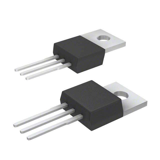
| 描述 | TRANS DARL NPN 8A 100V TO-220AB达林顿晶体管 8A 100V Bipolar Power NPN |
| 产品分类 | 晶体管(BJT) - 单路分离式半导体 |
| 品牌 | ON Semiconductor |
| 产品手册 | |
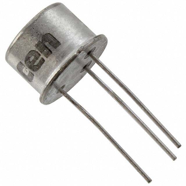
| 产品图片 |
|
| rohs | 符合RoHS无铅 / 符合限制有害物质指令(RoHS)规范要求 |
| 产品系列 | 晶体管,达林顿晶体管,ON Semiconductor BDX53CG- |
| 数据手册 | |
| 产品型号 | BDX53CG |
| 不同 Ib、Ic时的 Vce饱和值(最大值) | 2V @ 12mA,3A |
| 不同 Ic、Vce 时的DC电流增益(hFE)(最小值) | 750 @ 3A,3V |
| 产品目录页面 | |
| 产品种类 | 达林顿晶体管 |
| 供应商器件封装 | TO-220AB |
| 其它名称 | BDX53CG-ND |
| 功率-最大值 | 65W |
| 功率耗散 | 40 W |
| 包装 | 管件 |
| 发射极-基极电压VEBO | 5 V |
| 商标 | ON Semiconductor |
| 安装类型 | 通孔 |
| 安装风格 | Through Hole |
| 封装 | Tube |
| 封装/外壳 | TO-220-3 |
| 封装/箱体 | TO-220-3 |
| 工厂包装数量 | 50 |
| 晶体管极性 | NPN |
| 晶体管类型 | NPN - 达林顿 |
| 最大工作温度 | + 150 C |
| 最大直流电集电极电流 | 8 A |
| 最大集电极截止电流 | 500 uA |
| 最小工作温度 | - 65 C |
| 标准包装 | 50 |
| 电压-集射极击穿(最大值) | 100V |
| 电流-集电极(Ic)(最大值) | 8A |
| 电流-集电极截止(最大值) | 500µA |
| 直流集电极/BaseGainhfeMin | 750 |
| 系列 | BDX53C |
| 配置 | Single |
| 集电极—发射极最大电压VCEO | 100 V |
| 集电极—基极电压VCBO | 100 V |
| 集电极连续电流 | 4 A |
| 频率-跃迁 | - |


PDF Datasheet 数据手册内容提取
BDX53B, BDX53C (NPN), BDX54B, BDX54C (PNP) Plastic Medium-Power Complementary Silicon Transistors www.onsemi.com These devices are designed for general−purpose amplifier and low−speed switching applications. DARLINGTON Features 8 AMPERE • High DC Current Gain − COMPLEMENTARY SILICON h = 2500 (Typ) @ I = 4.0 Adc FE C POWER TRANSISTORS • Collector Emitter Sustaining Voltage − @ 100 mAdc 80−100 VOLTS, 65 WATTS V = 80 Vdc (Min) − BDX53B, 54B CEO(sus) V = 100 Vdc (Min) − BDX53C, 54C CEO(sus) • Low Collector−Emitter Saturation Voltage − 4 V = 2.0 Vdc (Max) @ I = 3.0 Adc CE(sat) C V = 4.0 Vdc (Max) @ I = 5.0 Adc CE(sat) C • Monolithic Construction with Built−In Base−Emitter Shunt Resistors • These Devices are Pb−Free and are RoHS Compliant* ÎÎÎÎÎÎÎÎÎÎÎÎÎÎÎÎÎÎÎ ÎÎÎÎMAÎÎXIMÎÎUMÎÎ RATÎÎINGÎÎS ÎÎÎÎÎÎÎÎÎÎÎÎÎÎÎÎÎÎÎÎÎÎÎÎÎÎÎ 1 ÎÎÎÎÎÎÎÎÎÎÎÎRatÎÎing ÎÎÎÎÎÎÎÎÎÎÎÎSymÎÎboÎÎÎÎl ÎÎVaÎÎlue ÎÎÎÎÎÎUniÎÎt 23 ÎÎColÎlectoÎr−EmÎitteÎr VolÎtageÎÎÎÎÎÎVCÎEOÎÎÎÎÎÎÎVdcÎ TO−220 BDX53B, BDX54B 80 ÎÎÎÎÎÎÎÎÎÎÎÎÎÎÎÎÎÎÎÎÎÎÎÎÎÎÎÎÎÎÎÎÎÎÎÎÎÎÎÎÎÎÎÎ CASE 221A BDX53C, BDX54C 100 STYLE 1 ÎÎColÎlectoÎr−BaÎse VÎoltaÎge ÎÎÎÎÎÎVÎCB ÎÎÎÎÎÎÎVdcÎ BDX53B, BDX54B 80 ÎÎÎÎÎÎÎÎÎÎÎÎÎÎÎÎÎÎÎÎÎÎ MARKING DIAGRAM BDX53C, BDX54C 100 ÎÎÎÎÎÎÎÎÎÎÎÎÎÎÎÎÎÎÎÎÎÎÎÎÎÎÎÎÎÎÎÎÎÎÎÎÎÎÎÎÎÎÎÎÎÎÎÎÎÎÎÎÎÎÎÎÎÎÎÎÎÎÎÎÎÎ & PIN ASSIGNMENT Emitter−Base Voltage VEB 5.0 Vdc ÎÎColÎlectoÎr CuÎrrentÎ−Î CoÎntinuÎousÎÎÎÎÎIC ÎÎÎ8Î.0 ÎÎÎAdcÎ 4 − Peak 12 Collector ÎÎÎÎÎÎÎÎÎÎÎÎÎÎÎÎÎÎÎÎÎÎÎÎÎÎÎÎÎÎÎÎÎÎÎÎÎÎÎÎÎÎÎÎ ÎÎÎÎBasÎÎe CuÎÎrrenÎÎt ÎÎÎÎÎÎÎÎÎÎÎÎÎÎÎÎÎÎIB ÎÎÎÎÎÎ0ÎÎ.2 ÎÎÎÎÎÎAdcÎÎ Total Device Dissipation @ TC = 25°C PD 65 W ÎÎÎÎDerÎÎate aÎÎbovÎÎe 25ÎΰC ÎÎÎÎÎÎÎÎÎÎÎÎÎÎÎÎÎÎÎÎÎÎ0.ÎÎ48 ÎÎÎÎÎÎW/°CÎÎ BDX5xyG ÎÎOpeÎratinÎg anÎd SÎtoragÎe JuÎnctioÎn ÎÎÎÎTJ,Î TstgÎÎ−Î65 toÎ +15ÎÎ0 ΰCÎ Temperature Range AY WW ÎÎÎÎÎÎÎÎÎÎÎÎÎÎÎÎÎÎÎÎÎÎ Stresses exceeding those listed in the Maximum Ratings table may damage the device. If any of these limits are exceeded, device functionality should not be 1 3 assumed, damage may occur and reliability may be affected. Base 2 Emitter Collector ÎÎÎÎÎÎÎÎÎÎÎÎÎÎÎÎÎÎÎ THERMAL CHARACTERISTICS BDX5xy= Device Code ÎÎÎÎÎÎÎÎÎÎÎÎÎÎÎÎÎÎÎÎÎÎÎÎÎÎÎÎÎÎÎÎÎÎÎÎÎÎÎÎÎ Characteristic Symbol Max Unit x = 3 or 4 ÎÎÎÎÎÎÎÎÎÎÎÎÎÎÎÎÎÎÎÎÎÎÎÎÎÎÎÎÎÎÎÎÎÎÎÎÎÎÎÎÎÎÎÎÎÎÎÎÎÎÎÎÎÎÎÎÎÎÎÎÎÎÎÎÎÎ y = B or C Thermal Resistance, Junction−to−Ambient R(cid:2)JA 70 °C/W A = Assembly Location ÎÎTheÎrmaÎl ResÎistanÎce, ÎJuncÎtionÎ−to−ÎCaseÎÎÎRÎ(cid:2)JCÎÎÎ1.Î92 ÎÎΰC/WÎ Y = Year WW = Work Week G = Pb−Free Package *For additional information on our Pb−Free strategy and soldering details, please ORDERING INFORMATION download the ON Semiconductor Soldering and Mounting Techniques See detailed ordering and shipping information in the package Reference Manual, SOLDERRM/D. dimensions section on page 6 of this data sheet. © Semiconductor Components Industries, LLC, 2014 1 Publication Order Number: November, 2014 − Rev. 15 BDX53B/D
BDX53B, BDX53C (NPN), BDX54B, BDX54C (PNP) TA TC 4.0 80 S) T T A 3.0 60 W N ( TIO TC A P SI 2.0 40 S DI R WE TA O 1.0 20 P , D P 0 0 20 40 60 80 100 120 140 160 T, TEMPERATURE (°C) Figure 1. Power Derating ELECTRICAL CHARACTERISTICS (TC = 25°C unless otherwise noted) Characteristic Symbol Min Max Unit OFF CHARACTERISTICS Collector−Emitter Sustaining Voltage (Note 1) VCEO(sus) Vdc (IC = 100 mAdc, IB = 0) BDX53B, BDX54B 80 − BDX53C, BDX54C 100 − Collector Cutoff Current ICEO mAdc (VCE = 40 Vdc, IB = 0) BDX53B, BDX54B − 0.5 (VCE = 50 Vdc, IB = 0) BDX53C, BDX54C − 0.5 Collector Cutoff Current ICBO mAdc (VCB = 80 Vdc, IE = 0) BDX53B, BDX54B − 0.2 (VCB = 100 Vdc, IE = 0) BDX53C, BDX54C − 0.2 ON CHARACTERISTICS (Note 1) DC Current Gain hFE 750 − − (IC = 3.0 Adc, VCE = 3.0 Vdc) Collector−Emitter Saturation Voltage VCE(sat) − 2.0 Vdc (IC = 3.0 Adc, IB = 12 mAdc) − 4.0 Base−Emitter Saturation Voltage VBE(sat) − 2.5 Vdc (IC = 3.0 Adc, IC = 12 mA) DYNAMIC CHARACTERISTICS Small−Signal Current Gain hfe 4.0 − − (IC = 3.0 Adc, VCE = 4.0 Vdc, f = 1.0 MHz) Output Capacitance Cob pF (VCB = 10 Vdc, IE = 0, f = 0.1 MHz) BDX53B, 53C − 300 BDX54B, 54C − 200 Product parametric performance is indicated in the Electrical Characteristics for the listed test conditions, unless otherwise noted. Product performance may not be indicated by the Electrical Characteristics if operated under different conditions. 1. Pulse Test: Pulse Width ≤ 300 (cid:3)s, Duty Cycle ≤ 2%. www.onsemi.com 2
BDX53B, BDX53C (NPN), BDX54B, BDX54C (PNP) VCC 5.0 RB ANDD R1C M VUASRTIE BDE TFOA SOTB RTAEICNO DVEESRIRY ETDY PCEUSR,R eE.gN.:T LEVELS -30 V 3.0 ts (cid:4)(cid:4)1MNS5D862150 U0 SUESDE DA BBOEVLEO WIB (cid:3)IB (cid:3) 10 100 m0A mA RCSCOPE 2.0 TUT 1.0 tf V2 RB μ(cid:2)(cid:3)s) 0.7 APPROX ME ( 0.5 +8.00 V 51 D1 (cid:3) 8.0 k (cid:3) 120 t, TI 0.3 tr V1 +4.0 V 0.2 VCC = 30 V A-P1P2R OVX 25 (cid:3)s for td and tr, D1 is disconnected 0.1 IICB1/I B= =IB 2250 tDr,U tfT (cid:2)Y C 1Y0C nLsE = 1.0% aFnodr NVP2 N= t0est circuit reverse all polarities 00..00570.1 TJ = 205.°2C 0.3 0.5 td0 .@7 VB1E.0(off) = 0 V2.0 3.0 5.0 7.0 10 IC, COLLECTOR CURRENT (AMP) Figure 2. Switching Time Test Circuit Figure 3. Switching Times 1.0 ED) 0.7 D = 0.5 Z TLI 0.5 NA EM NSIOR 0.3 0.2 r(t) EFFECTIVE TRATHERMAL RESISTANCE (N000000....0000..217532 000...001052.01 SINGLE PULSE P(pk)DUTtY1 CtY2CLE, DS P=IU Nt1LG/StL2EE RRTDPRJU E(cid:2)(cid:2)C(JJpLACCUkSD)( R=tE- )T V 1=TTIEM. CR9rS( E2At= )°A I ACNPRPT/( (cid:2)PpWS JtkL1HC)Y OR F(cid:2)WOJCNR(t )POWER 0.01 0.01 0.020.03 0.05 0.1 0.2 0.3 0.5 1.0 2.0 3.0 5.0 10 20 30 50 100 200 300 500 1000 t, TIME OR PULSE WIDTH (ms) Figure 4. Thermal Response 20 There are two limitations on the power handling ability of 100 (cid:3)s 10 500 (cid:3)s a transistor average junction temperature and second P) AM 5.0 breakdown. Safe operating area curves indicate IC −VCE T ( 5.0 ms limits of the transistor that must be observed for reliable RREN 2.0 TJ = 150°C 1.0 ms dc operation, i.e., the transistor must not be subjected to greater U 1.0 BONDING WIRE LIMITED dissipation than the curves indicate. C OR 0.5 THERMALLY LIMITED @ TC = 25°C The data of Figure 5 is based on TJ(pk) = 150°C; TC is CT (cid:4)(SINGLE PULSE) variable depending on conditions. Second breakdown pulse LLE 0.2 SECOND BREAKDOWN LIMITED limits are valid for duty cycles to 10% provided , COC0.1 CURVES APPLY BELOW RATED VCEO TJ(pk) (cid:4) 150°C. TJ(pk) may be calculated from the data in I Figure 4. At high case temperatures, thermal limitations will 0.05 BDX53B, BDX54B reduce the power that can be handled to values less than the BDX53C, BDX54C 0.02 limitations imposed by second breakdown. 1.0 2.0 3.0 5.0 7.0 10 20 30 50 70 100 VCE, COLLECTOR-EMITTER VOLTAGE (VOLTS) Figure 5. Active−Region Safe Operating Area www.onsemi.com 3
BDX53B, BDX53C (NPN), BDX54B, BDX54C (PNP) 10,000 300 N 5000 TJ = + 25°C AI G 3000 200 T 2000 N RE 1000 pF) UR E ( LL-SIGNAL C 531200000000 TVICJC =E= 3=2. 503° .AC0 V CAPACITANC 17000 Cib Cob MA C, , SFE 3500 PNP 50 PNP h 20 NPN NPN 10 30 1.0 2.0 5.0 10 20 50 100 200 500 1000 0.1 0.2 0.5 1.0 2.0 5.0 10 20 50 100 f, FREQUENCY (kHz) VR, REVERSE VOLTAGE (VOLTS) Figure 6. Small-Signal Current Gain Figure 7. Capacitance NPN PNP BDX53B, 53C BDX54B, 54C 20,000 20,000 VCE = 4.0 V VCE = 4.0 V 10,000 10,000 N N T GAI 5000 TJ = 150°C T GAI 5000 TJ = 150°C EN 3000 EN 3000 R R CUR 2000 25°C CUR 2000 25°C C C D 1000 D 1000 h, FE -(cid:5)55°C h, FE -(cid:5)55°C 500 500 300 300 200 200 0.1 0.2 0.3 0.5 0.7 1.0 2.0 3.0 5.0 7.0 10 0.1 0.2 0.3 0.5 0.7 1.0 2.0 3.0 5.0 7.0 10 IC, COLLECTOR CURRENT (AMP) IC, COLLECTOR CURRENT (AMP) Figure 8. DC Current Gain S) 3.0 S) 3.0 T T OL TJ = 25°C OL TJ = 25°C V V GE ( 2.6 GE ( 2.6 A A LT IC = 2.0 A 4.0 A 6.0 A LT IC = 2.0 A 4.0 A 6.0 A O O V V R 2.2 R 2.2 E E T T T T MI MI E E - 1.8 - 1.8 R R O O T T C C E E LL 1.4 LL 1.4 O O C C , E , E C C V 1.0 V 1.0 0.3 0.5 0.7 1.0 2.0 3.0 5.0 7.0 10 20 30 0.3 0.5 0.7 1.0 2.0 3.0 5.0 7.0 10 20 30 IB, BASE CURRENT (mA) IB, BASE CURRENT (mA) Figure 9. Collector Saturation Region www.onsemi.com 4
BDX53B, BDX53C (NPN), BDX54B, BDX54C (PNP) 3.0 3.0 TJ = 25°C TJ = 25°C 2.5 2.5 S) S) T T L L O O V V E ( 2.0 E ( 2.0 G G A A T T L L V, VO 1.5 VBE(sat) @ IC/IB = 250 V, VO 1.5 VBE @ VCE = 4.0 V 1.0 VBE @ VCE = 4.0 V 1.0 VBE(sat) @ IC/IB = 250 VCE(sat) @ IC/IB = 250 VCE(sat) @ IC/IB = 250 0.5 0.5 0.1 0.2 0.3 0.5 0.7 1.0 2.0 3.0 5.0 7.0 10 0.1 0.2 0.3 0.5 0.7 1.0 2.0 3.0 5.0 7.0 10 IC, COLLECTOR CURRENT (AMP) IC, COLLECTOR CURRENT (AMP) Figure 10. “On” Voltages NPN PNP BDX53B, BDX53C BDX54B, BDX54C +(cid:5)5.0 +(cid:5)5.0 C) C) ° +(cid:5)4.0 ° +(cid:5)4.0 mV/ *IC/IB (cid:2) hFE/3 mV/ *IC/IB (cid:2) hFE/3 T ( +(cid:5)3.0 T ( +(cid:5)3.0 EN +(cid:5)2.0 25°C to 150°C EN +(cid:5)2.0 25°C to 150°C CI CI FFI +(cid:5)1.0 FFI +(cid:5)1.0 OE -(cid:5)55°C to 25°C OE -(cid:5)55°C to 25°C C 0 C 0 E E UR -(cid:5)1.0 *(cid:2)VC for VCE(sat) UR -(cid:5)1.0 *(cid:2)VC for VCE(sat) T T A A R -(cid:5)2.0 R -(cid:5)2.0 PE 25°C to 150°C PE 25°C to 150°C , TEMV--(cid:5)(cid:5)43..00 (cid:2)VB for VBE -(cid:5)55 to 150°C , TEMV--(cid:5)(cid:5)43..00 (cid:2)VB for VBE -(cid:5)55 to 150°C θ θ -(cid:5)5.0 -(cid:5)5.0 0.1 0.2 0.3 0.5 0.7 1.0 2.0 3.0 5.0 7.0 10 0.1 0.2 0.3 0.5 0.7 1.0 2.0 3.0 5.0 7.0 10 IC, COLLECTOR CURRENT (AMP) IC, COLLECTOR CURRENT (AMP) Figure 11. Temperature Coefficients 105 105 REVERSE FORWARD REVERSE FORWARD μ, COLLECTOR CURRENT ((cid:2)(cid:3)A)IC 111110000021034 TJ = V115C000E°° =CC 30 V μ, COLLECTOR CURRENT ((cid:2)(cid:3)A)IC 111110000021034 TVJ C=E 11 =502 0053°°°0CCC V 25°C 10-(cid:5)1 10-(cid:5)1 -(cid:5)0.6 -(cid:5)0.4 -(cid:5)0.2 0 +(cid:5)0.2 +(cid:5)0.4 +(cid:5)0.6 +(cid:5)0.8 +(cid:5)1.0 +(cid:5)1.2 + 1.4 +(cid:5)0.6 +(cid:5)0.4 +(cid:5)0.2 0 -(cid:5)0.2 -(cid:5)0.4 -(cid:5)0.6 -(cid:5)0.8 -(cid:5)1.0 -(cid:5)1.2 -(cid:5)1.4 VBE, BASE‐EMITTER VOLTAGE (VOLTS) VBE, BASE‐EMITTER VOLTAGE (VOLTS) Figure 12. Collector Cut−Off Region www.onsemi.com 5
BDX53B, BDX53C (NPN), BDX54B, BDX54C (PNP) NPN COLLECTOR PNP COLLECTOR BDX53B BDX54B BDX53C BDX54C BASE BASE (cid:3) 8.0 k (cid:3) 120 (cid:3) 8.0 k (cid:3) 120 EMITTER EMITTER Figure 13. Darlington Schematic ORDERING INFORMATION Device Package Shipping† BDX53BG TO−220 50 Units / Rail (Pb−Free) BDX53CG TO−220 50 Units / Rail (Pb−Free) BDX54BG TO−220 50 Units / Rail (Pb−Free) BDX54CG TO−220 50 Units / Rail (Pb−Free) †For information on tape and reel specifications, including part orientation and tape sizes, please refer to our Tape and Reel Packaging Specifications Brochure, BRD8011/D. www.onsemi.com 6
BDX53B, BDX53C (NPN), BDX54B, BDX54C (PNP) PACKAGE DIMENSIONS TO−220 CASE 221A−09 ISSUE AH NOTES: 1. DIMENSIONING AND TOLERANCING PER ANSI Y14.5M, 1982. −T− SPELAATNIENG 2. CONTROLLING DIMENSION: INCH. 3. DIMENSION Z DEFINES A ZONE WHERE ALL B F C BODY AND LEAD IRREGULARITIES ARE T S ALLOWED. INCHES MILLIMETERS 4 DIM MIN MAX MIN MAX A 0.570 0.620 14.48 15.75 Q A B 0.380 0.415 9.66 10.53 C 0.160 0.190 4.07 4.83 1 2 3 U D 0.025 0.038 0.64 0.96 F 0.142 0.161 3.61 4.09 H G 0.095 0.105 2.42 2.66 H 0.110 0.161 2.80 4.10 K J 0.014 0.024 0.36 0.61 Z K 0.500 0.562 12.70 14.27 L 0.045 0.060 1.15 1.52 N 0.190 0.210 4.83 5.33 L R Q 0.100 0.120 2.54 3.04 R 0.080 0.110 2.04 2.79 V J S 0.045 0.055 1.15 1.39 T 0.235 0.255 5.97 6.47 G U 0.000 0.050 0.00 1.27 D V 0.045 --- 1.15 --- Z --- 0.080 --- 2.04 N STYLE 1: PIN 1. BASE 2. COLLECTOR 3. EMITTER 4. COLLECTOR ON Semiconductor and the are registered trademarks of Semiconductor Components Industries, LLC (SCILLC) or its subsidiaries in the United States and/or other countries. SCILLC owns the rights to a number of patents, trademarks, copyrights, trade secrets, and other intellectual property. A listing of SCILLC’s product/patent coverage may be accessed at www.onsemi.com/site/pdf/Patent−Marking.pdf. SCILLC reserves the right to make changes without further notice to any products herein. SCILLC makes no warranty, representation or guarantee regarding the suitability of its products for any particular purpose, nor does SCILLC assume any liability arising out of the application or use of any product or circuit, and specifically disclaims any and all liability, including without limitation special, consequential or incidental damages. “Typical” parameters which may be provided in SCILLC data sheets and/or specifications can and do vary in different applications and actual performance may vary over time. All operating parameters, including “Typicals” must be validated for each customer application by customer’s technical experts. SCILLC does not convey any license under its patent rights nor the rights of others. SCILLC products are not designed, intended, or authorized for use as components in systems intended for surgical implant into the body, or other applications intended to support or sustain life, or for any other application in which the failure of the SCILLC product could create a situation where personal injury or death may occur. Should Buyer purchase or use SCILLC products for any such unintended or unauthorized application, Buyer shall indemnify and hold SCILLC and its officers, employees, subsidiaries, affiliates, and distributors harmless against all claims, costs, damages, and expenses, and reasonable attorney fees arising out of, directly or indirectly, any claim of personal injury or death associated with such unintended or unauthorized use, even if such claim alleges that SCILLC was negligent regarding the design or manufacture of the part. SCILLC is an Equal Opportunity/Affirmative Action Employer. This literature is subject to all applicable copyright laws and is not for resale in any manner. PUBLICATION ORDERING INFORMATION LITERATURE FULFILLMENT: N. American Technical Support: 800−282−9855 Toll Free ON Semiconductor Website: www.onsemi.com Literature Distribution Center for ON Semiconductor USA/Canada P.O. Box 5163, Denver, Colorado 80217 USA Europe, Middle East and Africa Technical Support: Order Literature: http://www.onsemi.com/orderlit Phone: 303−675−2175 or 800−344−3860 Toll Free USA/Canada Phone: 421 33 790 2910 Fax: 303−675−2176 or 800−344−3867 Toll Free USA/Canada Japan Customer Focus Center For additional information, please contact your local Email: orderlit@onsemi.com Phone: 81−3−5817−1050 Sales Representative www.onsemi.com BDX53B/D 7
Mouser Electronics Authorized Distributor Click to View Pricing, Inventory, Delivery & Lifecycle Information: O N Semiconductor: BDX53BG BDX53CG BDX54BG BDX54CG