ICGOO在线商城 > BD9845FV-E2
 Datasheet下载
- 型号: BD9845FV-E2
- 制造商: ROHM Semiconductor
- 库位|库存: xxxx|xxxx
- 要求:
| 数量阶梯 | 香港交货 | 国内含税 |
| +xxxx | $xxxx | ¥xxxx |
查看当月历史价格
查看今年历史价格
BD9845FV-E2产品简介:
ICGOO电子元器件商城为您提供BD9845FV-E2由ROHM Semiconductor设计生产,在icgoo商城现货销售,并且可以通过原厂、代理商等渠道进行代购。 提供BD9845FV-E2价格参考¥5.06-¥9.80以及ROHM SemiconductorBD9845FV-E2封装/规格参数等产品信息。 你可以下载BD9845FV-E2参考资料、Datasheet数据手册功能说明书, 资料中有BD9845FV-E2详细功能的应用电路图电压和使用方法及教程。
| 参数 | 数值 |
| 产品目录 | 集成电路 (IC) |
| Cuk | 无 |
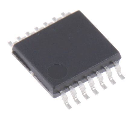
| 描述 | IC REG CTRLR BUCK PWM 14-SSOP |
| 产品分类 | |
| 品牌 | Rohm Semiconductor |
| 数据手册 | |
| 产品图片 |
|
| 产品型号 | BD9845FV-E2 |
| PWM类型 | 控制器 |
| rohs | 无铅 / 符合限制有害物质指令(RoHS)规范要求 |
| 产品系列 | - |
| 产品目录页面 | |
| 倍增器 | 无 |
| 其它名称 | BD9845FV-E2DKR |
| 分频器 | 无 |
| 包装 | Digi-Reel® |
| 升压 | 无 |
| 占空比 | 100% |
| 反向 | 无 |
| 反激式 | 无 |
| 封装/外壳 | 14-LSSOP(0.173",4.40mm 宽) |
| 工作温度 | -40°C ~ 85°C |
| 标准包装 | 1 |
| 电压-电源 | 3.6 V ~ 35 V |
| 输出数 | 1 |
| 降压 | 是 |
| 隔离式 | 无 |
| 频率-最大值 | 1.5MHz |


- 商务部:美国ITC正式对集成电路等产品启动337调查
- 曝三星4nm工艺存在良率问题 高通将骁龙8 Gen1或转产台积电
- 太阳诱电将投资9.5亿元在常州建新厂生产MLCC 预计2023年完工
- 英特尔发布欧洲新工厂建设计划 深化IDM 2.0 战略
- 台积电先进制程称霸业界 有大客户加持明年业绩稳了
- 达到5530亿美元!SIA预计今年全球半导体销售额将创下新高
- 英特尔拟将自动驾驶子公司Mobileye上市 估值或超500亿美元
- 三星加码芯片和SET,合并消费电子和移动部门,撤换高东真等 CEO
- 三星电子宣布重大人事变动 还合并消费电子和移动部门
- 海关总署:前11个月进口集成电路产品价值2.52万亿元 增长14.8%


PDF Datasheet 数据手册内容提取
DDaattaasshheeeett 3.6V to 35V Input 1ch Buck Controller BD9845FV General Description Key Specifications BD9845FV is a switching regulator controller that uses Supply Voltage Range: 3.6V to 35V pulse width modulation. This IC can be used for Error Amplifier Reference Voltage: 1.0V±1% step-down DC/DC converter applications. BD9845FV is Oscillation Frequency: 100kHz to 1500kHz available in a compact package that is optimum for Standby Current: 0µA(Typ) compact power supplies of many kinds of equipment. Operating Temperature Range: -40°C to +85°C Features Package W(Typ) x D(Typ) x H(Max) Operates up to (VCC=35V) Contains FET Driver Circuit (Step-Down Circuit 1 output). REG Output Circuit (2.5V) are contained. Built-In Over Current Protect Adjustable Soft Start and Pause Period. Three modes of Standby, Master, and Slave can be Switched. (ICCS = 0 µA typ during standby) ON/OFF control is enabled independently for each channel. (DT terminal) Applications SSOP-B14 LCD, PDP, PC, AV, Printer, DVD, Projector TV, Fax, 5.00mm x 6.40mm x 1.35mm Copy Machine, Measuring Instrument, etc Typical Application Circuit VIN VCC STB VCC VREF VREF VCC VREF VCC- 5VREG 5V C5V CT OSC UVLO TSD INV VREF VCC SS +-ERR +-PWM DRV OUT (Step-dVoOwn) + + VCC VCC FB OCP2OCP- -5V + DT VCC- 5V OCP+ OCP- GND Figure 1. Typical Application Circuit ○Product structure:Silicon monolithic integrated circuit ○This product has no designed protection against radioactive rays www.rohm.com TSZ02201-0Q3Q0AJ00470-1-2 © 2015 ROHM Co., Ltd. All rights reserved. 1/25 TSZ22111・14・001 06.Nov.2015 Rev.001
BD9845FV Pin Configuration (TOP VIEW) 1 VREF DT 14 2 CT SS 1 3 3 GND INV 12 4 STB FB 1 1 5 C5V SEL 10 6 OUT OCP- 9 7 VCC OCP+ 8 Pin Description Pin Pin Pin Pin Function Function Number Name Number Name Reference voltage (2.5V) Output over-current detector 1 VREF 8 OCP+ output terminal + input terminal Output over-current detector 2 CT Timing capacity external terminal 9 OCP- - input terminal 3 GND Ground 10 SEL Master/Slave mode setting terminal 4 STB Standby mode setting terminal 11 FB Output error amplifier output terminal 5 C5V Output L side voltage (VCC-5V) 12 INV Output error amplifier - input terminal 6 OUT Output 13 SS Output soft start time setting terminal 7 VCC Power terminal 14 DT Output dead time setting terminal Block Diagram VCC STB SEL OCP+ OCP- VCC VCC VREF + VCC REG STB MASTER - OCP + REG VREF (2.5V) /SLAVE OCP- C5V (VCC-5V) 50mV±10mV C5V C5V DT - DTLow DTOFF DT FB + 1.25V VREF 1V±10mV VCC 2μA + + SS + ERR + PWM LS DRV OUT SSOFF - - C5V INV PROTECTION LOGIC OSC DTLow SSOFF 200μA TSD OCP TSD 200μ--+A 1.5V 2.0V (H1o.6ldm tsiemce) DTOFF UVLO TSD Hold time VCC 3.2V (0.2msec) M/SALSATVEER 2V VREF 2.2V UVLO UVLO CT 1.5V C5V 3V GND www.rohm.com TSZ02201-0Q3Q0AJ00470-1-2 © 2015 ROHM Co., Ltd. All rights reserved. 2/25 TSZ22111・15・001 06.Nov.2015 Rev.001
BD9845FV Absolute Maximum Ratings Item Symbol Rating Unit Supply Voltage VCC 36 V Permissible Loss Pd 0.50 (Note 1) W OUT Terminal Voltage VOUT VCC-7V to VCC V C5V Terminal Voltage VC5V VCC-7V to VCC V OCP Terminal Voltage VOCP VCC-7V to VCC V Operation Temperature Range Topr -40 to +85 °C Storage Temperature Range Tstg -55 to +150 °C Joint Temperature Tjmax 150 °C (Note 1) When mounted on a 70.0 mm 70.0 mm 1.6 mm glass epoxy board. Derate by 4.0 mW/C above Ta=25C. Caution: Operating the IC over the absolute maximum ratings may damage the IC. In addition, it is impossible to predict all destructive situations such as short-circuit modes, open circuit modes, etc. Therefore, it is important to consider circuit protection measures, like adding a fuse, in case the IC is operated in a special mode exceeding the absolute maximum ratings. Recommended Operating Conditions (Ta=25C) Item Symbol Range Unit Supply Voltage VCC 3.6 to 35 V Output Terminal Voltage VOUT VC5V to VCC V Timing Capacity CCT 47 to 3000 pF Error Amplifier Input Voltage VINV 0 to VREF-0.9 V DT Terminal Input Voltage VDT 0 to VREF V OCP+/- Input Voltage VOCP VCC±0.2 V Oscillation Frequency fOSC 100 to 1500 kHz STB Input Voltage VSTB 0 to VCC V SEL Input Voltage VSEL 0 to VCC V www.rohm.com TSZ02201-0Q3Q0AJ00470-1-2 © 2015 ROHM Co., Ltd. All rights reserved. 3/25 TSZ22111・15・001 06.Nov.2015 Rev.001
BD9845FV Electrical Characteristics (Unless otherwise specified, Ta=25C, VCC=6V) Standard Value Item Symbol Unit Conditions Min Typ Max [VREF Output Unit] Output Voltage VREF 2.450 2.500 2.550 V IOUT= 0.1mA Input Stability(Line Reg.) VLI_REG - 1 10 mV VCC= 3.6V to 35V Load Stability(Load Reg.) VLO_REG - 2 10 mV IOUT= 0.1mA to 2mA Current Capacity IOMAX 2 13 - mA VREF= (Typ)x0.95 [Triangular Wave Oscillator] Oscillation Frequency fOSC 95 106 117 kHz CCP= 1800pF Frequency Fluctuation fDV - 0 1 % VCC= 3.6V to 35V [Soft Start Unit] SS Source Current ISSSO 1.4 2 2.6 µA VSS= 0.5V SS Sink Current ISSSI 5 12 - mA VSS= 0.5V [Pause Period Adjusting Circuit] DT Input Bias Current IDT - 0.1 1 µA VDT= 1.75V DT Sink Current IDTSI 1 3.3 - mA VDT= 1.75V, (VOCP+)-(VOCP-)= 0.5V [Low Input Malfunction Preventing Circuit] Threshold Voltage VUTH 3.0 3.2 3.4 V VCC Start Detection Hysteresis VUHYS - 0.15 0.25 V [Error Amplifier] Non-Inverting Input Reference Voltage VINV 0.99 1 1.01 V INV= FB Reference Voltage Supply Fluctuation dVINV - 1 6 mV VCC= 3.6V to 35V INV Input Bias Current IIB - 0 1 µA VINV= 1V Open Gain AV 65 85 - dB Max Output Voltage VFBH 2.30 - VREF V Min Output Voltage VFBL - 0.6 1.3 V Output Sink Current IFBSI 0.5 1.5 - mA VFB= 1.25V, VINV= 1.5V Output Source Current IFBSO 50 105 - µA VFB= 1.25V, VINV= 0.5V [PWM Comparator] Input Threshold Voltage (fOSC=100kHz) Vth0 1.4 1.5 1.6 V On Duty 0% Vth100 1.9 2 2.1 V On Duty 100% [Output Unit] Output ON Resistance H RONH - 4.0 10 Ω RONH= (VCC -VOUT)/ IOUT, IOUT= 0.1A Output ON Resistance L RONL - 3.3 10 Ω RONL= (VOUT -VC5V)/ IOUT, IOUT= 0.1A C5V Clamp Voltage VCLMP 4.5 5 5.5 V VCLMP= VCC- VC5V , VCC > 7 V [Over-Current Protection Circuit] Over-Current Detection Threshold Voltage VOCPTH 0.04 0.05 0.06 V Voltage Between(OCP+) and (OCP-) OCP-Input Bias Current IOCP- - 0.1 10 µA OCP+= VCC, OCP-= VCC-0.5V Over-Current Detection Delay Time tDOCPTH - 200 400 ns OCP-= VCC→VCC-0.2 V Over-Current Detection Minimum Retention Time tDOCPRE 0.8 1.6 - ms OCP-= VCC-0.2V→VCC [Standby Changeover Unit] STB Flow-In Current ISTB - 55 100 µA VSTB= 6V Standby Mode Setting Range VSTBL 0 - 0.5 V Active (Master) Mode Setting Range VSTBH 3.0 - VCC V SEL Flow-in Current ISEL - 15 30 µA VSEL= 2.5V Master Mode Setting Range VSELL 0 - 0.5 V Slave Mode Setting Range VSELH 2.0 - VCC V [Device Overall] Standby Current ICCS - 0 1 µA VSTB= 0V Average Power Consumption ICCA 1 2.4 4 mA VINV= 0V, FB= H, VDT= 1.75V www.rohm.com TSZ02201-0Q3Q0AJ00470-1-2 © 2015 ROHM Co., Ltd. All rights reserved. 4/25 TSZ22111・15・001 06.Nov.2015 Rev.001
BD9845FV Typical Performance Curves 10 8 9 µA) 8 A) 7 (S 7 m 6 C ( urrent : IC 456 rent : ICCA 345 Ta=25°C Standby C 0123 VCC =6 V Circuit Cur 012 -5 0 -2 5 0 25 50 75 100 125 0 5 10 15 20 25 30 35 40 Ambient Temperature : Ta (°C) Supply Voltage : V (V) CC Figure 2. Standby Current vs Ambient Temperature Figure 3. Circuit Current vs Supply Voltage 8 2.520 A) 7 V) 2.515 urrent : I(m CCA 3456 VCC=6V Voltage: V(REF 2222....455590015050 Ta=25°C uit C 2 nce 2.490 c e Cir 1 er 2.485 ef 0 R 2.480 -5 0 -2 5 0 25 50 75 100 125 0 5 10 15 20 25 30 35 40 Ambient Temperature : Ta (°C) Supply Voltage: VCC (V) Figure 4. Circuit Current vs Ambient Temperature Figure 5. Reference Voltage vs Supply Voltage www.rohm.com TSZ02201-0Q3Q0AJ00470-1-2 © 2015 ROHM Co., Ltd. All rights reserved. 5/25 TSZ22111・15・001 06.Nov.2015 Rev.001
BD9845FV Typical Performance Curves – continued e : V(V)REF 2222....555501125050 Ta=25°C age : V (V)REF 2222....555501125050 VCC=6V ce Voltag 22..459050 V C C =6V utput Volt 22..459050 ren 2.490 e O 2.490 efe 2.485 nc 2.485 R e 2.480 0 0.5 1 1.5 2 2.5 3 3.5 4 4 .5 5 Refer 2 .(V)480- 5 0 -2 5 0 25 50 75 100 125 Reference Outpu t Current : IREF (mA) Ambient Temperature : Ta (°C) Figure 6. Reference Voltage vs Reference Output Current Figure 7. Reference Output Voltage vs Ambient Temperature (VREF Current Capability) (VREF Temperature Characteristics) 3.5 V(V)UTH 333...234 d [dB] Gain Phase d : 3.1 ose Phase ol 3 Cl esh 2.9 n : Thr 2.8 Gai O 2.7 p Gain UVL 2.6 Loo 2.5 - 50 - 25 0 25 50 75 100 125 100 1K 10K 100K 1M 10M Ambient Temperature : Ta (°C) Figure 9. Loop Gain vs Frequency Figure 8. UVLO Threshold vs Ambient Temperature (Error Amplifier I/O Characteristics) www.rohm.com TSZ02201-0Q3Q0AJ00470-1-2 © 2015 ROHM Co., Ltd. All rights reserved. 6/25 TSZ22111・15・001 06.Nov.2015 Rev.001
BD9845FV Typical Performance Curves – continued µA) 12..80 (V)NV 11.0.0018 ent : I(IB 111...246 age : VI 111...000000246 VCC=6V Curr 1.0 Volt 1 ut 0.8 ce 0.998 ErrAmp Inp 0000....0246 TVTVaaCC==CC==226655VV℃°C mp Referen 000...999999246 0.99 0 0.2 0.4 0.6 0.8 1 1.2 1.4 1.6 1.8 2 ErrA -50 -25 0 25 50 75 100 125 ErrAmp Input Voltage: VINV (V) Ambient Temperature : Ta (°C) Figure 10. Error Amplifier Input Current vs Error Figure 11. Error Amplifier Reference Voltage vs Ambient Amplifier Input Voltage Temperature A) 140 3.0 e Current : I(µFBSO 1168020000 Ta=T8a5=°- C4 0 °CT a= 25°C Current : I(mA)FBSI 1122....0505 Ta=- T4 a0=°2C5 T°aC = 8 5°C FB Sourc 24000 VCC =6 .0V FB Sink -0 00...505 VCC=6.0V 0 1 2 3 4 0 0.5 1 1.5 2 ErrAmp Output Voltage : VFB (V) ErrAmp Output Voltage : VFB (V) Figure 12. FB Source Current vs Error Amplifier Output Voltage Figure 13. FB Sink Current vs Error Amplifier Output Voltage www.rohm.com TSZ02201-0Q3Q0AJ00470-1-2 © 2015 ROHM Co., Ltd. All rights reserved. 7/25 TSZ22111・15・001 06.Nov.2015 Rev.001
BD9845FV Typical Performance Curves – continued 35 4.0 A) Ta=-40°C (µSSso 33..05 mA) 2350 Ta=25°C urce Current : I 1122....0505 VCC=6.0V Current : I(SSsi 112050 Ta=85°C VVCCCC =6.0V o k SS S 00..05 SS Sin 05 0 0.2 0.4 0.6 0.8 1 1.2 1.4 1.6 0 0.5 1 1.5 2 SS Voltage : VSS (V) SS Voltage : VSS (V) Figure 14. Soft Start Source Current vs Soft Start Voltage Figure 15. Soft Start Sink Current vs Soft Start Voltage 5 120 A) µ CCP=1800pF o ( 4 Ss z) 110 S H Current : I 23 VCC=6.0V y : f (kOSC 100 VCC=6V urce 1 uenc 90 o q S e SS 0 Fr 80 -50 -25 0 25 50 75 100 125 -50 -25 0 25 50 75 100 125 Ambient Temperature : Ta (°C) Ambient Temperature : Ta (°C) Figure 16. Soft Start Source Current vs Ambient Temperature Figure 17. Oscillation Frequency vs Ambient Temperature www.rohm.com TSZ02201-0Q3Q0AJ00470-1-2 © 2015 ROHM Co., Ltd. All rights reserved. 8/25 TSZ22111・15・001 06.Nov.2015 Rev.001
BD9845FV Typical Performance Curves – continued A) 67 mA) 67 nt : I(µDT 45 ent : I(DT 45 Ta=25T°aC= -40°C urre 3 Curr 3 Ta=85°C T Input C 12 TVaC=C=256°.0C V DT SInk 12 VCC=6.0V D 0 0 0 0.5 1 1.5 2 2.5 0 0.5 1 1.5 2 2.5 DT Input Voltage : VDT (V) DT Input Voltage : V (V) DT Figure 18. DT Input Bias Current vs DT Input Voltage Figure 19. DT Sink Current vs DT Input Voltage %)100 %)100 ( Output Duty Cycle : Duty 1234567890000000000 VTaCC==265.°0CV utput Duty Cycle : Duty ( 1234567890000000000 VTaCC==265.°0CV O 1.4 1.6 1.8 2 2.2 1.4 1.6 1.8 2 2.2 DT Input Voltage : V (V) DT Input Voltage : V (V) DT DT Figure 20. Output Duty Cycle vs DT Input Voltage Figure 21. Output Duty Cycle vs DT Input Voltage (100kHz) (1.5MHz) www.rohm.com TSZ02201-0Q3Q0AJ00470-1-2 © 2015 ROHM Co., Ltd. All rights reserved. 9/25 TSZ22111・15・001 06.Nov.2015 Rev.001
BD9845FV Typical Performance Curves - continued 40 40 35 Ta=-40°C 35 Ta=-40°C 30 Ta=25°C 30 Ta=25°C mA) 25 Ta=85°C mA) 25 Ta=85°C (DS 20 VTaC=C=265.°0CV I(DS 20 I 15 15 10 10 VCC=6.0V 5 5 0VCC V-0C.C0 5 V-0CC.1 0 V-0CC.1 5 V-0CC.2 0 0C5V C-05.0V5 C-05.V1 0 C-05.1V5 C-05.V20 Output Voltage :VOUT (V) Output Voltage : VOUT (V) Figure 22. IDS vs Output Voltage Figure 23. IDS vs Output Voltage (Output ON Resistance H (RONH)) (Output ON Resistance L (RONL)) 70 500 µA) 440500 VTCaC==8355°VC mV) 6605 Flow-In Current: I(STB 122335050500000 Ta=-4T0a°C=2 5°C hreshold : V(OCPTH 44550505 VCC=6V TB 100 P T 35 S 50 OC 30 -50 -25 0 25 50 75 100 125 0 0 5 10 15 20 25 30 35 40 Ambient Temperature : Ta (°C) STB Input Voltage: V (V) STB Figure 24. STB Flow-In Current vs STB Input Voltage Figure 25. Over-Current Detection Threshold Voltage vs Ambient Temperature www.rohm.com TSZ02201-0Q3Q0AJ00470-1-2 © 2015 ROHM Co., Ltd. All rights reserved. 10/25 TSZ22111・15・001 06.Nov.2015 Rev.001
BD9845FV Typical Performance Curves - continued 5.0 5.5 4.5 5.4 V) 334...050 VTaC=C=255.°0CV (V)5V 555...123 VTaC=C=265.°0CV V(C5V 2.5 -VC 5.0 2.0 C 4.9 C 1.5 V 4.8 1.0 4.7 0.5 4.6 0.0 4.5 0 50 100 150 200 250 0 5 10 15 20 25 30 35 40 IC5V(mA) IC5V (mA) Figure 26. C5V Saturation Voltage Figure 27. C5V Load Regulation 10 9 8 7 ) V 6 (V C5 5 V -CC 4 V 3 Ta=25°C 2 1 0 0 5 10 15 20 25 30 35 40 Supply Voltage : V (V) CC Figure 28. C5V Line Regulation www.rohm.com TSZ02201-0Q3Q0AJ00470-1-2 © 2015 ROHM Co., Ltd. All rights reserved. 11/25 TSZ22111・15・001 06.Nov.2015 Rev.001
BD9845FV Application Information 1. Operation Description of Each Block and Function (1) REG: Reference Voltage Unit The REG (2.5V) produces a voltage of 2.5V which is more stable than the supply voltage input to VCC terminal. This voltage is used as a reference voltage to the IC’s internal circuitry. This voltage is also connected to the VREF terminal. Insert a capacitor of 0.1µF to VREF terminal. The REG (VCC-5V) produces a voltage of (VCC-5V) which is used as power supply (LDO) of driver circuit (DRV). This voltage is also connected to the C5V terminal. Insert a capacitor of 1µF between VCC and C5V terminals. (2) ERR Amp: Error Amplifier VVOOUT In step-down application, the inverting input, INV, of the error amplifier detects output voltage by sending back feedback current from final output stage (on load side) of switching regulator. Resistors R1 and R2 that are R 1V connected to this input terminal are used for setting the 1 ErrAmp output voltage. The non-inverting input of the amplifier is connected to an internal reference voltage (1.0V). RF and CF, which are connected between FB, the output 12 of the error amplifier, and INV, are for setting of the RRF f INV amplifier’s loop gain. FB is connected to the non-inverting input of PWM R2 CCFf 11 Comp. Setting of output voltage (VOUT) is as follows: FB R R VOUT 1 21.0V Figure 29 R 2 (3) OSC: Triangular Wave Oscillating Unit This generates a triangular wave which is input to the PWM Comp. First, timing capacitor, CCT, which is connected between CT terminal and GND, is charged by a constant current of 200 µA which is generated inside the IC. When CT voltage reaches 2.0 V typ, the comparator is switched, and then CCT is discharged by a constant current of 200 µA. Then, when CT voltage reaches 1.5V, the comparator is switched again, and CCT is charged again. This repetition generates the triangular wave. Oscillation frequency is determined by the externally mounted CCT through the formula below: f I /(2C V ) OSC CT CT OSC where: ICT is the CT sink/source current 200 µA typ ΔVOSC is the triangular wave amplifying voltage = (Vt0Vt100)0.50V Typ The error from the formula is caused by the delay 10000 introduced to the internal circuit when operated at a high frequency. See the graph in Figure 30 for the setting. This triangular wave can be probed through CT terminal. It is also possible to use an external oscillator by switching z) H to slave mode which is described later. Waveform input k here in principle must be a triangular wave of Vpeak = y (1000 (1.5V 2.0V) which is equivalent to internal oscillation nc circuit. e u q e r External input voltage range F n VCT : 1.4 V < VCT < 2.3 V o Standard external CCT range scillati 100 Ta=25℃ CCT : (Min) 47 pF – (Max) 3000 pF O 10 Figure 30 10 100 1000 10000 CT Timing Capacity (pF) www.rohm.com TSZ02201-0Q3Q0AJ00470-1-2 © 2015 ROHM Co., Ltd. All rights reserved. 12/25 TSZ22111・15・001 06.Nov.2015 Rev.001
BD9845FV V REF (4) Soft Start : Soft Start Function It is possible to provide SS terminal (pin 13) with soft start function by connecting CSS as shown in figure 31. 2µA Soft start time tSS is shown by the formula below: SS 13 V t C INV 1V typ SS SS ISSSO CSS INV 12 ErrAmp where: CSS is the SS terminal connection capacitance VINV is the Error amplifier reference voltage (1V typ) Figure 31 ISSSO is the SS source current (2µA typ) (Ex) When CSS = 0.01 µF t 0.011061 1 VREF SS 2106 R 1 5 [msec] In order for soft start to function, soft start time must be set longer 14 DT than the start time of power supply and STB. It is also possible to provide soft start by connecting the resistors CDT R2 (R1, R2) and capacitor (CDT) to DT terminal (14pin) as shown in figure 32. Figure 32 (5) PWM Comp - DEAD TIME: Pause Period Adjusting Circuit - Dead Time Dead time can be set by applying voltage dividing resistors between VREF and GND to DT terminal. PWM Comp compares the input dead time voltage (DT terminal voltage) and error voltage from Err Amp (FB terminal voltage) with triangular wave, and turns the output off and on. When dead time voltage < error voltage, duty of output is determined by dead time voltage. (When dead time setting is not used, pull up DT terminal to VREF terminal with resistor approx 10 k ohms.) 2.4 Dead time voltage VDT in Figure 31 is shown by the formula below: VDT VREF R2 2.2 Vt h100 R R 1 2 2 Relation between VDT and Duty [See the graph on the right.] V]V] 1.8 Min DuTtyy p1 00% Max Min DuTtyy p0 % Max V[V[DT DT 1.6 When f = 100kHz 1.9 2.0 2.1 1.4 1.5 1.6 V th0 When f = 1.5MHz 1.95 2.1 2.25 1.35 1.5 1.65 1.4 [Unit : V] 1.2 Be careful when oscillation frequency is high, the upper/lower amplitude limit of the triangular wave (Vth100/Vth0) increases due to the shift in the 1 delay time of the comparator. 100 1000 10000 Oscillation FrfeOqSCu[eKnHczy] : fOSC [kHz] (6) OCP Comp: Over-current Detection Circuit This function provides protection by forcibly turning off the output when Figure 33 abnormal over-current flows due to shorting of output, etc. When the voltage across the sense resistor, which is between the terminals OCP+(8pin) and OCP-(9pin), exceeds the over-current detection Direction voltage of 50 mV (typ), which is determined as over-current condition, of current the switching operation is stopped immediately by setting OUT to VIN HIGH and DT, SS and FB to LOW. Switching operation is automatically restored when the voltage between the terminals OCP+ and OCP- is below over-current detection OCP+ voltage. 8 In addition, although hysteresis, etc. are not set here, the minimum Sense detection retention time of 1.6 ms (typ) is set to suppress the heating of resistor OCP- FET, etc. (See the timing chart.) 9 OCP Comp To disable over-current detection, short both OCP+ and OCP- 50mVtyp terminals to VCC pin. . Figure 34 www.rohm.com TSZ02201-0Q3Q0AJ00470-1-2 © 2015 ROHM Co., Ltd. All rights reserved. 13/25 TSZ22111・15・001 06.Nov.2015 Rev.001
BD9845FV (7) STB /SEL: Standby/Master/Slave Function Standby mode and normal mode can be switched by STB terminal (4pin). (a) When STB<0.5V, standby mode is set. Output stops (OUT=HIGH), REG stops and there is no circuit current (ISC = 0 µA). (b) When STB>3.0V, normal operation mode is set. All circuits operate. Use the controller normally in this range. Master mode and slave mode can be switched by SEL terminal (10pin). (a) When SEL<0.5V, master mode is set. All circuits operate. (b) When SEL>2.0V, slave mode is set. Operation statusis set, but OSC block is stopped, CT terminal is High-Z here, and triangular wave is not outputted (PWM circuit and protection circuit perform the same operation as usual.). Therefore, if the controller is used in this mode, triangular wave is not outputted, operation is unstable, and normal output cannot be obtained. Be careful when using the IC in this mode. (8) OUT (Output: External FET Gate Drive) 1.E-07 OUT terminal (6pin) is capable of directly driving the COUT_MAX grrsHeeeaossltweettrrc eiiccotvittfoeee neddr, x otfbbeofey rrF tn wipEnareTple .eu( cPnta cvuVhotiCMlotaCnOg wSea)h n tedFon ECg Tsa5.et VeAle ,m( cVwtpiCnhlCigitc-u 5hFdV Eea) Tl,ol ,oa ft wnhosdeu rtbiepsr u oinsta oiadst e Capacity [F] 1.E-08 C (C(C (VVVOOOCCCUUUCCCTTT===M_MM123AAAXX000X VVV))) restriction that input capacitance of gate is determined sibl s by current capability of C5V and permissible loss of IC. mi Refer to the permissible range on the graph in figure er P 35 when determining FET. al n mi 1.E-09 er T T OU [F] P ermissible range Area below each line under each condition 1.E-10 100 1000 10000 Switching Frequency [kHz] Fi gure 35 (9) Protection: Other Protection Functions This IC is equipped with low input malfunction prevention circuit (UVLO) and abnormal temperature protection circuit (TSD) besides over-current detection circuit (OCP). Low input malfunction prevention circuit is for preventing unstable output when input voltage is low. Three voltages are monitored: VCC (3.2V), VREF(2.35V), and C5V(VCC-3V), and they have output only when the UVLO for the three voltages are canceled. (See the timing chart.) Abnormal temperature protection circuit is for protecting the IC from destruction by preventing thermal runaway when the IC is operating above the rated temperature. (It does not operate normally.) Apply a design with allowable margin for heating in consideration of permissible loss. www.rohm.com TSZ02201-0Q3Q0AJ00470-1-2 © 2015 ROHM Co., Ltd. All rights reserved. 14/25 TSZ22111・15・001 06.Nov.2015 Rev.001
BD9845FV 2. Timing Chart ◎ Starting characteristics (UVLO cancel) and standby operation VCC (①1)V UcVc>LO3 .2(VVCでCU)V iLs Oc(aVnccce)解led除 when VCC>3.2V. STB 1.8Vtyp. VRVERFE sFta起rt v動olta電ge圧 0.9Vtyp. VVRREFE sFt停op 止volt電age圧 VREF (②2)V URVELFO> (2V.2RVEでFU) VisL Oca(VnRceElFe)d解 w除hen VREF>2.2V. SS UVL☆OU (VTLSOD(T) SMDin)最im小um保 r持et時en間tio(n0 .2timmsee c(0).2 ms) 1V SeSt SSはS b外y 付exけter容na量l cにapよacっitaてnc設e.定 します。 Alt図ho中ugでh はSSイ isメ sーhoジwnを bつy かtheん sでam頂e くtim為e同 axじis時 in間 th軸e fでigu表re記, inし aてctおuaりl, まseすt sがuff、iciently lon実ge際r tはim三e in角 c波omのpa周ris期onに w比ithべ th十e c分ycにle 長of いtria時ng間ulをar 設wa定veし. ます。 ■ UVULVOL Oは、 UVLO Voltage [unit: V] W①heVn c(1c)② VCVCR,E (2F)③ VRCE5FV, 全andて (3が) C通5V常 a状re 態all とinな noっrmたal後 co、nd☆iti最on,小 UV保LO持 is時 ca間nc後eleにd 解aft除er t、he minimum retention UVLO protection tWim①hee.Vn cUcV②LOV iRs EdFet③ectCed5 Vatの anいy ずof (れ1) かVCでC,U (V2)L VORをEF検, a出ndし (3た) C場5V合, oにutpはut、 isた stだopちpeにd i出mm力edをia停tely止. 。 DT coUnVdiLtiOo保n 護状態 CCTT: :UPVulLl-Ou期p t間o 中VRはEVFR dEuFrにingプ UルVアLOッ プperiod Item Min Typ Max FB CT DDTT:: PUuVlLl-Odo期w間n 中duはrinプgル UダVLウOン Threshold Voltage (VCC) 3.0 3.2 3.4 Hysteresis - 0.15 0.25 Threshold Voltage (VREF) 2.0 2.2 2.4 FFBB:: PUuVlLl-Od期ow間n 中duはrinプgル UダVLウOン VOCVU5cCVcTC WcaUhnVecLneO lUe(Vd(VVc,L cc(OcV,V-C R5(CVVE -CF) R5)CとeV gも,)が aR解n起ed除g 動V にisR なsEtaFるr)tと eisd . OUT Threshold Voltage (C5V) - 3.0 3.4 C5V VVCcCc--55VV (3③) UCV5VL<O V(Ccc5-V3)V iでs cUaVnLcOe(lCed5 Vw)解he除n VC5V<VCC - 3V. ◎ Over-current detection (When output is shorted: Over-current detection and cancel are repeated at a specified time interval.) OOCCPP+- D検e出lay時tDt dtOのiomCc遅PpeTt 延hHin 時 de間tection OCP- OCP+ VVcCcC VVOoCcPpTtHh O過ve電r-流cu検rr出ent detection O過v電er流-cu検rr出ent detection Over-current過 d電et流ec検tio出n FB DT Mi検nim出u状m態 tiをm保e 持reすtaるin最in小g 時de間tection condition CFBT ttdDoOcCpPRreE 1t.d6omcpSre 1.6mS DT SS DT→"L” (SFBS→→""LL””) ODpTe(nF BD)、TS (SFをB開) a放nd SS. OUT OUT C5V VVcCcC VVCcCc--55VV C5V www.rohm.com TSZ02201-0Q3Q0AJ00470-1-2 © 2015 ROHM Co., Ltd. All rights reserved. 15/25 TSZ22111・15・001 06.Nov.2015 Rev.001
BD9845FV 3. Example of Application Circuit VIN VCC STB VREF VREF VCC VCC VREF VCC- 5VREG 5V C5V CT OSC UVLO TSD INV VREF VCC SS - - OUT VO +ERR +PWM DRV (Step-down) + + FB OC2P OCP-VCC VCC-5V + DT VCC-5V OCP+ OCP- GND Figure 36 (1) Setting of Output Unit Coil (L) and Capacitor (CO) In a step-down application, set the coil and capacitor as follows: <Setting of L-Value> When load current gets high, the current flowing through the coil gets continuous, and the relation below is established: t (V V )V L SW IN OUT OUT I V L IN where: VIN is the input voltage tSW is 1/(switching frequency) Delta IL is ripple current of coil Normally set Delta IL below 30% of the maximum output current (IOMAX). When L-value is increased, the ripple current (Delta IL) decreases. In general, the greater the L-value, the smaller the permissible current of coil gets, and when the current exceeds permissible current, the coil is saturated and L-value changes. Contact the coil manufacturer and check permissible current. <Setting of Output Capacitor CO> Select an output capacitor CO by ESR (equivalent series resistance) property of capacitor. Output ripple voltage (Delta Vo) is almost the ESR of the output capacitor, therefore, VOUT ILESR where: ESR is the equivalent series resistance of output capacitor CO The relation above is established. Ripple component of output capacitor is small enough to be neglected in comparison with ripple component of ESR in many cases. As for CO value, it is recommended to use a sufficiently large capacitor with a capacitance that satisfies ESR condition. www.rohm.com TSZ02201-0Q3Q0AJ00470-1-2 © 2015 ROHM Co., Ltd. All rights reserved. 16/25 TSZ22111・15・001 06.Nov.2015 Rev.001
BD9845FV <Switching Element> Decide the switching element by using the peak current. Peak current ISW <peak> flowing through the switching element is equal to the peak current flowing through the coil, therefore the equation below is established. I (peak)I I /2 SW OUT L Select a switching element of permissible current and having enough margin over the peak current calculated by the equation above. For Noise reduction and efficiency improvement, select a FET having an input capacitance(Ciss and Qg), On resistance as small as possible, and a Schottky diode having an inter-terminal capacitance, reverse recovery time trr and forward voltage VF as small as possible < Input capacitor CIN > The bypass capacitor of VCC is used by both electrolytic capacitor and ceramic capacitor. The ceramic capacitor is placed near each channel Pow-FET drain pin as possible because of supplied output switching current instantaneously from input capacitor(CIN). In case of using an electrolytic capacitor, confirm permissible ripple current. (2) Example of Over-current Protection Circuit Insert a sense resistor between the source and VIN of VIN output Pch-FET for detecting over-current as shown in Figure 37. OCP+ C4 8/13 Refer to the formula below for determining the value of the sense resistor. Provide margin for permissible loss. Vocpth=50mV Sense センreスs抵ist抗or V C5 R2 RSENSE OCPTH OCP comp 7/14 IOCP OCP- where: VOCPTH is over-current detection voltage (50 mV typ) OUT Rgate IOCP is over-current detection setting current 10/11 IOCP is a peak current ISW (peak) here, and the amperage for output load is an over-current setting amperage minus ripple current component (Delta IL/2), etc. (See the Figure 37 formula on P16.) There is a time delay of approximately 200ns from detection until the output is stopped (pulse of approximately 100 ns causes delay time but detection is made), and an error may be caused from the value above. In addition, the input to over-current detection unit is very sensitive that wrong detection due to noise may be possible. When wrong detection occurs, try to eliminate noise by using resistors R1 and R2 or capacitors C1, C2, C3, and C4 shown in Figure 37. www.rohm.com TSZ02201-0Q3Q0AJ00470-1-2 © 2015 ROHM Co., Ltd. All rights reserved. 17/25 TSZ22111・15・001 06.Nov.2015 Rev.001
BD9845FV ◆ To take measure to switching noise for OCP+/- input. The input of over current protection(OCP) block is too sensitive to stop each ON pulse for protecting external components. The response time of OCP is about 100nsec(Max 200nsec) , but OCP block can respond at 20nsec to 30nsec to bigger pulse. Therefore, it is possible to miss-operate by switching noise. (See Figure 38) To prevent miss-operation of OCP, a low pass filter should be insert in OCP+ and OCP- pins.( Refer Figure 37 ) When cut off frequency of the low pass filter decreases, OCP- voltage become blunt, and it prevents to miss-operates OCP detection from turning on switching noise. But, in over-decreasing, the detection current level is bigger. In most cases, it is set R2=10ohm to 47ohm , C5=1000pF to 2200pF, and cut off frequency is over 10 times of OSC frequency. In case the effect of inserting low pass filter is not enough, the switching noise must decrease on application board to use below item. ・ High current pattern must be shorted as possible on PCB. ・ Bypass capacitor C4 is nearly and using high value. ・ Using Gate resister Rgate. Big Low pass filter Cut off frequency small OCP- voltage[after filtering] Not reaching (Dash -line [befor filtering]) detection level Detection level (50mVtyp.) Detect Not detect Currnet Through sense resi ster and FET ton ton ton When FET turns on, the switching noise add to cur rent wave. Not enough to reduce Too small low pass filter switching noise level Best setting cut off freqency Figure 38 Other attention, the voltage between VCC and OCP+/OCP- pin must be under 0.2V. So the capacitor must be not connected between OCP+/- and GND pin. Common mode differential input range of OCP+/OCP- is provided from Vcc+0.7V to Vcc-2.5V. www.rohm.com TSZ02201-0Q3Q0AJ00470-1-2 © 2015 ROHM Co., Ltd. All rights reserved. 18/25 TSZ22111・15・001 06.Nov.2015 Rev.001
BD9845FV (3) Example of Master/Slave (Sync Multi-Ch Output) Operation Circuit This IC is set to slave mode by setting the input of STB terminal at 2.5V0.1V, and multi-channel output is enabled with frequency synchronized. (Figure 39) However, CT terminal has a high impedance in slave mode , and triangular wave is generated by CT waveform of master mode IC. Therefore the example of master/slave circuit below is recommended to avoid malfunction by start/stop timing of master IC and slave IC. As for output, it is recommended to control ON/OFF reliably with DT terminal. Also, oscillation frequency is determined by capacitor Masマteスr SタTB CT CT (CCT) connected to CT. When the slave ICs are large in sigSnTaBl 信号 Mマasスteタr IICC 共Co通mmon Sスlavレeブ ICIC ×N number and oscillation frequency is high, parasitic STB STB capacitance due to board wiring in contact with CT cannot be ignored, and preset frequency may drift. Care Inマpuスt タa とsig同na期l oしf たhigh voltage must be considered. 2H.5iVgh s電yn圧ch2r.o5nVizのed信 w号ithを m入as力ter. An example of master/slave circuit configuration is shown below. Figure 39 CT CT CCT Master IC Slave IC SEL VREF SEL VREF 0.1uF 0.1uF Stand-by 10kΩ 10kΩ ON/OFF STB DT STB DT Ch Ch ON/OFF ON/OFF control control DTC114Y DTC114Y Figure 40. Example of Master/Slave (4) About Board Layout In order to make full use of the IC’s performance, fully understand the items below besides the general precautions. (a) OCP+/OCP- outputs are sensitive. Please refer to (2)Example of Over-current Protection Circuit (b) Try to make the wiring as short as possible to avoid noise and keep away from noise line(Especially OCP+/-,FB and CT are sensitive lines ) . (c) Please put layout for dummy pattern of C,R around OCP and phase compensation circuit. (d) Switching of large current is likely to generate noise. Try to make the large current route (VIN, Rsense, FET, L, Di, and Cout) as thick and short as possible, and try to apply one-point grounding for GND. OUT terminal is also a switching line, and it must be wired as short as possible. (When multi-layer board is used, shielding by intermediate layer also seems to be effective.) (e) Please put Bypass capacitors nearby IC and FET/Di. (f) CCT and CVREF are voltage references, so they must be wired with the shortest distance to GND to be protected against external influence. (g) The VCC and GND nodes should both be wide to reduce line impedance and to keep the noise and voltage drop low.So be careful not to allow common impedance to GND lines of sensitive functions(Ex. Capacitor of CT and VREF). Figure 41 When only one channel is used, connect unused channels as shown above. www.rohm.com TSZ02201-0Q3Q0AJ00470-1-2 © 2015 ROHM Co., Ltd. All rights reserved. 19/25 TSZ22111・15・001 06.Nov.2015 Rev.001
BD9845FV I/O Equivalent Circuit 2pin(CT) 14pin (DT) 13pin (SS) VREF VREF VREF VREF VREF VREF VREF VREF VREF VCC CT DT SS VREF 12pin (INV) 11pin (FB) 9pin (OCP-) VREF VREF VREF VREF VCC VCC FB OCP- INV C5V C5V 5pin (C5V) 6pin (OUT) 8pin (OCP+) VCC VCC VCC VCC VCC VCC VCC VCC OUT OCP+ C5V C5V C5V C5V C5V 4pin (STB) 10pin (SEL) 1pin (VREF) 3pin (GND) , 7pin (VCC) VCC VCC VCC VCC VCC STB SEL VREF GND www.rohm.com TSZ02201-0Q3Q0AJ00470-1-2 © 2015 ROHM Co., Ltd. All rights reserved. 20/25 TSZ22111・15・001 06.Nov.2015 Rev.001
BD9845FV Operational Notes 1. Reverse Connection of Power Supply Connecting the power supply in reverse polarity can damage the IC. Take precautions against reverse polarity when connecting the power supply, such as mounting an external diode between the power supply and the IC’s power supply pins. 2. Power Supply Lines Design the PCB layout pattern to provide low impedance supply lines. Separate the ground and supply lines of the digital and analog blocks to prevent noise in the ground and supply lines of the digital block from affecting the analog block. Furthermore, connect a capacitor to ground at all power supply pins. Consider the effect of temperature and aging on the capacitance value when using electrolytic capacitors. 3. Ground Voltage Ensure that no pins are at a voltage below that of the ground pin at any time, even during transient condition. 4. Ground Wiring Pattern When using both small-signal and large-current ground traces, the two ground traces should be routed separately but connected to a single ground at the reference point of the application board to avoid fluctuations in the small-signal ground caused by large currents. Also ensure that the ground traces of external components do not cause variations on the ground voltage. The ground lines must be as short and thick as possible to reduce line impedance. 5. Thermal Consideration Should by any chance the power dissipation rating be exceeded the rise in temperature of the chip may result in deterioration of the properties of the chip. In case of exceeding this absolute maximum rating, increase the board size and copper area to prevent exceeding the Pd rating. 6. Recommended Operating Conditions These conditions represent a range within which the expected characteristics of the IC can be approximately obtained. The electrical characteristics are guaranteed under the conditions of each parameter. 7. Inrush Current When power is first supplied to the IC, it is possible that the internal logic may be unstable and inrush current may flow instantaneously due to the internal powering sequence and delays, especially if the IC has more than one power supply. Therefore, give special consideration to power coupling capacitance, power wiring, width of ground wiring, and routing of connections. 8. Operation Under Strong Electromagnetic Field Operating the IC in the presence of a strong electromagnetic field may cause the IC to malfunction. 9. Testing on Application Boards When testing the IC on an application board, connecting a capacitor directly to a low-impedance output pin may subject the IC to stress. Always discharge capacitors completely after each process or step. The IC’s power supply should always be turned off completely before connecting or removing it from the test setup during the inspection process. To prevent damage from static discharge, ground the IC during assembly and use similar precautions during transport and storage. 10. Inter-pin Short and Mounting Errors Ensure that the direction and position are correct when mounting the IC on the PCB. Incorrect mounting may result in damaging the IC. Avoid nearby pins being shorted to each other especially to ground, power supply and output pin. Inter-pin shorts could be due to many reasons such as metal particles, water droplets (in very humid environment) and unintentional solder bridge deposited in between pins during assembly to name a few. www.rohm.com TSZ02201-0Q3Q0AJ00470-1-2 © 2015 ROHM Co., Ltd. All rights reserved. 21/25 TSZ22111・15・001 06.Nov.2015 Rev.001
BD9845FV Operational Notes – continued 11. Unused Input Pins Input pins of an IC are often connected to the gate of a MOS transistor. The gate has extremely high impedance and extremely low capacitance. If left unconnected, the electric field from the outside can easily charge it. The small charge acquired in this way is enough to produce a significant effect on the conduction through the transistor and cause unexpected operation of the IC. So unless otherwise specified, unused input pins should be connected to the power supply or ground line. 12. Regarding the Input Pin of the IC This monolithic IC contains P+ isolation and P substrate layers between adjacent elements in order to keep them isolated. P-N junctions are formed at the intersection of the P layers with the N layers of other elements, creating a parasitic diode or transistor. For example (refer to figure below): When GND > Pin A and GND > Pin B, the P-N junction operates as a parasitic diode. When GND > Pin B, the P-N junction operates as a parasitic transistor. Parasitic diodes inevitably occur in the structure of the IC. The operation of parasitic diodes can result in mutual interference among circuits, operational faults, or physical damage. Therefore, conditions that cause these diodes to operate, such as applying a voltage lower than the GND voltage to an input pin (and thus to the P substrate) should be avoided. Resistor Transistor (NPN) Pin A Pin B B Pin B C Pin A E P+ P P+ P+ N P P+ B C N N N N Parasitic N N N E Elements Parasitic P Substrate P Substrate Elements GND GND GND GND Parasitic Parasitic N Region Elements Elements close-by Figure 42. Example of monolithic IC structure www.rohm.com TSZ02201-0Q3Q0AJ00470-1-2 © 2015 ROHM Co., Ltd. All rights reserved. 22/25 TSZ22111・15・001 06.Nov.2015 Rev.001
BD9845FV Ordering Information B D 9 8 4 5 F V E 2 Part Number Package Packaging and forming specification FV: SSOP-B14 E2: Embossed tape and reel Marking Diagram SSOP-B14 (TOP VIEW) Part Number Marking D9845 LOT Number 1PIN MARK www.rohm.com TSZ02201-0Q3Q0AJ00470-1-2 © 2015 ROHM Co., Ltd. All rights reserved. 23/25 TSZ22111・15・001 06.Nov.2015 Rev.001
BD9845FV Physical Dimension, Tape and Reel information Package Name SSOP-B14 www.rohm.com TSZ02201-0Q3Q0AJ00470-1-2 © 2015 ROHM Co., Ltd. All rights reserved. 24/25 TSZ22111・15・001 06.Nov.2015 Rev.001
BD9845FV Revision History Date Revision Changes 06.Nov.2015 001 New Release www.rohm.com TSZ02201-0Q3Q0AJ00470-1-2 © 2015 ROHM Co., Ltd. All rights reserved. 25/25 TSZ22111・15・001 06.Nov.2015 Rev.001
DDaattaasshheeeett Notice Precaution on using ROHM Products 1. Our Products are designed and manufactured for application in ordinary electronic equipments (such as AV equipment, OA equipment, telecommunication equipment, home electronic appliances, amusement equipment, etc.). If you intend to use our Products in devices requiring extremely high reliability (such as medical equipment (Note 1), transport equipment, traffic equipment, aircraft/spacecraft, nuclear power controllers, fuel controllers, car equipment including car accessories, safety devices, etc.) and whose malfunction or failure may cause loss of human life, bodily injury or serious damage to property (“Specific Applications”), please consult with the ROHM sales representative in advance. Unless otherwise agreed in writing by ROHM in advance, ROHM shall not be in any way responsible or liable for any damages, expenses or losses incurred by you or third parties arising from the use of any ROHM’s Products for Specific Applications. (Note1) Medical Equipment Classification of the Specific Applications JAPAN USA EU CHINA CLASSⅢ CLASSⅡb CLASSⅢ CLASSⅢ CLASSⅣ CLASSⅢ 2. ROHM designs and manufactures its Products subject to strict quality control system. However, semiconductor products can fail or malfunction at a certain rate. Please be sure to implement, at your own responsibilities, adequate safety measures including but not limited to fail-safe design against the physical injury, damage to any property, which a failure or malfunction of our Products may cause. The following are examples of safety measures: [a] Installation of protection circuits or other protective devices to improve system safety [b] Installation of redundant circuits to reduce the impact of single or multiple circuit failure 3. Our Products are designed and manufactured for use under standard conditions and not under any special or extraordinary environments or conditions, as exemplified below. Accordingly, ROHM shall not be in any way responsible or liable for any damages, expenses or losses arising from the use of any ROHM’s Products under any special or extraordinary environments or conditions. If you intend to use our Products under any special or extraordinary environments or conditions (as exemplified below), your independent verification and confirmation of product performance, reliability, etc, prior to use, must be necessary: [a] Use of our Products in any types of liquid, including water, oils, chemicals, and organic solvents [b] Use of our Products outdoors or in places where the Products are exposed to direct sunlight or dust [c] Use of our Products in places where the Products are exposed to sea wind or corrosive gases, including Cl2, H2S, NH3, SO2, and NO2 [d] Use of our Products in places where the Products are exposed to static electricity or electromagnetic waves [e] Use of our Products in proximity to heat-producing components, plastic cords, or other flammable items [f] Sealing or coating our Products with resin or other coating materials [g] Use of our Products without cleaning residue of flux (even if you use no-clean type fluxes, cleaning residue of flux is recommended); or Washing our Products by using water or water-soluble cleaning agents for cleaning residue after soldering [h] Use of the Products in places subject to dew condensation 4. The Products are not subject to radiation-proof design. 5. Please verify and confirm characteristics of the final or mounted products in using the Products. 6. In particular, if a transient load (a large amount of load applied in a short period of time, such as pulse. is applied, confirmation of performance characteristics after on-board mounting is strongly recommended. Avoid applying power exceeding normal rated power; exceeding the power rating under steady-state loading condition may negatively affect product performance and reliability. 7. De-rate Power Dissipation depending on ambient temperature. When used in sealed area, confirm that it is the use in the range that does not exceed the maximum junction temperature. 8. Confirm that operation temperature is within the specified range described in the product specification. 9. ROHM shall not be in any way responsible or liable for failure induced under deviant condition from what is defined in this document. Precaution for Mounting / Circuit board design 1. When a highly active halogenous (chlorine, bromine, etc.) flux is used, the residue of flux may negatively affect product performance and reliability. 2. In principle, the reflow soldering method must be used on a surface-mount products, the flow soldering method must be used on a through hole mount products. If the flow soldering method is preferred on a surface-mount products, please consult with the ROHM representative in advance. For details, please refer to ROHM Mounting specification Notice-PGA-E Rev.002 © 2015 ROHM Co., Ltd. All rights reserved.
DDaattaasshheeeett Precautions Regarding Application Examples and External Circuits 1. If change is made to the constant of an external circuit, please allow a sufficient margin considering variations of the characteristics of the Products and external components, including transient characteristics, as well as static characteristics. 2. You agree that application notes, reference designs, and associated data and information contained in this document are presented only as guidance for Products use. Therefore, in case you use such information, you are solely responsible for it and you must exercise your own independent verification and judgment in the use of such information contained in this document. ROHM shall not be in any way responsible or liable for any damages, expenses or losses incurred by you or third parties arising from the use of such information. Precaution for Electrostatic This Product is electrostatic sensitive product, which may be damaged due to electrostatic discharge. Please take proper caution in your manufacturing process and storage so that voltage exceeding the Products maximum rating will not be applied to Products. Please take special care under dry condition (e.g. Grounding of human body / equipment / solder iron, isolation from charged objects, setting of Ionizer, friction prevention and temperature / humidity control). Precaution for Storage / Transportation 1. Product performance and soldered connections may deteriorate if the Products are stored in the places where: [a] the Products are exposed to sea winds or corrosive gases, including Cl2, H2S, NH3, SO2, and NO2 [b] the temperature or humidity exceeds those recommended by ROHM [c] the Products are exposed to direct sunshine or condensation [d] the Products are exposed to high Electrostatic 2. Even under ROHM recommended storage condition, solderability of products out of recommended storage time period may be degraded. It is strongly recommended to confirm solderability before using Products of which storage time is exceeding the recommended storage time period. 3. Store / transport cartons in the correct direction, which is indicated on a carton with a symbol. Otherwise bent leads may occur due to excessive stress applied when dropping of a carton. 4. Use Products within the specified time after opening a humidity barrier bag. Baking is required before using Products of which storage time is exceeding the recommended storage time period. Precaution for Product Label QR code printed on ROHM Products label is for ROHM’s internal use only. Precaution for Disposition When disposing Products please dispose them properly using an authorized industry waste company. Precaution for Foreign Exchange and Foreign Trade act Since concerned goods might be fallen under listed items of export control prescribed by Foreign exchange and Foreign trade act, please consult with ROHM in case of export. Precaution Regarding Intellectual Property Rights 1. All information and data including but not limited to application example contained in this document is for reference only. ROHM does not warrant that foregoing information or data will not infringe any intellectual property rights or any other rights of any third party regarding such information or data. 2. ROHM shall not have any obligations where the claims, actions or demands arising from the combination of the Products with other articles such as components, circuits, systems or external equipment (including software). 3. No license, expressly or implied, is granted hereby under any intellectual property rights or other rights of ROHM or any third parties with respect to the Products or the information contained in this document. Provided, however, that ROHM will not assert its intellectual property rights or other rights against you or your customers to the extent necessary to manufacture or sell products containing the Products, subject to the terms and conditions herein. Other Precaution 1. This document may not be reprinted or reproduced, in whole or in part, without prior written consent of ROHM. 2. The Products may not be disassembled, converted, modified, reproduced or otherwise changed without prior written consent of ROHM. 3. In no event shall you use in any way whatsoever the Products and the related technical information contained in the Products or this document for any military purposes, including but not limited to, the development of mass-destruction weapons. 4. The proper names of companies or products described in this document are trademarks or registered trademarks of ROHM, its affiliated companies or third parties. Notice-PGA-E Rev.002 © 2015 ROHM Co., Ltd. All rights reserved.
DDaattaasshheeeett General Precaution 1. Before you use our Products, you are requested to carefully read this document and fully understand its contents. ROHM shall not be in any way responsible or liable for failure, malfunction or accident arising from the use of a ny ROHM’s Products against warning, caution or note contained in this document. 2. All information contained in this document is current as of the issuing date and subj ect to change without any prior notice. Before purchasing or using ROHM’s Products, please confirm the latest information with a ROHM sale s representative. 3. The information contained in this document is provided on an “as is” basis and ROHM does not warrant that all information contained in this document is accurate an d/or error-free. ROHM shall not be in any way responsible or liable for any damages, expenses or losses incurred by you or third parties resulting from inaccuracy or errors of or concerning such information. Notice – WE Rev.001 © 2015 ROHM Co., Ltd. All rights reserved.
Mouser Electronics Authorized Distributor Click to View Pricing, Inventory, Delivery & Lifecycle Information: R OHM Semiconductor: BD9845FV-E2