ICGOO在线商城 > 集成电路(IC) > PMIC - 电机驱动器,控制器 > BD63875EFV-E2
 Datasheet下载
- 型号: BD63875EFV-E2
- 制造商: ROHM Semiconductor
- 库位|库存: xxxx|xxxx
- 要求:
| 数量阶梯 | 香港交货 | 国内含税 |
| +xxxx | $xxxx | ¥xxxx |
查看当月历史价格
查看今年历史价格
BD63875EFV-E2产品简介:
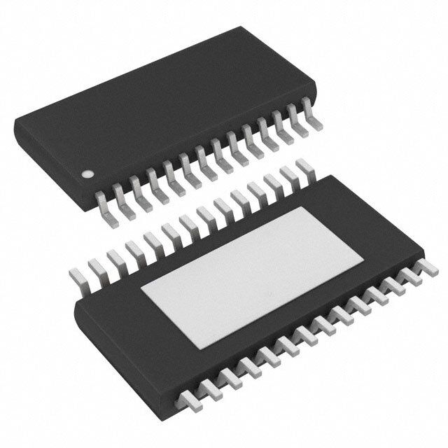
ICGOO电子元器件商城为您提供BD63875EFV-E2由ROHM Semiconductor设计生产,在icgoo商城现货销售,并且可以通过原厂、代理商等渠道进行代购。 BD63875EFV-E2价格参考¥61.78-¥61.78。ROHM SemiconductorBD63875EFV-E2封装/规格:PMIC - 电机驱动器,控制器, 双极性 电机驱动器 DMOS 串行 28-HTSSOP-B。您可以下载BD63875EFV-E2参考资料、Datasheet数据手册功能说明书,资料中有BD63875EFV-E2 详细功能的应用电路图电压和使用方法及教程。
| 参数 | 数值 |
| 产品目录 | 集成电路 (IC) |
| 描述 | IC MOTOR DRIVER PWM 28HTSSOP |
| 产品分类 | PMIC - 电机, 电桥式驱动器 |
| 品牌 | Rohm Semiconductor |
| 数据手册 | |
| 产品图片 |
|
| 产品型号 | BD63875EFV-E2 |
| rohs | 无铅 / 符合限制有害物质指令(RoHS)规范要求 |
| 产品系列 | - |
| 产品培训模块 | http://www.digikey.cn/PTM/IndividualPTM.page?site=cn&lang=zhs&ptm=25151 |
| 供应商器件封装 | 28-HTSSOP-B |
| 其它名称 | BD63875EFV-E2CT |
| 功能 | 驱动器 - 全集成,控制和功率级 |
| 包装 | 剪切带 (CT) |
| 安装类型 | 表面贴装 |
| 封装/外壳 | 28-SOIC(0.173",4.40mm 宽)裸露焊盘 |
| 工作温度 | -25°C ~ 85°C |
| 应用 | 通用 |
| 接口 | PWM |
| 标准包装 | 1 |
| 特色产品 | http://www.digikey.com/cn/zh/ph/ROHM/stepper_motor_drivers.html |
| 电压-电源 | 19 V ~ 28 V |
| 电压-负载 | 19 V ~ 28 V |
| 电机类型-AC,DC | - |
| 电机类型-步进 | 双极性 |
| 电流-输出 | 1.2A |
| 输出配置 | 全 H 桥,(2) 双 |


- 商务部:美国ITC正式对集成电路等产品启动337调查
- 曝三星4nm工艺存在良率问题 高通将骁龙8 Gen1或转产台积电
- 太阳诱电将投资9.5亿元在常州建新厂生产MLCC 预计2023年完工
- 英特尔发布欧洲新工厂建设计划 深化IDM 2.0 战略
- 台积电先进制程称霸业界 有大客户加持明年业绩稳了
- 达到5530亿美元!SIA预计今年全球半导体销售额将创下新高
- 英特尔拟将自动驾驶子公司Mobileye上市 估值或超500亿美元
- 三星加码芯片和SET,合并消费电子和移动部门,撤换高东真等 CEO
- 三星电子宣布重大人事变动 还合并消费电子和移动部门
- 海关总署:前11个月进口集成电路产品价值2.52万亿元 增长14.8%


PDF Datasheet 数据手册内容提取
Stepping Motor Driver series High Performance, High Reliability 36V Series Stepping Motor Drivers BD6387xEFV Series No.12009EAT10 ●Description BD6387xEFV series are the high-grade type that provides the highest function and highest reliance in the ROHM stepping motor driver series. As for its basic function, it is a low power consumption bipolar PWM constant current-drive driver with power BD63877/BD63875/BD63873EFV are CLK-IN type drivers and BD63876/BD63874/BD63872EFV are PARALLEL-IN type drivers. There are excitation modes of FULL STEP & HALF STEP (2 kinds), QUARTER STEP mode, and for current decay mode, the ratio of FAST DECAY & SLOW DECAY can be freely set, so the optimum control conditions for every motor can be realized. In addition, being able to drive with one system of power supply makes contribution to the set design’s getting easy. ●Feature 1) Single power supply input (rated voltage of 36V) 2) Rated output current:(DC) 1.0A, 1.5A, 2.0A 3) Low ON resistance DMOS output 4) CLK-IN drive mode (BD63877/63875/63873EFV) 5) PARALLEL-IN drive mode (BD63876/63874/63872EFV) 6) PWM constant current control (other oscillation) 7) Built-in spike noise cancel function (external noise filter is unnecessary) 8) Full-, half (two kinds)-, quarter-step functionality 9) Current decay mode switching function (linearly variable FAST/SLOW DECAY ratio) 10) Normal rotation & reverse rotation switching function (BD63877/63875/63873EFV) 11) Power save function 12) Built-in logic input pull-down resistor 13) Power-on reset function (BD63877/63875/63873EFV) 14) Thermal shutdown circuit (TSD) 15) Over current protection circuit (OCP) 16) Under voltage lock out circuit (UVLO) 17) Over voltage lock out circuit (OVLO) 18) Ghost Supply Prevention (protects against malfunction when power supply is disconnected) 19) Electrostatic discharge: 8kV (HBM specification) 20) Adjacent pins short protection 21) Inverted mounting protection 22) Microminiature, ultra-thin and high heat-radiation (exposed metal type) HTSSOP-B28 package 23) Pin-compatible line-up (BD63877/63875/63873EFV, BD63876/63874/63872EFV) ●Application PPC, multi-function printer, laser beam printer, ink jet printer, monitoring camera, WEB camera, sewing machine, photo printer, FAX, scanner, mini printer, toy, and robot etc. www.rohm.com 1/8 2012.02 - Rev.A © 2012 ROHM Co., Ltd. All rights reserved.
BD6387xEFV Series Technical Note ●Absolute maximum ratings(Ta=25℃) Item Symbol BD63877/63876EFV BD63875/63874EFV BD63873/63872EFV Unit Supply voltage V -0.2~+36.0 V CC1,2 1.45※1 W Power dissipation Pd 4.70※2 W Input voltage for control pin V -0.2~+5.5 V IN RNF maximum voltage V 0.7 V RNF Maximum output current I 2.0※3 1.5※3 1.0※3 A/phase OUT Maximum output current (PEAK)※4 I 2.5※3 2.0※3 1.5※3 A/phase OUTPEAK Operating temperature range T -25~+85 ℃ opr Storage temperature range T -55~+150 ℃ stg Junction temperature T +150 ℃ jmax ※1 70mm ×70mm×1.6mm glass epoxy board. Derating in done at 11.6mW/℃ for operating above Ta=25℃. ※2 4-layer recommended board. Derating in done at 37.6mW/ ℃ for operating above Ta=25℃. ※3 Do not, however exceed Pd, ASO and Tjmax=150 ℃. ※4 Pulse width tw ≦1ms, duty 20%. ●Operating conditions(Ta= -25~+85℃) Item Symbol BD63877/63876EFV BD63875/63874EFV BD63873/63872EFV Unit Supply voltage V 19~28 V CC1,2 MaximumOutput current (DC) I 1.7※5 1.2※5 0.7※5 A/phase OUT ※5 Do not, however exceed Pd, ASO and . ●Electrical characteristics (Unless otherwise specified Ta=25℃, V =24V) CC1,2 Limit Item Symbol Unit Conditions Min. Typ. Max. Whole Circuit current at standby I - 1.0 2.5 mA PS=L CCST Circuit current I - 2.5 5.0 mA PS=H, VREF=3V CC Control input H level input voltage V 2.0 - - V INH L level input voltage V - - 0.8 V INL H level input current I 35 50 100 μA V =5V INH IN L level input current I -10 0 - μA V =0V INL IN Output (OUT1A, OUT1B, OUT2A, OUT2B) I =1.5A, Output ON resistance (BD63877/63876EFV) R - 0.65 0.85 Ω OUT ON Sum of upper and lower I =1.0A, Output ON resistance (BD63875/63874EFV) R - 1.00 1.30 Ω OUT ON Sum of upper and lower I =0.5A, Output ON resistance (BD63873/63872EFV) R - 1.90 2.47 Ω OUT ON Sum of upper and lower Output leak current I - - 10 μA LEAK Current control RNFXS input current I -2.0 -0.1 - μA RNFXS=0V RNFS RNFX input current I -40 -20 - μA RNFX=0V RNF VREF input current I -2.0 -0.1 - μA VREF=0V VREF VREF input voltage range V 0 - 3.0 V REF MTH input current I -2.0 -0.1 - μA MTH=0V MTH MTH input voltage range V 0 - 3.5 V MTH Minimum on time (Blank time) t 0.3 0.8 1.5 μs C=1000pF, R=39kΩ ONMIN BD63877EFV/63875EFV/63873EFV Comparator threshold V 0.57 0.60 0.63 V VREF=3V CTH BD63876EFV/63874EFV/63872EFV V Comparator threshold 100% CTH10 0.57 0.60 0.63 V VREF=3V, (I0X,I1X)=(L,L) 0 VREF=3V, Comparator threshold 67% V 0.38 0.40 0.42 V CTH67 (I0X,I1X)=(H,L) VREF=3V, Comparator threshold 33% V 0.18 0.20 0.22 V CTH33 (I0X,I1X)=(L,H) www.rohm.com 2/8 2012.02 - Rev.A © 2012 ROHM Co., Ltd. All rights reserved.
BD6387xEFV Series Technical Note ●Terminal function and Application circuit diagram CLK-IN type (BD63877/63875/63873EFV) Pin Pin Pin name Function Pin name Function No. No. Clock input terminal for advancing the 1 GND Ground terminal 15 CLK electrical angle. 2 OUT1B H bridge output terminal 16 CW_CCW Motor rotating direction setting terminal Connection terminal of resistor for output Terminal for testing 3 RNF1 current detection 17 TEST (used by connecting with GND) 4 RNF1S Input terminal of current limit comparator 18 MODE0 Motor excitation mode setting terminal 5 OUT1A H bridge output terminal 19 MODE1 Motor excitation mode setting terminal 6 NC Non connection 20 ENABLE Power supply terminal 7 VCC1 Power supply terminal 21 NC Non connection 8 NC Non connection 22 VCC2 Power supply terminal 9 GND Ground terminal 23 NC Non connection Connection terminal of CR for setting 10 CR chopping frequency 24 OUT2A H bridge output terminal 11 NC Non connection 25 RNF2S Input terminal of current limit comparator Connection terminal of resistor for output 12 MTH Current decay mode setting terminal 26 RNF2 current detection 13 VREF Output current value setting terminal 27 OUT2B H bridge output terminal 14 PS Power save terminal 28 NC Non connection Logic input terminal. Refer to P.6 for detail. Power save terminal CLK 15 Regulator Refer to P.6 for detail. CW_CCW16 9 GND MODE018 Translator MODE119 RESET 14PS ENABLE UVLO 20 OVLO TSD Bypass capacitor. + Setting range is VREF13 - 2bit DAC OCP 100uF~470uF(electrolytic) 0.01uF~0.1uF(multilayer ceramic etc.) SIneptu tth bey o ruetspiustt ocru drriveinseotn. . Refer to P.7 for detail. Refer to P.8 for detail. 7 VCC1 Be sure to short VCC1 & VCC2. +- 5 OUT1A Set the chopping RNF1S 2 fSreeqttuinegn crayn. ge is + 3 OUT1B 0.2Ω C:470pF~1500pF RNF2S - c RNF1 100uF 0.1uF RR:e1f0ekr Ωto ~P.280, 09k fΩor detail. PBWlaMn kc otinmtreo l ontrol logi Predriver 242RVCNCF12S CR10 OSC C 24OUT2A Resistor for current. detecting. 39kΩ 1000pF 27 Setting range is OUT2B 0.1Ω~0.3Ω. MTH12 Mcixo ndtercoal y 26RNF2 0.2Ω Refer to P.7 for detail. Set th e current decay mode. 25RNF2S ①SL OW DECAY TEST17 GND ⇒Co nnect to GND. 1 ②MIX DECAY ⇒Input by resistor divison. Resistor for current. detecting. Refer to P.8, 10 for detail. Setting range is Terminal for testing. 0.1Ω~0.3Ω. Refer to P.7 for detail. Connect to GND. Fig.1Block diagram & Application circuit diagram of BD63877EFV/BD63875EFV/BD63873EFV www.rohm.com 3/8 2012.02 - Rev.A © 2012 ROHM Co., Ltd. All rights reserved.
BD6387xEFV Series Technical Note PARALLEL-IN type (BD63876/63874/63872EFV) Pin Pin Pin name Function Pin name Function No. No. 1 GND Ground terminal 15 PHASE1 Phase selection terminal 2 OUT1B H bridge output terminal 16 I01 VREF division ratio setting terminal Connection terminal of resistor for output 3 RNF1 current detection 17 I11 VREF division ratio setting terminal 4 RNF1S Input terminal of current limit comparator 18 PHASE2 Phase selection pin 5 OUT1A H bridge output terminal 19 I02 VREF division ratio setting terminal 6 NC Non connection 20 I12 VREF division ratio setting terminal 7 VCC1 Power supply terminal 21 NC Non connection 8 NC Non connection 22 VCC2 Power supply terminal 9 GND Ground terminal 23 NC Non connection Connection terminal of CR for setting 10 CR chopping frequency 24 OUT2A H bridge output terminal 11 NC Non connection 25 RNF2S Input terminal of current limit comparator Connection terminal of resistor for output 12 MTH Current decay mode setting terminal 26 RNF2 current detection 13 VREF Output current value setting terminal 27 OUT2B H bridge output terminal 14 PS Power save terminal 28 NC Non connection Logic input terminal. Refer to P.7 for detail. Power save terminal Refer to P.7 for detail. 15 PHASE1 Regulator PHASE2 GND 1168 9 I01 17 14PS I11 19 UVLO I02 I1220 OVLO Bypass capacitor. + TSD Setting range is VREF13 - 100uF~470uF(electrolytic) 2bit DAC OCP 0.01uF~0.1uF(multilayer ceramic etc.) Set the output currenet. Refer to P.7 for detail. Input by resistor divison. Be sure to short VCC1 & VCC2. VCC1 Refer to P.8 for detail. 7 + OUT1A - 5 Set the chopping RNF1S 2 fSreeqttuinegn crayn. ge is + 3 OUT1B 0.2Ω C:470pF~1500pF RNF2S - c RNF1 100uF 0.1uF RでR:1すf0。kΩt ~P28009kfΩ d t il PBWlaMn kc otinmtreo l ontrol logi Predriver 242RVCNCF12S CR10 OSC C 24OUT2A Resistor for current. detecting. 39kΩ 1000pF 27 Setting range is OUT2B 0.1Ω~0.3Ω. MTH12 Mcixo ndtercoal y 26RNF2 0.2Ω Refer to P.7 for detail. 25 S et the current decay mode. RNF2S ① SLOW DECAY GND ⇒Connect to GND. 1 ② MIX DECAY ⇒Input by resistor divison. Resistor for current. detecting. R efer to P.8, 10 for detail. Setting range is 0.1Ω~0.3Ω. Refer to P.7 for detail. Fig.2Block diagram & Application circuit diagram of BD63876FV/BD63874FV/BD63872FV www.rohm.com 4/8 2012.02 - Rev.A © 2012 ROHM Co., Ltd. All rights reserved.
BD6387xEFV Series Technical Note ●Points to notice for terminal description ○CLK/Clock input terminal for advancing the electrical angle(BD63877/BD63875/BD63873EFV) CLK is reflected at rising edge. The Electrical angle advances by one for each CLK input. Motor’s misstep will occur if noise is picked up at the CLK terminal, so please design the pattern in such a way that there is no noise plunging. ○MODE0,MODE1/Motor excitation mode setting terminal (BD63877/BD63875/BD63873EFV) Set the motor excitation mode. MODE0 MODE1 Excitation mode L L FULL STEP H L HALF STEP A L H HALF STEP B H H QUARTER STEP ○CW_CCW Terminal/Motor rotating direction setting terminal (BD63877/BD63875/BD63873EFV) Set the motor’s rotating direction. Change in setting is reflected at the CLK rising edge immediately after the change in setting CW_CCW Rotating direction L Clockwise (CH2’s current is outputted with a phase lag of 90°in regard to CH1’s current) Counter Clockwise(CH2’s current is outputted with a phase lead of 90°in regard to CH1’s H current) ○ENABLE Terminal/Output enable terminal (BD63877/BD63875/BD63873EFV) Turn off forcibly all the output transistors (motor output is open). At the time of ENABLE=L, electrical angle or operating mode is maintained even if CLK is inputted. Please be careful because the electrical angle at the time of ENABLE being released (ENABLE=L→H) is different from the released occasion at the section of CLK=H and from the released occasion at the section of CLK=L ENABLE Motor output L OPEN (electrical angle maintained) H ACTIVE ○PS/Power save terminal (BD63877/BD63875/BD63873EFV) PS can make circuit standby state and make motor output OPEN. In standby state, translator circuit is reset (initialized) and electrical angle is initialized. Please be careful because there is a delay of 40μs(max.) before it is returned from standby state to normal state and the motor output becomes ACTIVE PS State L Standby state (RESET) H ACTIVE The electrical angle (initial electrical angle) of each excitation mode immediately after RESET is as follows Please be careful because the initial state at the time of FULL STEP is different from those of other excitation modes. Excitation mode Initial electrical angle FULL STEP 45° HALFSTEP A 0° HALFSTEP B 0° QUARTER 0° STEP ●Protection Circuits ○Thermal Shutdown (TSD) This IC has a built-in thermal shutdown circuit for thermal protection. When the IC’s chip temperature rises above 175℃ (Typ.), the motor output becomes OPEN. Also, when the temperature returns to under 150℃ (Typ.), it automatically returns to normal operation. However, even when TSD is in operation, if heat is continued to be added externally, heat overdrive can lead to destruction. www.rohm.com 5/8 2012.02 - Rev.A © 2012 ROHM Co., Ltd. All rights reserved.
BD6387xEFV Series Technical Note ○Over Current Protection (OCP) This IC has a built in over current protection circuit as a provision against destruction when the motor outputs are shorted each other or VCC-motor output or motor output-GND is shorted. This circuit latches the motor output to OPEN condition when the regulated threshold current flows for 4μs (Typ.). It returns with power reactivation or a reset of the PS terminal. The over current protection circuit’s only aim is to prevent the destruction of the IC from irregular situations such as motor output shorts, and is not meant to be used as protection or security for the set. Therefore, sets should not be designed to take into account this circuit’s functions. After OCP operating, if irregular situations continues and the return by power reactivation or a reset of the PS terminal is carried out repeatly, then OCP operates repeatly and the IC may generate heat or otherwise deteriorate. When the L value of the wiring is great due to the wiring being long, after the over current has flowed and the output terminal voltage jumps up and the absolute maximum values may be exceeded and as a result, there is a possibility of destruction. Also, when current which is over the output current rating and under the OCP detection current flows, the IC can heat up to over Tjmax=150℃ and can deteriorate, so current which exceeds the output rating should not be applied. ○Under Voltage Lock Out (UVLO) This IC has a built-in under voltage lock out function to prevent false operation such as IC output during power supply under voltage. When the applied voltage to the VCC terminal goes under 15V (Typ.), the motor output is set to OPEN. This switching voltage has a 1V (Typ.) hysteresis to prevent false operation by noise etc. Please be aware that this circuit does not operate during power save mode. Also, the electrical angle is reset when the UVLO circuit operates during CLK-IN drive mode. ○Over Voltage Lock Out (OVLO) This IC has a built-in over voltage lock out function to protect the IC output and the motor during power supply over voltage. When the applied voltage to the VCC terminal goes over 32V (Typ.), the motor output is set to OPEN. This switching voltage has a 1V (Typ.) hysteresis and a 4μs (Typ.) mask time to prevent false operation by noise etc. Although this over voltage locked out circuit is built-in, there is a possibility of destruction if the absolute maximum value for power supply voltage is exceeded, therefore the absolute maximum value should not be exceeded. Please be aware that this circuit does not operate during power save mode. ○Ghost Supply Prevention (protects against malfunction when power supply is disconnected) If a signal (logic input, VREF, MTH) is input when there is no power supplied to this IC, there is a function which prevents the false operation by voltage supplied via the electrostatic destruction prevention diode from these input terminals to the VCC to this IC or to another IC’s power supply. Therefore, there is no malfunction of the circuit even when voltage is supplied to these input terminals while there is no power supply. ●Usage Notes (1) Absolute maximum ratings An excess in the absolute maximum ratings, such as supply voltage, temperature range of operating conditions, etc., can break down the devices, thus making impossible to identify breaking mode, such as a short circuit or an open circuit. If any over rated values will expect to exceed the absolute maximum ratings, consider adding circuit protection devices, such as fuses. (2) Connecting the power supply connector backward Connecting of the power supply in reverse polarity can damage IC. Take precautions when connecting the power supply lines. An external direction diode can be added. (3) Power supply Lines Design PCB layout pattern to provide low impedance GND and supply lines. To obtain a low noise ground and supply line, separate the ground section and supply lines of the digital and analog blocks. Furthermore, for all power supply terminals to ICs, connect a capacitor between the power supply and the GND terminal. When applying electrolytic capacitors in the circuit, not that capacitance characteristic values are reduced at low temperatures. (4) GND Potential The potential of GND pin must be minimum potential in all operating conditions. (5) Metal on the backside (Define the side where product markings are printed as front) The metal on the backside is shorted with the backside of IC chip therefore it should be connected to GND. Be aware that there is a possibility of malfunction or destruction if it is shorted with any potential other than GND. (6) Thermal design Use a thermal design that allows for a sufficient margin in light of the power dissipation (Pd) in actual operating conditions. Users should be aware that these products have been designed to expose their frames at the back of the package, and should be used with suitable heat dissipation treatment in this area to improve dissipation. As large a dissipation pattern should be taken as possible, not only on the front of the baseboard but also on the back surface. It is important to consider actual usage conditions and to take as large a dissipation pattern as possible. www.rohm.com 6/8 2012.02 - Rev.A © 2012 ROHM Co., Ltd. All rights reserved.
BD6387xEFV Series Technical Note (7) Inter-pin shorts and mounting errors When attaching to a printed circuit board, pay close attention to the direction of the IC and displacement. Improper attachment may lead to destruction of the IC. There is also possibility of destruction from short circuits which can be caused by foreign matter entering between outputs or an output and the power supply or GND. (8) Operation in a strong electric field Use caution when using the IC in the presence of a strong electromagnetic field as doing so may cause the IC to malfunction. (9) ASO When using the IC, set the output transistor so that it does not exceed absolute maximum ratings or ASO. (10) Thermal shutdown circuit The IC has a built-in thermal shutdown circuit (TSD circuit). If the chip temperature becomes Tjmax=150℃, and higher, coil output to the motor will be open. The TSD circuit is designed only to shut the IC off to prevent runaway thermal operation. It is not designed to protect or indemnify peripheral equipment. Do not use the TSD function to protect peripheral equipment. TSD on temperature [℃] (Typ.) Hysteresis Temperature [℃] (Typ.) 175 25 (11) Inspection of the application board During inspection of the application board, if a capacitor is connected to a pin with low impedance there is a possibility that it could cause stress to the IC, therefore an electrical discharge should be performed after each process. Also, as a measure again electrostatic discharge, it should be earthed during the assembly process and special care should be taken during transport or storage. Furthermore, when connecting to the jig during the inspection process, the power supply should first be turned off and then removed before the inspection. (12) Input terminal of IC This IC is a monolithic IC, and between each element there is a P+ isolation for element partition and a P substrate. This P layer and each element’s N layer make up the P-N junction, and various parasitic elements are made up. For example, when the resistance and transistor are connected to the terminal as shown in figure 3, ○When GND>(Terminal A) at the resistance and GND>(Terminal B) at the transistor (NPN), the P-N junction operates as a parasitic diode. ○Also, when GND>(Terminal B) at the transistor (NPN) The parasitic NPN transistor operates with the N layers of other elements close to the aforementioned parasitic diode. Because of the IC’s structure, the creation of parasitic elements is inevitable from the electrical potential relationship. The operation of parasitic elements causes interference in circuit operation, and can lead to malfunction and destruction. Therefore, be careful not to use it in a way which causes the parasitic elements to operate, such as by applying voltage that is lower than the GND (P substrate) to the input terminal. Resistor Transistor (NPN) Pin A Pin B Pin B B C Pin A E C P+ N P+ N P+ N P P+ B N P N Parasitic N element E P substrate P substrate Parasitic element GND Parasitic element GND Parasitic element GND GND Other adjacent elements Fig. 3 Pattern Diagram of Parasitic Element (13) Ground Wiring Patterns When using both small signal and large current GND patterns, it is recommended to isolate the two ground patterns, placing a single ground point at the application's reference point so that the pattern wiring resistance and voltage variations caused by large currents do not cause variations in the small signal ground voltage. Be careful not to change the GND wiring pattern potential of any external components, either. (14) TEST Terminal (BD63877/BD63875/BD63873EFV) Be sure to connect TEST pin to GND. www.rohm.com 7/8 2012.02 - Rev.A © 2012 ROHM Co., Ltd. All rights reserved.
BD6387xEFV Series Technical Note ●Ordering part number B D 6 3 8 7 2 E F V - E 2 形名 パッケージ 包装、フォーミング仕様 EFV=HTSSOP-B28 E2: リール状エンボステーピング HTSSOP-B28 <Tape and Reel information> 9.7±0.1 (MAX 10.05 include BURR) Tape Embossed carrier tape (with dry pack) (5.5) 4°+−64°° Quantity 2500pcs 28 15 ±6.40.2 ±4.40.1 (2.9) ±0.50.15 ±1.00.2 Dofi rfeecetdion E(2Treheel odnir ethcteio lne fits h tahned 1 apnind oyfo pur opduull cot uist tahte t htaep uep opne rt hleef tr iwghhte hna ynodu hold ) 1 14 0.625 1PIN MARK +0.05 0.17-0.03 AX S M 1.0 ±0.850.05 ±0.080.05 0.65 0.24-+00..0045 0.00.808SM 1pin Direction of feed (Unit : mm) Reel ∗ Order quantity needs to be multiple of the minimum quantity. www.rohm.com 8/8 2012.02 - Rev.A © 2012 ROHM Co., Ltd. All rights reserved.
DDaattaasshheeeett Notice Precaution on using ROHM Products 1. Our Products are designed and manufactured for application in ordinary electronic equipments (such as AV equipment, OA equipment, telecommunication equipment, home electronic appliances, amusement equipment, etc.). If you intend to use our Products in devices requiring extremely high reliability (such as medical equipment (Note 1), transport equipment, traffic equipment, aircraft/spacecraft, nuclear power controllers, fuel controllers, car equipment including car accessories, safety devices, etc.) and whose malfunction or failure may cause loss of human life, bodily injury or serious damage to property (“Specific Applications”), please consult with the ROHM sales representative in advance. Unless otherwise agreed in writing by ROHM in advance, ROHM shall not be in any way responsible or liable for any damages, expenses or losses incurred by you or third parties arising from the use of any ROHM’s Products for Specific Applications. (Note1) Medical Equipment Classification of the Specific Applications JAPAN USA EU CHINA CLASSⅢ CLASSⅡb CLASSⅢ CLASSⅢ CLASSⅣ CLASSⅢ 2. ROHM designs and manufactures its Products subject to strict quality control system. However, semiconductor products can fail or malfunction at a certain rate. Please be sure to implement, at your own responsibilities, adequate safety measures including but not limited to fail-safe design against the physical injury, damage to any property, which a failure or malfunction of our Products may cause. The following are examples of safety measures: [a] Installation of protection circuits or other protective devices to improve system safety [b] Installation of redundant circuits to reduce the impact of single or multiple circuit failure 3. Our Products are designed and manufactured for use under standard conditions and not under any special or extraordinary environments or conditions, as exemplified below. Accordingly, ROHM shall not be in any way responsible or liable for any damages, expenses or losses arising from the use of any ROHM’s Products under any special or extraordinary environments or conditions. If you intend to use our Products under any special or extraordinary environments or conditions (as exemplified below), your independent verification and confirmation of product performance, reliability, etc, prior to use, must be necessary: [a] Use of our Products in any types of liquid, including water, oils, chemicals, and organic solvents [b] Use of our Products outdoors or in places where the Products are exposed to direct sunlight or dust [c] Use of our Products in places where the Products are exposed to sea wind or corrosive gases, including Cl2, H2S, NH3, SO2, and NO2 [d] Use of our Products in places where the Products are exposed to static electricity or electromagnetic waves [e] Use of our Products in proximity to heat-producing components, plastic cords, or other flammable items [f] Sealing or coating our Products with resin or other coating materials [g] Use of our Products without cleaning residue of flux (even if you use no-clean type fluxes, cleaning residue of flux is recommended); or Washing our Products by using water or water-soluble cleaning agents for cleaning residue after soldering [h] Use of the Products in places subject to dew condensation 4. The Products are not subject to radiation-proof design. 5. Please verify and confirm characteristics of the final or mounted products in using the Products. 6. In particular, if a transient load (a large amount of load applied in a short period of time, such as pulse. is applied, confirmation of performance characteristics after on-board mounting is strongly recommended. Avoid applying power exceeding normal rated power; exceeding the power rating under steady-state loading condition may negatively affect product performance and reliability. 7. De-rate Power Dissipation (Pd) depending on Ambient temperature (Ta). When used in sealed area, confirm the actual ambient temperature. 8. Confirm that operation temperature is within the specified range described in the product specification. 9. ROHM shall not be in any way responsible or liable for failure induced under deviant condition from what is defined in this document. Precaution for Mounting / Circuit board design 1. When a highly active halogenous (chlorine, bromine, etc.) flux is used, the residue of flux may negatively affect product performance and reliability. 2. In principle, the reflow soldering method must be used; if flow soldering method is preferred, please consult with the ROHM representative in advance. For details, please refer to ROHM Mounting specification Notice - GE Rev.002 © 2014 ROHM Co., Ltd. All rights reserved.
DDaattaasshheeeett Precautions Regarding Application Examples and External Circuits 1. If change is made to the constant of an external circuit, please allow a sufficient margin considering variations of the characteristics of the Products and external components, including transient characteristics, as well as static characteristics. 2. You agree that application notes, reference designs, and associated data and information contained in this document are presented only as guidance for Products use. Therefore, in case you use such information, you are solely responsible for it and you must exercise your own independent verification and judgment in the use of such information contained in this document. ROHM shall not be in any way responsible or liable for any damages, expenses or losses incurred by you or third parties arising from the use of such information. Precaution for Electrostatic This Product is electrostatic sensitive product, which may be damaged due to electrostatic discharge. Please take proper caution in your manufacturing process and storage so that voltage exceeding the Products maximum rating will not be applied to Products. Please take special care under dry condition (e.g. Grounding of human body / equipment / solder iron, isolation from charged objects, setting of Ionizer, friction prevention and temperature / humidity control). Precaution for Storage / Transportation 1. Product performance and soldered connections may deteriorate if the Products are stored in the places where: [a] the Products are exposed to sea winds or corrosive gases, including Cl2, H2S, NH3, SO2, and NO2 [b] the temperature or humidity exceeds those recommended by ROHM [c] the Products are exposed to direct sunshine or condensation [d] the Products are exposed to high Electrostatic 2. Even under ROHM recommended storage condition, solderability of products out of recommended storage time period may be degraded. It is strongly recommended to confirm solderability before using Products of which storage time is exceeding the recommended storage time period. 3. Store / transport cartons in the correct direction, which is indicated on a carton with a symbol. Otherwise bent leads may occur due to excessive stress applied when dropping of a carton. 4. Use Products within the specified time after opening a humidity barrier bag. Baking is required before using Products of which storage time is exceeding the recommended storage time period. Precaution for Product Label QR code printed on ROHM Products label is for ROHM’s internal use only. Precaution for Disposition When disposing Products please dispose them properly using an authorized industry waste company. Precaution for Foreign Exchange and Foreign Trade act Since our Products might fall under controlled goods prescribed by the applicable foreign exchange and foreign trade act, please consult with ROHM representative in case of export. Precaution Regarding Intellectual Property Rights 1. All information and data including but not limited to application example contained in this document is for reference only. ROHM does not warrant that foregoing information or data will not infringe any intellectual property rights or any other rights of any third party regarding such information or data. ROHM shall not be in any way responsible or liable for infringement of any intellectual property rights or other damages arising from use of such information or data.: 2. No license, expressly or implied, is granted hereby under any intellectual property rights or other rights of ROHM or any third parties with respect to the information contained in this document. Other Precaution 1. This document may not be reprinted or reproduced, in whole or in part, without prior written consent of ROHM. 2. The Products may not be disassembled, converted, modified, reproduced or otherwise changed without prior written consent of ROHM. 3. In no event shall you use in any way whatsoever the Products and the related technical information contained in the Products or this document for any military purposes, including but not limited to, the development of mass-destruction weapons. 4. The proper names of companies or products described in this document are trademarks or registered trademarks of ROHM, its affiliated companies or third parties. Notice - GE Rev.002 © 2014 ROHM Co., Ltd. All rights reserved.
DDaattaasshheeeett General Precaution 1. Before you use our Products, you are requested to carefully read this document and fully understand its contents. ROHM shall not be in any way responsible or liable for failure, malfunction or accident arising from the use of a ny ROHM’s Products against warning, caution or note contained in this document. 2. All information contained in this document is current as of the issuing date and subj ect to change without any prior notice. Before purchasing or using ROHM’s Products, please confirm the latest information with a ROHM sale s representative. 3. The information contained in this document is provided on an “as is” basis and ROHM does not warrant that all information contained in this document is accurate an d/or error-free. ROHM shall not be in any way responsible or liable for any damages, expenses or losses incurred by you or third parties resulting from inaccuracy or errors of or concerning such information. Notice – WE Rev.001 © 2014 ROHM Co., Ltd. All rights reserved.
Mouser Electronics Authorized Distributor Click to View Pricing, Inventory, Delivery & Lifecycle Information: R OHM Semiconductor: BD63876EFV-E2 BD63872EFV-E2 BD63874EFV-E2 BD63877EFV-E2