ICGOO在线商城 > BD1604MVV-E2

 Datasheet下载
- 型号: BD1604MVV-E2
- 制造商: ROHM Semiconductor
- 库位|库存: xxxx|xxxx
- 要求:
| 数量阶梯 | 香港交货 | 国内含税 |
| +xxxx | $xxxx | ¥xxxx |
查看当月历史价格
查看今年历史价格
BD1604MVV-E2产品简介:
ICGOO电子元器件商城为您提供BD1604MVV-E2由ROHM Semiconductor设计生产,在icgoo商城现货销售,并且可以通过原厂、代理商等渠道进行代购。 提供BD1604MVV-E2价格参考以及ROHM SemiconductorBD1604MVV-E2封装/规格参数等产品信息。 你可以下载BD1604MVV-E2参考资料、Datasheet数据手册功能说明书, 资料中有BD1604MVV-E2详细功能的应用电路图电压和使用方法及教程。
| 参数 | 数值 |
| 产品目录 | 集成电路 (IC)光电子产品 |
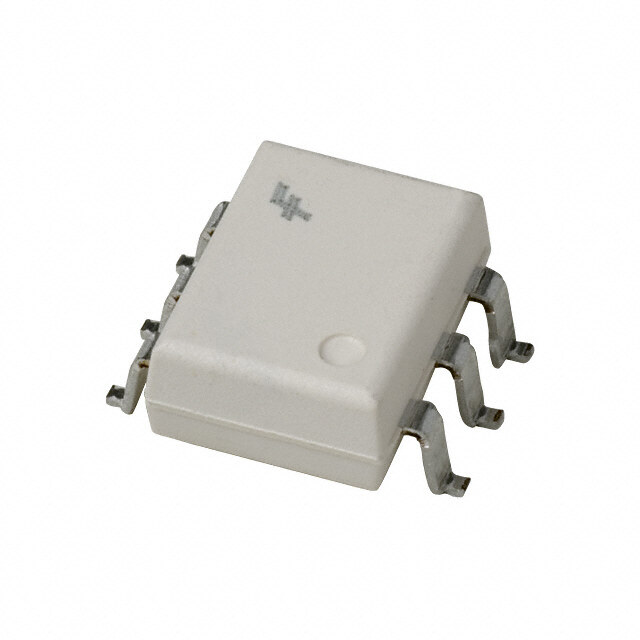
| 描述 | IC LED DRVR WHITE BCKLGT 16-SQFNLED照明驱动器 Backlight LED Driver for Small Panel |
| 产品分类 | |
| 品牌 | ROHM Semiconductor |
| 产品手册 | |
| 产品图片 |
|
| rohs | 符合RoHS无铅 / 符合限制有害物质指令(RoHS)规范要求 |
| 产品系列 | LED照明电子器件,LED照明驱动器,ROHM Semiconductor BD1604MVV-E2- |
| 数据手册 | |
| 产品型号 | BD1604MVV-E2 |
| 产品目录页面 | |
| 产品种类 | LED照明驱动器 |
| 供应商器件封装 | SQFN016V4040 |
| 其它名称 | BD1604MVV-E2DKR |
| 内部驱动器 | 是 |
| 功率耗散 | 780 mW |
| 包装 | Digi-Reel® |
| 商标 | ROHM Semiconductor |
| 安装类型 | 表面贴装 |
| 安装风格 | SMD/SMT |
| 封装 | Reel |
| 封装/外壳 | 16-VQFN 裸露焊盘 |
| 封装/箱体 | SQFN-16 |
| 工作温度 | -30°C ~ 85°C |
| 工厂包装数量 | 2500 |
| 恒压 | - |
| 恒流 | - |
| 拓扑 | PWM,切换式电容器(充电泵) |
| 最大工作温度 | + 85 C |
| 最小工作温度 | - 30 C |
| 标准包装 | 1 |
| 电压-电源 | 2.7 V ~ 5.5 V |
| 电压-输出 | 5V |
| 类型-初级 | 背光 |
| 类型-次级 | 白色 LED |
| 输入电压 | 2.7 V to 5.5 V |
| 输出数 | 4 |
| 频率 | 800kHz ~ 1.2MHz |


- 商务部:美国ITC正式对集成电路等产品启动337调查
- 曝三星4nm工艺存在良率问题 高通将骁龙8 Gen1或转产台积电
- 太阳诱电将投资9.5亿元在常州建新厂生产MLCC 预计2023年完工
- 英特尔发布欧洲新工厂建设计划 深化IDM 2.0 战略
- 台积电先进制程称霸业界 有大客户加持明年业绩稳了
- 达到5530亿美元!SIA预计今年全球半导体销售额将创下新高
- 英特尔拟将自动驾驶子公司Mobileye上市 估值或超500亿美元
- 三星加码芯片和SET,合并消费电子和移动部门,撤换高东真等 CEO
- 三星电子宣布重大人事变动 还合并消费电子和移动部门
- 海关总署:前11个月进口集成电路产品价值2.52万亿元 增长14.8%


PDF Datasheet 数据手册内容提取
LED Drivers for LCD Backlights Backlight LED Drivers for Small LCD Panels (Charge Pump Type) BD1604MUV, BD1604MVV No.11040EBT23 ●Description This LSI is a 4 white LED driver for small LCD backlight. At the charge pump type, the number of external devices is minimized. ●Features 1) 4 parallel LED driver is mounted. 2) The LED current can be controlled via an external resistance. 3) Maximum current is 120mA (30mA × 4). 4) LED1 to LED4 can be turned on or off via an external control pin. 5) The relative current accuracy among LEDs (LED1 to LED4) is 3%. 6) Automatically transition to each mode (×1.0, ×1.5, ×2.0). 7) High efficiency (90% or more at maximum) is achieved. 8) Various protection functions such as output voltage protection function, current overload limiter and thermal shutdown circuit are mounted. ●Applications This driver provides for: - Backlight using white LED - Auxiliary lights for mobile phone cameras and simplified flash ●Lineup Parameter BD1604MUV BD1604MVV Number of LED channels 4ch 4ch Maximum current 120mA 120mA VQFN016V3030 SQFN016V4040 Package 3.00mm×3.00mm 4.00mm×4.00mm ●Absolute Maximum Rating (Ta=25℃) Parameter Symbol Ratings Unit Power supply voltage Vmax 7 V BD1604MUV 700 *1 Allowable loss Pd mW BD1604MVV 780 *2 Operating temperature range Topr -30~85 ℃ Storage temperature range Tstr -55~150 ℃ *1 When a glass epoxy substrate (70mm×70mm×1.6mm) has been mounted, this loss will decrease 5.6mW/℃ if Ta is higher than or equal to 25℃. *2 When a glass epoxy substrate (70mm×70mm×1.6mm) has been mounted, this loss will decrease 6.24mW/℃ if Ta is higher than or equal to 25℃. ●Recommended Operation Range Parameter Symbol Limits Unit Condition Operating supply voltage VBAT 2.7~5.5 V VBAT voltage www.rohm.com 1/10 2011.06 - Rev.B © 2011 ROHM Co., Ltd. All rights reserved.
BD1604MUV, BD1604MVV Technical Note ●Electrical Characteristics Unless otherwise specified, Ta is 25℃ and VBAT is 3.6V. Limits Parameter Symbol Unit Condition Min. Typ. Max. [Circuit current] Circuit current 0 IQ0 - 0.1 1 μA EN=0V Circuit current 1.0 IQ1.0 - 1.0 2.0 mA x1.0 Mode, Iout = 0mA Circuit current 1.5 IQ1.5 - 2.3 3.3 mA x1.5 Mode, Iout = 0mA Circuit current 2.0 IQ2.0 - 2.5 3.5 mA X2.0 Mode, Iout = 0mA Unless otherwise specified, Ta is 25℃ and VBAT is 3.6V. Limits Parameter Symbol Unit Condition Min. Typ. Max. [Current driver] LED maximum current ILEDmax - - 30 mA LED current accuracy ILEDdiff - 0.5 5.0 % ILED=10mA LED current matching ILEDmatch - 0.5 3.0 % ILED=10mA *1) Minimum voltage LED pin control voltage VLED 0.08 0.10 0.20 V at LED1~LED4 pins ISET voltage ISET 0.5 0.6 0.7 V Oscillation frequency Fosc 0.8 1.0 1.2 MHz Over current limiter IOV - 600 900 mA LED current limiter ILEDOV 40 60 100 mA *1) LED current matching = (ILEDmax-ILEDmin)/(ILEDmax+ILEDmin)*100 ILEDmax : Maximum value of LED1-4 current ILEDmin : Minimum value of LED1-4 current Unless otherwise specified, Ta is 25℃ and VBAT is 5.5V. Limits Parameter Symbol Unit Condition Min. Typ. Max. [Control Signal etc.] Input ’H’ voltage VIH 1.4 - - V EN,SEL0,SEL1,SEL2 Input ’L’ voltage VIL - - 0.4 V EN,SEL0,SEL1,SEL2 Input ‘H’ current1 IIH1 - 18.3 30 μA EN=5.5V Input ‘H’ current2 IIH2 - 0 1 μA SEL0,SEL1,SEL2=5.5V Input ‘L’ current IIL -1 0 - μA EN,SEL0,SEL1,SEL2=0V Unless otherwise specified, Ta is 25℃ and VBAT is 3.6V. Limits Parameter Symbol Unit Condition Min. Typ. Max. [Control Signal etc.] UVLO detecting voltage VUVLO 1.9 2.2 2.5 V www.rohm.com 2/10 2011.06 - Rev.B © 2011 ROHM Co., Ltd. All rights reserved.
BD1604MUV, BD1604MVV Technical Note ●Reference Data (Evaluation under LED V =3.2V) F 0.5 2 100 STAND-BY Current : Istb [µA]0000....1234 TTTaaa===82-3550℃℃℃ Current Consumption : IQ1.0 [µA]01..551 Ta=25℃T a=85℃ EFFICIENCY [%]5678900000 DOWN UP Ta=-30℃ 0 0 40 3 3.5 4 4.5 5 5.5 0 1 2 3 4 5 2.5 3 3.5 4 4.5 5 5.5 INPUT VOLTAGE : VBAT[V] INPUT VOLTAGE : VBAT[V] SUPPLY VOLTAGE : VBAT[V] Fig.1 Circuit Current Fig.2 Circuit Current Fig.3 Efficiency Hysteresis (Standby) (×1.0 Mode Operation) (20mA × 4 LEDs) 100 100 100 90 90 Ta=-30℃ 90 Ta=-30℃ %]80 Ta=85℃ %]80 %]80 EFFICIENCY [6700 Ta=2T5a℃=-3 0℃ EFFICIENCY [6700 Ta=25℃ EFFICIENCY [6700 Ta=25℃ 50 50 Ta=85℃ 50 Ta=85℃ 40 40 40 2.5 3 3.5 4 4.5 5 5.5 2.5 3 3.5 4 4.5 5 5.5 2.5 3 3.5 4 4.5 5 5.5 SUPPLY VOLTAGE : VBAT[V] SUPPLY VOLTAGE : VBAT[V] SUPPLY VOLTAGE : VBAT[V] Fig.4 Efficiency Fig.5 Efficiency Fig.6 Efficiency (5mA × 4 LEDs) (15mA × 4 LEDs) (20mA × 4 LEDs) 25 25 25 Ta=85℃ Ta=85℃ Ta=85℃ A]20 A]20 A]20 D [m Ta=25℃ Ta=-30℃ D [m Ta=25℃ Ta=-30℃ D [m Ta=25℃ Ta=-30℃ T : ILE15 T : ILE15 T : ILE15 EN EN EN URR10 URR10 URR10 C C C D D D LE 5 LE 5 LE 5 0 0 0 0 0.3 0.6 0.9 1.2 0 0.3 0.6 0.9 1.2 0 0.3 0.6 0.9 1.2 LED VOLTAGE : VLED[V] LED VOLTAGE : VLED[V] LED VOLTAGE : VLED[V] Fig.7 LED Current (20mA) Fig.8 LED Current (20mA) Fig.9 LED Current (20mA) (VBAT=2.7V) (VBAT=3.6V) (VBAT=5.5V) 35 25 30 20 25 mA]20 mA] 15 ILED [15 ILED [ 10 10 5 5 0 0 0 50 100 150 200 0 20 40 60 80 100 RSET[kO] PWM DUTY[%] Fig.10 LED Current vs. RSET Fig.11 LED Current vs. PWM Duty (Ta=25℃) (Cycle 100Hz) www.rohm.com 3/10 2011.06 - Rev.B © 2011 ROHM Co., Ltd. All rights reserved.
BD1604MUV, BD1604MVV Technical Note ●Block Diagram, Recommended Circuit Example and Pin Location Diagram ND 2P 2N 1N G C C C 12 11 10 9 LED1 13 8 C1P LED2 14 7 VBAT BD1604MUV BD1604MVV LED3 15 6 VOUT LED4 16 5 ISET 1 2 3 4 N 0 1 2 E EL EL EL S S S Fig.12 Pin Location Diagram (Top View) C1 C2 N P N P 1 1 2 2 C C C C Battery VBAT ×1, ×1.5, ×2 VOUT Charge pump Cin Cout Over Voltage Protect Charge Pump Mode Control EN OSC SEL0 Vout Control LED1 Control TSD SEL1 LED2 SEL2 LED3 LED4 ISET ISET Current Driver Resistor Driver Rset GND Fig.13 Block Diagram and Recommended Circuit Diagram www.rohm.com 4/10 2011.06 - Rev.B © 2011 ROHM Co., Ltd. All rights reserved.
BD1604MUV, BD1604MVV Technical Note [Pin table] Pin number Pin circuit Pin name diagram BD1604MUV BD1604MVV EN 1 1 F SEL0 2 2 E SEL1 3 3 E SEL2 4 4 E ISET 5 5 G VOUT 6 6 C VBAT 7 7 H C1P 8 8 B C1N 9 9 A C2N 10 10 A C2P 11 11 B GND 12 12 I LED1 13 13 D LED2 14 14 D LED3 15 15 D LED4 16 16 D ●I/O Equivalence Circuit Diagram The following shows I/O equivalence circuits. A B C D PAD PAD PAD PAD E F G H PAD PAD PAD PAD I PAD Fig.14 Pin Diagram www.rohm.com 5/10 2011.06 - Rev.B © 2011 ROHM Co., Ltd. All rights reserved.
BD1604MUV, BD1604MVV Technical Note ●Description of Block Operations 1) LED light control and current control When LED lights are controlled, H- or L-level voltage is applied to respective control pins. Current control in the BD1604MUV/MVV can take place via a resistance connected to the ISET pin. ON/OFF control SEL2 SEL1 SEL0 LED1 LED2 LED3 LED4 0 0 0 OFF OFF OFF ON 0 0 1 OFF OFF ON OFF 0 1 0 OFF ON OFF OFF 0 1 1 ON OFF OFF OFF 1 0 0 OFF OFF ON ON 1 0 1 OFF ON ON ON 1 1 0 ON ON ON ON 1 1 1 OFF OFF OFF OFF Rset: See the following table. 0: 0V, 1: VBAT When handling pins, the LED pins must be connected to VBAT so long as LED is always OFF. Current control Rset 165kΩ 97.6kΩ 48.7kΩ 32.4kΩ 24.3kΩ 16.2kΩ ILED 3mA 5mA 10mA 15mA 20mA 30mA The LED current can be changed by the Rset value. ILED=480/Rset The above expression can be used for approximation. 2) Low supply voltage detection circuit (UVLO) When the IC-applied supply voltage drops, all the circuits including the DC/DC converter are stopped. When supply voltage drops to a detecting voltage, UVLO is activated. When it rises, UVLO is automatically released. 3) Soft start by DC/DC converter startup When a DC/DC converter is started, soft start is enabled so that output voltage can be increased gradually to prevent output voltage overshooting. ●Application Parts Selection Method Capacitor (Use the ceramics parts with good frequency and temperature characteristics.) Symbol Recommended value Recommended part Type Cout,Cin,C1,C2 1μF GRM188B11A105KA61B(MURATA) Ceramics capacitor Resistance Symbol Recommended value Recommended part Set Current Value 16kΩ 30mA Rset ~ MCR006YZPF Series (ROHM) ~ 240kΩ 2mA Connect an input bypass capacitor (CIN) between VBAT and GND pin in proximity. In addition, connect an output capacitor between VOUT and GND pins in proximity. Connect a capacitor between C1P and C1N and also a capacitor between C2P and C2N in proximity to the chips. Connect a resistance in proximity to the ISET pin. When other than these parts are used, the equivalent parts must be used. www.rohm.com 6/10 2011.06 - Rev.B © 2011 ROHM Co., Ltd. All rights reserved.
BD1604MUV, BD1604MVV Technical Note ●Cautions on layout pattern When designing a layout pattern, lay out wires to a power line in a way that the layout pattern impedance can be minimized and connect a bypass capacitor if necessary. LED VOUT RSET 1μF LED GND VBAT LED 1μF 1μF 1μF GND LED Wiring from the VBAT pin The GND pin and to Cin must meet a low Cin must be impedance. placed nearby. Fig.15 Example of BD1604MUV Layout Pattern Fig.16 Example of BD1604MUV Layout Pattern (Front, Top View) (Rear, Top View) ●LED Current Control There are two methods for LED current control. One method uses an external PWM signal and another changes the resistance value of RREF (RSET) connected to the IREF (ISET) pin. For details, refer to the respective circuit examples. Don’t make the setting of 30mA or more per channel for BD1604MUV/MVV. 1) Controlling the current by using the PWM method The PWN signal must be input to the EN pin. PWM signal “H” level: 1.4V or more PWM signal “L” level: 0.4V or less When PWM Duty is used in an area of 10% or less, the PWM cycle must be a range from 100Hz to 200Hz. When extremely high-speed PWM control takes place, the linearity of LED current value to PWM duty is lost if the PWM duty is small (for example, 10% or less) or it is large (for example, 90% or more). 2) Controlling the current by changing the SET resistance value Rset-Rset1=Rset2// … //Restn. This means that the current can be adjusted more finely by adding the types of resistance values. ILED=480/Rset [A] The approximate LED current can be obtained from the above expression. Because the current of 30mA or more per LED is not permitted, make the setting in a way that the Rset resistance value can be maintained to be greater than or equal to16kΩ. C1 C2 C1 C2 C1N C1P C2N C2P C1N C1P C2N C2P Battery Battery VBAT ×1, ×1.5, ×2 VOUT VBAT ×1, ×1.5, ×2 VOUT Charge pump Charge pump Cin Cin Cout Cout Over Voltage Over Voltage Protect Protect Charge Pump Charge Pump Mode Control Mode Control EN OSC EN OSC PWM signal input (ON for the signal set to High) SEL0 Vout Control SEL0 Vout Control LED1 LED1 SEL1 Control TSD SEL1 Control TSD LED2 LED2 SEL2 LED3 SEL2 LED3 LED4 LED4 ISET ISET Current Driver ISET ISET Current Driver Resistor Driver Resistor Driver Rset Rsetn Rset2 Rset1 GND GND Fig.17 Controlling the Current Fig.18 Controlling the Current by Changing the Resistance Value by Using the PWM Method www.rohm.com 7/10 2011.06 - Rev.B © 2011 ROHM Co., Ltd. All rights reserved.
BD1604MUV, BD1604MVV Technical Note ●Notes for Use (1) Absolute Maximum Ratings An excess in the absolute maximum ratings, such as supply voltage, temperature range of operating conditions, etc., can break down devices, thus making impossible to identify breaking mode such as a short circuit or an open circuit. If any special mode exceeding the absolute maximum ratings is assumed, consideration should be given to take physical safety measures including the use of fuses, etc. (2) Operating conditions These conditions represent a range within which characteristics can be provided approximately as expected. The electrical characteristics are guaranteed under the conditions of each parameter. (3) Reverse connection of power supply connector The reverse connection of power supply connector can break down ICs. Take protective measures against the breakdown due to the reverse connection, such as mounting an external diode between the power supply and the IC’s power supply terminal. (4) Power supply line Design PCB pattern to provide low impedance for the wiring between the power supply and the GND lines. In this regard, for the digital block power supply and the analog block power supply, even though these power supplies has the same level of potential, separate the power supply pattern for the digital block from that for the analog block, thus suppressing the diffraction of digital noises to the analog block power supply resulting from impedance common to the wiring patterns. For the GND line, give consideration to design the patterns in a similar manner. Furthermore, for all power supply terminals to ICs, mount a capacitor between the power supply and the GND terminal. At the same time, in order to use an electrolytic capacitor, thoroughly check to be sure the characteristics of the capacitor to be used present no problem including the occurrence of capacity dropout at a low temperature, thus determining the constant. (5) GND voltage Make setting of the potential of the GND terminal so that it will be maintained at the minimum in any operating state. Furthermore, check to be sure no terminals are at a potential lower than the GND voltage including an actual electric transient. (6) Short circuit between terminals and erroneous mounting In order to mount ICs on a set PCB, pay thorough attention to the direction and offset of the ICs. Erroneous mounting can break down the ICs. Furthermore, if a short circuit occurs due to foreign matters entering between terminals or between the terminal and the power supply or the GND terminal, the ICs can break down. (7) Operation in strong electromagnetic field Be noted that using ICs in the strong electromagnetic field can malfunction them. (8) Inspection with set PCB On the inspection with the set PCB, if a capacitor is connected to a low-impedance IC terminal, the IC can suffer stress. Therefore, be sure to discharge from the set PCB by each process. Furthermore, in order to mount or dismount the set PCB to/from the jig for the inspection process, be sure to turn OFF the power supply and then mount the set PCB to the jig. After the completion of the inspection, be sure to turn OFF the power supply and then dismount it from the jig. In addition, for protection against static electricity, establish a ground for the assembly process and pay thorough attention to the transportation and the storage of the set PCB. (9) Input terminals In terms of the construction of IC, parasitic elements are inevitably formed in relation to potential. The operation of the parasitic element can cause interference with circuit operation, thus resulting in a malfunction and then breakdown of the input terminal. Therefore, pay thorough attention not to handle the input terminals, such as to apply to the input terminals a voltage lower than the GND respectively, so that any parasitic element will operate. Furthermore, do not apply a voltage to the input terminals when no power supply voltage is applied to the IC. In addition, even if the power supply voltage is applied, apply to the input terminals a voltage lower than the power supply voltage or within the guaranteed value of electrical characteristics. (10) Ground wiring pattern If small-signal GND and large-current GND are provided, It will be recommended to separate the large-current GND pattern from the small-signal GND pattern and establish a single ground at the reference point of the set PCB so that resistance to the wiring pattern and voltage fluctuations due to a large current will cause no fluctuations in voltages of the small-signal GND. Pay attention not to cause fluctuations in the GND wiring pattern of external parts as well. www.rohm.com 8/10 2011.06 - Rev.B © 2011 ROHM Co., Ltd. All rights reserved.
BD1604MUV, BD1604MVV Technical Note (11) External capacitor In order to use a ceramic capacitor as the external capacitor, determine the constant with consideration given to a degradation in the nominal capacitance due to DC bias and changes in the capacitance due to temperature, etc. (12) Not connecting input terminals In terms of extremely high impedance of CMOS gate, to open the input terminals causes unstable state. Unstable state occurs from the inside gate voltage of p-channel or n-channel transistor into active. As a result, power supply current may increase. And unstable state can also cause unexpected operation of IC. So unless otherwise specified, input terminals not being used should be connected to the power supply or GND line. (13) Thermal shutdown circuit (TSD) When junction temperatures become setting temperature or higher, the thermal shutdown circuit operates and turns a switch OFF. The thermal shutdown circuit, which is aimed at isolating the LSI from thermal runaway as much as possible, is not aimed at the protection or guarantee of the LSI. Therefore, do not continuously use the LSI with this circuit operating or use the LSI assuming its operation. (14) Thermal design Perform thermal design in which there are adequate margins by taking into account the permissible dissipation (Pd) in actual states of use. ●Thermal Loss The following conditions must be met for thermal design. (Because the following temperature is only the assured temperature, be sure to consider the margin for design.) 1. The ambient temperature Ta must be 85˚C. 2. The IC loss must be smaller than an allowable loss (Pd). ●Power dissipation character The following shows the power dissipation character. 1 1 0.78W W] 0.8 W] 0.8 Pd[ Pd[ 0.70W N : N : ATIO 0.6 ATIO 0.6 P P SI SI S S R DI 0.4 R DI 0.4 WE WE O O P 0.2 P 0.2 0 0 0 25 50 75 100 125 150 0 25 50 75 100 125 150 TEMPARATURE[℃] TEMPARATURE[℃] Fig.20 BD1604MUV Fig.19 BD1604MVV Mount board specification Material : Glass epoxy Size : 70mm × 70mm × 1.6mm www.rohm.com 9/10 2011.06 - Rev.B © 2011 ROHM Co., Ltd. All rights reserved.
BD1604MUV, BD1604MVV Technical Note ●Ordering part number B D 1 6 0 4 M U V - E 2 Part No. Part No. Package Packaging and forming specification BD 1604 MUV: VQFN016V3030 E2: Embossed tape and reel MVV: SQFN016V4040 VQFN016V3030 <Tape and Reel information> 3.0±0.1 Tape Embossed carrier tape ±3.00.1 Quantity 3E0200pcs Direction 1PIN MARK of feed (The direction is the 1pin of product is at the upper left when you hold ) X S reel on the left hand and you pull out the tape on the right hand A M 1.00.0C80.2S 1.4±0.1 0.5 +0.03 0.02−0.02 (0.22) ±0.40.1 1163 1 4 85 ±1.40.1 12 9 +0.05 Direction of feed 0.75 0.25−0.04 1pin (Unit : mm) Reel ∗ Order quantity needs to be multiple of the minimum quantity. SQFN016V4040 <Tape and Reel information> 4.0±0.1 Tape Embossed carrier tape 1PIN MAR±4.00.1K QDiureacnttiiotyn 2E5200pcs X S of feed (The direction is the 1pin of product is at the upper left when you hold ) A reel on the left hand and you pull out the tape on the right hand M 1.00.08 S 2.1±0.1 +0.03 0.02−0.02 (0.22) C0.2 0.65 ±0.550.1 1163 1 4 85 ±2.10.1 1.025 12 9 0.3+−00..0045 1pin Direction of feed (Unit : mm) Reel ∗ Order quantity needs to be multiple of the minimum quantity. www.rohm.com 10/10 2011.06 - Rev.B © 2011 ROHM Co., Ltd. All rights reserved.
DDaattaasshheeeett Notice Precaution on using ROHM Products 1. Our Products are designed and manufactured for application in ordinary electronic equipments (such as AV equipment, OA equipment, telecommunication equipment, home electronic appliances, amusement equipment, etc.). If you intend to use our Products in devices requiring extremely high reliability (such as medical equipment (Note 1), transport equipment, traffic equipment, aircraft/spacecraft, nuclear power controllers, fuel controllers, car equipment including car accessories, safety devices, etc.) and whose malfunction or failure may cause loss of human life, bodily injury or serious damage to property (“Specific Applications”), please consult with the ROHM sales representative in advance. Unless otherwise agreed in writing by ROHM in advance, ROHM shall not be in any way responsible or liable for any damages, expenses or losses incurred by you or third parties arising from the use of any ROHM’s Products for Specific Applications. (Note1) Medical Equipment Classification of the Specific Applications JAPAN USA EU CHINA CLASSⅢ CLASSⅡb CLASSⅢ CLASSⅢ CLASSⅣ CLASSⅢ 2. ROHM designs and manufactures its Products subject to strict quality control system. However, semiconductor products can fail or malfunction at a certain rate. Please be sure to implement, at your own responsibilities, adequate safety measures including but not limited to fail-safe design against the physical injury, damage to any property, which a failure or malfunction of our Products may cause. The following are examples of safety measures: [a] Installation of protection circuits or other protective devices to improve system safety [b] Installation of redundant circuits to reduce the impact of single or multiple circuit failure 3. Our Products are designed and manufactured for use under standard conditions and not under any special or extraordinary environments or conditions, as exemplified below. Accordingly, ROHM shall not be in any way responsible or liable for any damages, expenses or losses arising from the use of any ROHM’s Products under any special or extraordinary environments or conditions. If you intend to use our Products under any special or extraordinary environments or conditions (as exemplified below), your independent verification and confirmation of product performance, reliability, etc, prior to use, must be necessary: [a] Use of our Products in any types of liquid, including water, oils, chemicals, and organic solvents [b] Use of our Products outdoors or in places where the Products are exposed to direct sunlight or dust [c] Use of our Products in places where the Products are exposed to sea wind or corrosive gases, including Cl2, H2S, NH3, SO2, and NO2 [d] Use of our Products in places where the Products are exposed to static electricity or electromagnetic waves [e] Use of our Products in proximity to heat-producing components, plastic cords, or other flammable items [f] Sealing or coating our Products with resin or other coating materials [g] Use of our Products without cleaning residue of flux (even if you use no-clean type fluxes, cleaning residue of flux is recommended); or Washing our Products by using water or water-soluble cleaning agents for cleaning residue after soldering [h] Use of the Products in places subject to dew condensation 4. The Products are not subject to radiation-proof design. 5. Please verify and confirm characteristics of the final or mounted products in using the Products. 6. In particular, if a transient load (a large amount of load applied in a short period of time, such as pulse. is applied, confirmation of performance characteristics after on-board mounting is strongly recommended. Avoid applying power exceeding normal rated power; exceeding the power rating under steady-state loading condition may negatively affect product performance and reliability. 7. De-rate Power Dissipation (Pd) depending on Ambient temperature (Ta). When used in sealed area, confirm the actual ambient temperature. 8. Confirm that operation temperature is within the specified range described in the product specification. 9. ROHM shall not be in any way responsible or liable for failure induced under deviant condition from what is defined in this document. Precaution for Mounting / Circuit board design 1. When a highly active halogenous (chlorine, bromine, etc.) flux is used, the residue of flux may negatively affect product performance and reliability. 2. In principle, the reflow soldering method must be used; if flow soldering method is preferred, please consult with the ROHM representative in advance. For details, please refer to ROHM Mounting specification Notice - GE Rev.002 © 2014 ROHM Co., Ltd. All rights reserved.
DDaattaasshheeeett Precautions Regarding Application Examples and External Circuits 1. If change is made to the constant of an external circuit, please allow a sufficient margin considering variations of the characteristics of the Products and external components, including transient characteristics, as well as static characteristics. 2. You agree that application notes, reference designs, and associated data and information contained in this document are presented only as guidance for Products use. Therefore, in case you use such information, you are solely responsible for it and you must exercise your own independent verification and judgment in the use of such information contained in this document. ROHM shall not be in any way responsible or liable for any damages, expenses or losses incurred by you or third parties arising from the use of such information. Precaution for Electrostatic This Product is electrostatic sensitive product, which may be damaged due to electrostatic discharge. Please take proper caution in your manufacturing process and storage so that voltage exceeding the Products maximum rating will not be applied to Products. Please take special care under dry condition (e.g. Grounding of human body / equipment / solder iron, isolation from charged objects, setting of Ionizer, friction prevention and temperature / humidity control). Precaution for Storage / Transportation 1. Product performance and soldered connections may deteriorate if the Products are stored in the places where: [a] the Products are exposed to sea winds or corrosive gases, including Cl2, H2S, NH3, SO2, and NO2 [b] the temperature or humidity exceeds those recommended by ROHM [c] the Products are exposed to direct sunshine or condensation [d] the Products are exposed to high Electrostatic 2. Even under ROHM recommended storage condition, solderability of products out of recommended storage time period may be degraded. It is strongly recommended to confirm solderability before using Products of which storage time is exceeding the recommended storage time period. 3. Store / transport cartons in the correct direction, which is indicated on a carton with a symbol. Otherwise bent leads may occur due to excessive stress applied when dropping of a carton. 4. Use Products within the specified time after opening a humidity barrier bag. Baking is required before using Products of which storage time is exceeding the recommended storage time period. Precaution for Product Label QR code printed on ROHM Products label is for ROHM’s internal use only. Precaution for Disposition When disposing Products please dispose them properly using an authorized industry waste company. Precaution for Foreign Exchange and Foreign Trade act Since our Products might fall under controlled goods prescribed by the applicable foreign exchange and foreign trade act, please consult with ROHM representative in case of export. Precaution Regarding Intellectual Property Rights 1. All information and data including but not limited to application example contained in this document is for reference only. ROHM does not warrant that foregoing information or data will not infringe any intellectual property rights or any other rights of any third party regarding such information or data. ROHM shall not be in any way responsible or liable for infringement of any intellectual property rights or other damages arising from use of such information or data.: 2. No license, expressly or implied, is granted hereby under any intellectual property rights or other rights of ROHM or any third parties with respect to the information contained in this document. Other Precaution 1. This document may not be reprinted or reproduced, in whole or in part, without prior written consent of ROHM. 2. The Products may not be disassembled, converted, modified, reproduced or otherwise changed without prior written consent of ROHM. 3. In no event shall you use in any way whatsoever the Products and the related technical information contained in the Products or this document for any military purposes, including but not limited to, the development of mass-destruction weapons. 4. The proper names of companies or products described in this document are trademarks or registered trademarks of ROHM, its affiliated companies or third parties. Notice - GE Rev.002 © 2014 ROHM Co., Ltd. All rights reserved.
DDaattaasshheeeett General Precaution 1. Before you use our Products, you are requested to carefully read this document and fully understand its contents. ROHM shall not be in any way responsible or liable for failure, malfunction or accident arising from the use of a ny ROHM’s Products against warning, caution or note contained in this document. 2. All information contained in this document is current as of the issuing date and subj ect to change without any prior notice. Before purchasing or using ROHM’s Products, please confirm the latest information with a ROHM sale s representative. 3. The information contained in this document is provided on an “as is” basis and ROHM does not warrant that all information contained in this document is accurate an d/or error-free. ROHM shall not be in any way responsible or liable for any damages, expenses or losses incurred by you or third parties resulting from inaccuracy or errors of or concerning such information. Notice – WE Rev.001 © 2014 ROHM Co., Ltd. All rights reserved.