ICGOO在线商城 > 分立半导体产品 > 二极管 - 整流器 - 阵列 > BAT54CXV3T1G
 Datasheet下载
- 型号: BAT54CXV3T1G
- 制造商: ON Semiconductor
- 库位|库存: xxxx|xxxx
- 要求:
| 数量阶梯 | 香港交货 | 国内含税 |
| +xxxx | $xxxx | ¥xxxx |
查看当月历史价格
查看今年历史价格
BAT54CXV3T1G产品简介:
ICGOO电子元器件商城为您提供BAT54CXV3T1G由ON Semiconductor设计生产,在icgoo商城现货销售,并且可以通过原厂、代理商等渠道进行代购。 BAT54CXV3T1G价格参考¥1.05-¥1.05。ON SemiconductorBAT54CXV3T1G封装/规格:二极管 - 整流器 - 阵列, Diode Array 1 Pair Common Cathode Schottky 30V 200mA (DC) Surface Mount SC-89, SOT-490。您可以下载BAT54CXV3T1G参考资料、Datasheet数据手册功能说明书,资料中有BAT54CXV3T1G 详细功能的应用电路图电压和使用方法及教程。
| 参数 | 数值 |
| 产品目录 | |
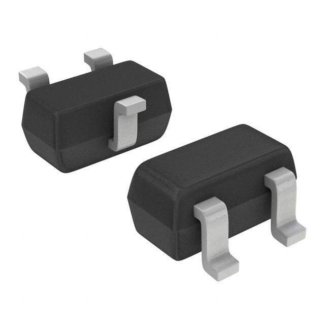
| 描述 | DIODE SCHOTTKY 30V 200MA SC89肖特基二极管与整流器 30V 225mW Dual Common Cathode |
| 产品分类 | 二极管,整流器 - 阵列分离式半导体 |
| 品牌 | ON Semiconductor |
| 产品手册 | |
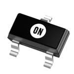
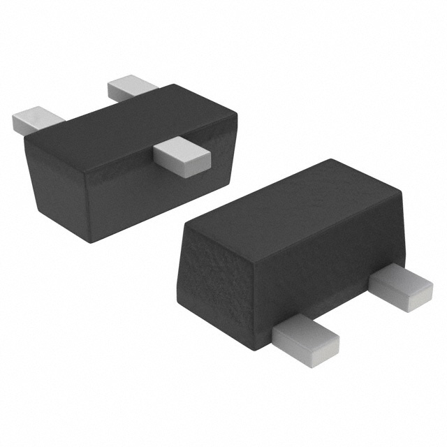
| 产品图片 |
|
| rohs | 符合RoHS无铅 / 符合限制有害物质指令(RoHS)规范要求 |
| 产品系列 | 二极管与整流器,肖特基二极管与整流器,ON Semiconductor BAT54CXV3T1G- |
| 数据手册 | |
| 产品型号 | BAT54CXV3T1G |
| PCN设计/规格 | |
| 不同If时的电压-正向(Vf) | 800mV @ 100mA |
| 不同 Vr时的电流-反向漏电流 | 2µA @ 25V |
| 二极管类型 | |
| 二极管配置 | 1 对共阴极 |
| 产品 | Schottky Diodes |
| 产品种类 | 肖特基二极管与整流器 |
| 供应商器件封装 | SC-89-3 |
| 其它名称 | BAT54CXV3T1GOSDKR |
| 包装 | Digi-Reel® |
| 反向恢复时间(trr) | 5ns |
| 商标 | ON Semiconductor |
| 安装类型 | 表面贴装 |
| 安装风格 | SMD/SMT |
| 封装 | Reel |
| 封装/外壳 | SC-89,SOT-490 |
| 封装/箱体 | SC-89 |
| 峰值反向电压 | 30 V |
| 工作温度范围 | - 55 C to + 125 C |
| 工厂包装数量 | 3000 |
| 恢复时间 | 5 ns |
| 技术 | Silicon |
| 最大反向漏泄电流 | 2 uA |
| 最大工作温度 | + 125 C |
| 最大浪涌电流 | 0.6 A |
| 最小工作温度 | - 55 C |
| 标准包装 | 1 |
| 正向电压下降 | 0.8 V at 0.1 A |
| 正向连续电流 | 0.2 A |
| 热阻 | 525°C/W Ja |
| 电压-DC反向(Vr)(最大值) | 30V |
| 电流-平均整流(Io)(每二极管) | 200mA(DC) |
| 系列 | BAT54CXV3 |
| 速度 | 小信号 =< 200mA(Io),任意速度 |
| 配置 | Dual Common Cathode |


- 商务部:美国ITC正式对集成电路等产品启动337调查
- 曝三星4nm工艺存在良率问题 高通将骁龙8 Gen1或转产台积电
- 太阳诱电将投资9.5亿元在常州建新厂生产MLCC 预计2023年完工
- 英特尔发布欧洲新工厂建设计划 深化IDM 2.0 战略
- 台积电先进制程称霸业界 有大客户加持明年业绩稳了
- 达到5530亿美元!SIA预计今年全球半导体销售额将创下新高
- 英特尔拟将自动驾驶子公司Mobileye上市 估值或超500亿美元
- 三星加码芯片和SET,合并消费电子和移动部门,撤换高东真等 CEO
- 三星电子宣布重大人事变动 还合并消费电子和移动部门
- 海关总署:前11个月进口集成电路产品价值2.52万亿元 增长14.8%

PDF Datasheet 数据手册内容提取
BAT54CXV3 Dual Series Schottky Barrier Diodes These Schottky barrier diodes are designed for high speed switching applications, circuit protection, and voltage clamping. Extremely low forward voltage reduces conduction loss. Miniature surface mount www.onsemi.com package is excellent for hand held and portable applications where space is limited. 30 VOLT Features • DUAL COMMON CATHODE Extremely Fast Switching Speed • Low Forward Voltage − 0.35 V (Typ) @ I = 10 mAdc SCHOTTKY BARRIER DIODES F • These Devices are Pb−Free, Halogen Free/BFR Free and are RoHS Compliant 3 2 1 MAXIMUM RATINGS (TJ = 125°C unless otherwise noted) SC−89 Rating Symbol Value Unit CASE 463C STYLE 3 Reverse Voltage VR 30 V Forward Power Dissipation PF @ TA = 25°C 240 mW 1 2 Derate above 25°C 1.9 mW/°C ANODE ANODE Forward Current (DC) IF 200 Max mA 3 CATHODE Non−Repetitive Peak Forward IFSM 600 mA Current, tp < 10 msec Repetitive Peak Forward Current IFRM 300 mA MARKING DIAGRAM Pulse Wave = 1 sec, Duty Cycle = 66% Junction Temperature TJ −55 to 125 °C 5CM(cid:2) (cid:2) Storage Temperature Range Tstg −55 to +150 °C 1 Thermal Resistance, R(cid:2)JA 525 °C/W Junction−to−Ambient (Note 1) 5C = Device Code Stresses exceeding those listed in the Maximum Ratings table may damage the M = Date Code device. If any of these limits are exceeded, device functionality should not be (cid:2) = Pb−Free Package assumed, damage may occur and reliability may be affected. (Note: Microdot may be in either location) 1. FR−4 board with minimum mounting pad. ORDERING INFORMATION Device Package Shipping† BAT54CXV3T1G SC−89 3000 / Tape & Reel (Pb−Free) †For information on tape and reel specifications, including part orientation and tape sizes, please refer to our Tape and Reel Packaging Specifications Brochure, BRD8011/D. © Semiconductor Components Industries, LLC, 2014 1 Publication Order Number: November, 2014 − Rev. 3 BAT54CXV3/D
BAT54CXV3 ELECTRICAL CHARACTERISTICS (TA = 25°C unless otherwise noted) (EACH DIODE) Characteristic Symbol Min Typ Max Unit Reverse Breakdown Voltage V(BR)R 30 − − V (IR = 10 (cid:3)A) Total Capacitance CT − 7.6 10 pF (VR = 1.0 V, f = 1.0 MHz) Reverse Leakage IR − 0.5 2.0 (cid:3)Adc (VR = 25 V) Forward Voltage VF V (IF = 0.1 mA) − 0.22 0.24 (IF = 1.0 mA) − 0.29 0.32 (IF = 10 mA) − 0.35 0.40 (IF = 30 mA) − 0.41 0.50 (IF = 100 mA) − 0.52 0.80 Reverse Recovery Time trr − − 5.0 ns (IF = IR = 10 mAdc, IR(REC) = 1.0 mAdc, Figure 1) Product parametric performance is indicated in the Electrical Characteristics for the listed test conditions, unless otherwise noted. Product performance may not be indicated by the Electrical Characteristics if operated under different conditions. 820 (cid:4) +10 V 120 k0 (cid:3)H IF 0.1 (cid:3)F tr tp T IF 0.1 (cid:3)F 10% trr T DUT 50 (cid:4) OUTPUT 50 (cid:4) INPUT 90% PULSE SAMPLING iR(REC) = 1 mA GENERATOR OSCILLOSCOPE VR IR OUTPUT PULSE INPUT SIGNAL (IF = IR = 10 mA; measured at iR(REC) = 1 mA) Notes: 1. A 2.0 k(cid:4) variable resistor adjusted for a Forward Current (IF) of 10 mA. Notes: 2. Input pulse is adjusted so IR(peak) is equal to 10 mA. Notes: 3. tp » trr Figure 1. Recovery Time Equivalent Test Circuit www.onsemi.com 2
BAT54CXV3 100 125°C A) m 85°C T ( N 10 E R R U C 150°C D R A 1.0 W R O , FF 25°C −40°C −55°C I 0.1 0.0 0.1 0.2 0.3 0.4 0.5 0.6 VF, FORWARD VOLTAGE (VOLTS) Figure 2. Forward Voltage 1000 TA = 150°C A) 100 (cid:3)T ( TA = 125°C N E 10 R R U C 1.0 E TA = 85°C S R E 0.1 V E R I, R 0.01 TA = 25°C 0.001 0 5 10 15 20 25 30 VR, REVERSE VOLTAGE (VOLTS) Figure 3. Leakage Current 14 F) 12 p E ( C 10 N A T CI 8 A P A 6 C L A T 4 O T , T 2 C 0 0 5 10 15 20 25 30 VR, REVERSE VOLTAGE (VOLTS) Figure 4. Total Capacitance www.onsemi.com 3
BAT54CXV3 PACKAGE DIMENSIONS SC−89, 3−LEAD CASE 463C−03 ISSUE C A −X− NOTES: 1. DIMENSIONING AND TOLERANCING PER ANSI Y14.5M, 1982. 2. CONTROLLING DIMENSION: MILLIMETERS 3. MAXIMUM LEAD THICKNESS INCLUDES LEAD 3 FINISH THICKNESS. MINIMUM LEAD THICKNESS B −Y− S IS THE MINIMUM THICKNESS OF BASE 1 2 MATERIAL. K 4. 463C−01 OBSOLETE, NEW STANDARD 463C−02. MILLIMETERS INCHES G DIM MIN NOM MAX MIN NOM MAX 2 PL A 1.50 1.60 1.70 0.059 0.063 0.067 D 3 PL B 0.75 0.85 0.95 0.030 0.034 0.040 C 0.60 0.70 0.80 0.024 0.028 0.031 0.08 (0.003) M X Y D 0.23 0.28 0.33 0.009 0.011 0.013 G 0.50 BSC 0.020 BSC H 0.53 REF 0.021 REF J 0.10 0.15 0.20 0.004 0.006 0.008 K 0.30 0.40 0.50 0.012 0.016 0.020 L 1.10 REF 0.043 REF M −−− −−− 10 _ −−− −−− 10 _ M N N −−− −−− 10 _ −−− −−− 10 _ J S 1.50 1.60 1.70 0.059 0.063 0.067 C STYLE 3: PIN 1.ANODE −T− SEATING 2.ANODE PLANE 3.CATHODE SOLDERING FOOTPRINT* 0.53 0.020 1.10 0.53 0.043 0.020 0.50 0.020 *For additional information on our Pb−Free strategy and soldering details, please download the ON Semiconductor Soldering and Mounting Techniques Reference Manual, SOLDERRM/D. ON Semiconductor and the are registered trademarks of Semiconductor Components Industries, LLC (SCILLC) or its subsidiaries in the United States and/or other countries. SCILLC owns the rights to a number of patents, trademarks, copyrights, trade secrets, and other intellectual property. A listing of SCILLC’s product/patent coverage may be accessed at www.onsemi.com/site/pdf/Patent−Marking.pdf. SCILLC reserves the right to make changes without further notice to any products herein. SCILLC makes no warranty, representation or guarantee regarding the suitability of its products for any particular purpose, nor does SCILLC assume any liability arising out of the application or use of any product or circuit, and specifically disclaims any and all liability, including without limitation special, consequential or incidental damages. “Typical” parameters which may be provided in SCILLC data sheets and/or specifications can and do vary in different applications and actual performance may vary over time. All operating parameters, including “Typicals” must be validated for each customer application by customer’s technical experts. SCILLC does not convey any license under its patent rights nor the rights of others. SCILLC products are not designed, intended, or authorized for use as components in systems intended for surgical implant into the body, or other applications intended to support or sustain life, or for any other application in which the failure of the SCILLC product could create a situation where personal injury or death may occur. Should Buyer purchase or use SCILLC products for any such unintended or unauthorized application, Buyer shall indemnify and hold SCILLC and its officers, employees, subsidiaries, affiliates, and distributors harmless against all claims, costs, damages, and expenses, and reasonable attorney fees arising out of, directly or indirectly, any claim of personal injury or death associated with such unintended or unauthorized use, even if such claim alleges that SCILLC was negligent regarding the design or manufacture of the part. SCILLC is an Equal Opportunity/Affirmative Action Employer. This literature is subject to all applicable copyright laws and is not for resale in any manner. PUBLICATION ORDERING INFORMATION LITERATURE FULFILLMENT: N. American Technical Support: 800−282−9855 Toll Free ON Semiconductor Website: www.onsemi.com Literature Distribution Center for ON Semiconductor USA/Canada P.O. Box 5163, Denver, Colorado 80217 USA Europe, Middle East and Africa Technical Support: Order Literature: http://www.onsemi.com/orderlit Phone: 303−675−2175 or 800−344−3860 Toll Free USA/Canada Phone: 421 33 790 2910 Fax: 303−675−2176 or 800−344−3867 Toll Free USA/Canada Japan Customer Focus Center For additional information, please contact your local Email: orderlit@onsemi.com Phone: 81−3−5817−1050 Sales Representative www.onsemi.com BAT54CXV3/D 4