ICGOO在线商城 > BA2115F-E2
 Datasheet下载
- 型号: BA2115F-E2
- 制造商: ROHM Semiconductor
- 库位|库存: xxxx|xxxx
- 要求:
| 数量阶梯 | 香港交货 | 国内含税 |
| +xxxx | $xxxx | ¥xxxx |
查看当月历史价格
查看今年历史价格
BA2115F-E2产品简介:
ICGOO电子元器件商城为您提供BA2115F-E2由ROHM Semiconductor设计生产,在icgoo商城现货销售,并且可以通过原厂、代理商等渠道进行代购。 提供BA2115F-E2价格参考¥2.34-¥5.67以及ROHM SemiconductorBA2115F-E2封装/规格参数等产品信息。 你可以下载BA2115F-E2参考资料、Datasheet数据手册功能说明书, 资料中有BA2115F-E2详细功能的应用电路图电压和使用方法及教程。
| 参数 | 数值 |
| -3db带宽 | - |
| 产品目录 | 集成电路 (IC)半导体 |
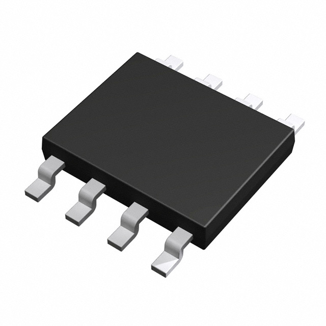
| 描述 | IC OPAMP GP 12MHZ 8SOP运算放大器 - 运放 1-7V 2 CHANNELS 150nA 3.5mA |
| 产品分类 | Linear - Amplifiers - Instrumentation, OP Amps, Buffer Amps集成电路 - IC |
| 品牌 | Rohm Semiconductor |
| 产品手册 | |
| 产品图片 |
|
| rohs | 符合RoHS无铅 / 符合限制有害物质指令(RoHS)规范要求 |
| 产品系列 | 放大器 IC,运算放大器 - 运放,ROHM Semiconductor BA2115F-E2- |
| 数据手册 | |
| 产品型号 | BA2115F-E2 |
| 产品目录页面 | |
| 产品种类 | 运算放大器 - 运放 |
| 供应商器件封装 | 8-SOP |
| 共模抑制比—最小值 | 60 dB |
| 关闭 | No Shutdown |
| 其它名称 | BA2115F-E2TR |
| 包装 | 带卷 (TR) |
| 压摆率 | 4 V/µs |
| 双重电源电压 | +/- 3 V, +/- 5 V |
| 商标 | ROHM Semiconductor |
| 增益带宽生成 | 12 MHz |
| 增益带宽积 | 12MHz |
| 安装类型 | 表面贴装 |
| 安装风格 | SMD/SMT |
| 封装 | Reel |
| 封装/外壳 | 8-SOIC(0.173",4.40mm 宽) |
| 封装/箱体 | SOP-8 |
| 工作温度 | -40°C ~ 85°C |
| 工作电源电压 | 2 V to 14 V, +/- 1 V to +/- 7 V |
| 工厂包装数量 | 2500 |
| 技术 | Bipolar |
| 放大器类型 | 通用 |
| 最大双重电源电压 | +/- 7 V |
| 最大工作温度 | + 85 C |
| 最小双重电源电压 | +/- 1 V |
| 最小工作温度 | - 40 C |
| 标准包装 | 2,500 |
| 电压-电源,单/双 (±) | 2 V ~ 14 V, ±1 V ~ 7 V |
| 电压-输入失调 | 1mV |
| 电流-电源 | 3.5mA |
| 电流-输入偏置 | 150nA |
| 电流-输出/通道 | 10mA |
| 电源电流 | 5 mA |
| 电路数 | 2 |
| 转换速度 | 4 V/us |
| 输入偏压电流—最大 | 500 nA |
| 输入补偿电压 | 6 mV |
| 输出电流 | 10 mA |
| 输出类型 | - |
| 通道数量 | 2 Channel |


- 商务部:美国ITC正式对集成电路等产品启动337调查
- 曝三星4nm工艺存在良率问题 高通将骁龙8 Gen1或转产台积电
- 太阳诱电将投资9.5亿元在常州建新厂生产MLCC 预计2023年完工
- 英特尔发布欧洲新工厂建设计划 深化IDM 2.0 战略
- 台积电先进制程称霸业界 有大客户加持明年业绩稳了
- 达到5530亿美元!SIA预计今年全球半导体销售额将创下新高
- 英特尔拟将自动驾驶子公司Mobileye上市 估值或超500亿美元
- 三星加码芯片和SET,合并消费电子和移动部门,撤换高东真等 CEO
- 三星电子宣布重大人事变动 还合并消费电子和移动部门
- 海关总署:前11个月进口集成电路产品价值2.52万亿元 增长14.8%


PDF Datasheet 数据手册内容提取
Datasheet Operational Amplifiers Lo w Noise Operational Amplifiers BA2107G BA2115xxx General Description Key Specification The BA2107/BA2115 are single and dual operational Wide Operating Supply Voltage amplifier with high gain and high slew rate(4v/µs). (split supply): ±1.0V to ±7.0V The BA2107/BA2115 have good performance of input Operating Temperature Range: -40°C to +85°C referred noise voltage(7nV/ Hz) and total harmonic Slew Rate: 4V/µs(Typ) distortion(0.008%). These are suitable for Audio Total Harmonic Distortion : 0.008%(Typ) applications. Input Referred Noise Voltage : 7nV/ Hz(Typ) Features Packages W(Typ)xD(Typ) xH(Max) High Voltage Gain SSOP5 2.90mm x 2.80mm x 1.25mm Low Input Referred Noise Voltage SOP8 5.00mm x 6.20mm x 1.71mm Low Total Harmonic Distortion SOP-J8 4.90mm x 6.00mm x 1.65mm Wide Operating Supply Voltage MSOP8 2.90mm x 4.00mm x 0.90mm Application Audio Application Potable Equipment Consumer Electronics Simplified Schematic VVCCCC --ININ VOOUUTT ++ININ VVEEEE Figure 1. Simplified Schematic ○Product structure:Silicon monolithic integrated circuit ○This product is not designed protection against radioactive rays. www.rohm.com TSZ02201-0RAR0G200090-1-2 © 2012 ROHM Co., Ltd. All rights reserved. 1/31 11.Nov.2014 Rev.002 TSZ22111・14・00
B A2107G BA2115xxx Datasheet Pin Configuration SSOP5 +IN 1 5 VCC Pin No. Pin Name 1 +IN1 + VEE 2 - 2 VEE -IN 3 4 OUT 3 -IN1 4 OUT 5 VCC SOP8, SOP-J8, MSOP8 Pin No. Pin Name OUT1 1 8 VCC 1 OUT1 2 -IN1 -IN1 2 CH1 7 OUT2 - + 3 +IN1 4 VEE 3 6 -IN2 +IN1 CH2 5 +IN2 + - VEE 4 5 +IN2 6 -IN2 7 OUT2 8 VCC Package SSOP5 SOP8 SOP-J8 MSOP8 BA2107G BA2115F BA2115FJ BA2115FVM Ordering Information B A 2 1 x x x x x - x x Part Number Package Packaging and forming specification BA2107G G : SSOP5 E2: Embossed tape and reel BA2115xxx F : SOP8 (SOP8/SOP-J8) FJ : SOP-J8 TR: Embossed tape and reel FVM : MSOP8 (SSOP5/MSOP8) Line-up Operating Operating Supply Supply Slew Orderable Temperature Voltage Current Rate Package Part Number Range (split supply) (Typ) (Typ) SSOP5 Reel of 3000 BA2107G-TR SOP8 Reel of 2500 BA2115F-E2 -40°C to +85°C ±1.0V to ±7.0V 3.5mA 4V/µs SOP-J8 Reel of 2500 BA2115FJ-E2 MSOP8 Reel of 3000 BA2115FVM-TR www.rohm.com TSZ02201-0RAR0G200090-1-2 © 2012 ROHM Co., Ltd. All rights reserved. 2/31 11.Nov.2014 Rev.002 TSZ22111・15・00
B A2107G BA2115xxx Datasheet Absolute Maximum Ratings (T =25℃) A ○BA2107, BA2115 Parameter Symbol Ratings Unit Supply Voltage VCC-VEE +14 V SSOP5 0.67(Note 1,4) SOP8 0.78(Note 2,4) Power Dissipation P W D SOP-J8 0.67(Note 1,4) MSOP8 0.59(Note 3,4) Differential Input Voltage (Note 5) C +14 V Input Common-mode Voltage Range V (VEE-0.3) to (VEE+14) V ICM Input Current(Note 6) I -10 mA I Operating Supply Voltage V 2 to 14(±1 to ±7) V opr Operating Temperature T -40 to +85 ℃ opr Storage Temperature T -55 to 150 ℃ stg Maximum Junction Temperature T +150 ℃ Jmax (Note 1) To use at temperature above TA=25℃ reduce 5.4mW/℃ (Note 2) To use at temperature above TA=25℃ reduce 6.2mW/℃ (Note 3) To use at temperature above TA=25℃ reduce 4.8mW/℃ (Note 4) Mounted on a FR4 glass epoxy PCB 70mm×70mm×1.6mm (copper foil area less than 3%). (Note 5) The voltage difference between inverting input and non-inverting input is the differential input voltage. Then input terminal voltage is set to more than VEE. (Note 6) An excessive input current will flow when input voltages of more than VCC+0.6V or less than VEE-0.6V are applied. The input current can be set to less than the rated current by adding a limiting resistor. Caution: Operating the IC over the absolute maximum ratings may damage the IC. In addition, it is impossible to predict all destructive situations such as short-circuit modes, open circuit modes, etc. Therefore, it is important to consider circuit protection measures, like adding a fuse, in case the IC is operated in a special mode exceeding the absolute maximum ratings. www.rohm.com TSZ02201-0RAR0G200090-1-2 © 2012 ROHM Co., Ltd. All rights reserved. 3/31 11.Nov.2014 Rev.002 TSZ22111・15・00
B A2107G BA2115xxx Datasheet Electrical Characteristics ○BA2107 (Unless otherwise specified VCC=+2.5V, VEE=-2.5V, T =25℃) A Limits Parameter Symbol Unit Condition Min Typ Max Input Offset Voltage (Note 7) V - 1 6 mV VOUT=0V, V =0V IO ICM Input Offset Current (Note 7) I - 2 200 nA VOUT=0V, V =0V IO ICM Input Bias Current (Note 8) I - 150 400 nA VOUT=0V, V =0V B ICM Supply Current I - 1.8 3.0 mA Av=0dB, R =∞, +IN=0V CC L 4.5 4.8 - R ≧2.5kΩ, V =VCC-0.5V L OHmin R ≧10kΩ, VCC=12V, VEE=0V - 11.6 - L Maximum Output Voltage(High) VOH V VRL=6V, VOH=VCC-0.4V R ≧10kΩ, VCC=16V, VEE=0V - 15.5 - L V =8V, V =VCC-0.5V RL OH 0.5 0.2 - R ≧2.5kΩ, V =VEE+0.5V L OLmin R ≧10kΩ, VCC=12V, VEE=0V - 0.4 - L Maximum Output Voltage(Low) VOL V VRL=6V, VOL=VEE+0.4V R ≧10kΩ, VCC=16V, VEE=0V - 0.5 - L V =8V, V =VEE+0.5V RL OL Output Source Current I - 1.4 - mA - SOURCE Output Sink Current I - 90 - mA - SINK R ≧10kΩ, VOUT=2.5±2V Large Signal Voltage Gain Av 60 80 - dB L V =2.5V ICM Input Common-mode Voltage Range V ±1.5 - - V (VEE+1.0V) - (VCC-1.0V) ICM Common-mode Rejection Ratio CMRR 60 74 - dB V =-1.5V to +1.5V ICM Power Supply Rejection Ratio PSRR 60 80 - dB VEE=0V, VCC=2V to 16V Slew Rate SR - 4 - V/μs Av=0dB, +IN=2V P-P Gain Bandwidth Product GBW - 12 - MHz f=10kHz Unity Gain Frequency f - 3.4 - MHz 0dB cross frequency T - 7 - nV/ Hz RS=600Ω, DIN-AUDIO Input Referred Noise Voltage V N - 0.9 - μVrms R =600Ω, DIN-AUDIO S Total Harmonic Distortion THD+N - 0.008 - % Av=20dB, f=1kHz, DIN-AUDIO (Note 7) Absolute value (Note 8) Current direction: Since first input stage is composed with PNP transistor, input bias current flows out from IC. www.rohm.com TSZ02201-0RAR0G200090-1-2 © 2012 ROHM Co., Ltd. All rights reserved. 4/31 11.Nov.2014 Rev.002 TSZ22111・15・00
B A2107G BA2115xxx Datasheet ○BA2115 (Unless otherwise specified VCC=+2.5V, VEE=-2.5V, T =25℃) A Limits Unit Parameter Symbol Condition Min Typ Max Input Offset Voltage (Note 9) V - 1 6 mV VOUT=0V, V =0V IO ICM Input Offset Current (Note 9) I - 2 200 nA VOUT=0V, V =0V IO ICM Input Bias Current (Note 10) I - 150 400 nA VOUT=0V, V =0V B ICM Av=0dB, R =∞, All Op-Amps Supply Current I - 3.5 5 mA L CC +IN=0V 4.5 4.8 - R ≧2.5kΩ, V =VCC-0.5V L OHmin R ≧10kΩ, VCC=12V, VEE=0V - 11.6 - L Maximum Output Voltage(High) VOH V VRL=6V, VOH=VCC-0.4V R ≧10kΩ, VCC=16V, VEE=0V - 15.5 - L V =8V, V =VCC-0.5V RL OH 0.5 0.2 - R ≧2.5kΩ, V =VEE+0.5V L OLmin R ≧10kΩ, VCC=12V, VEE=0V - 0.4 - L Maximum Output Voltage(Low) VOL V VRL=6V, VOL=VEE+0.4V R ≧10kΩ, VCC=16V, VEE=0V - 0.5 - L V =8V, V =VEE+0.5V RL OL Output Source Current I - 1.4 - mA - SOURCE Output Sink Current I - 90 - mA - SINK R ≧10kΩ, VOUT=±2V Large Signal Voltage Gain A 60 80 - dB L V V =0V ICM Input Common-mode Voltage Range V ±1.5 - - V (VEE+1.0V) - (VCC-1.0V) ICM Common-mode Rejection Ratio CMRR 60 74 - dB V =-1.5V to +1.5V ICM Power Supply Rejection Ratio PSRR 60 80 - dB VEE=0V, VCC=2V to 14V Slew Rate SR - 4 - V/μs Av=0dB, +IN=2V PP Gain Bandwidth Product GBW - 12 - MHz f=10kHz Unity Gain Frequency f - 3.4 - MHz 0dB cross frequency T - 7 - nV/ Hz RS=600Ω, DIN-AUDIO Input Referred Noise Voltage V N - 0.9 - μVrms R =600Ω, DIN-AUDIO S Total Harmonic Distortion THD+N - 0.008 - % Av=20dB, f=1kHz, DIN-AUDIO Channel Separation CS - 100 - dB Av=40dB (Note 9) Absolute value (Note 10) Current direction: Since first input stage is composed with PNP transistor, input bias current flows out from IC. www.rohm.com TSZ02201-0RAR0G200090-1-2 © 2012 ROHM Co., Ltd. All rights reserved. 5/31 11.Nov.2014 Rev.002 TSZ22111・15・00
B A2107G BA2115xxx Datasheet Description of Electrical Characteristics Described below are descriptions of the relevant electrical terms used in this datasheet. Items and symbols used are also shown. Note that item name and symbol and their meaning may differ from those on another manufacturer’s document or general document. 1. Absolute maximum ratings Absolute maximum rating items indicate the condition which must not be exceeded. Application of voltage in excess of absolute maximum rating or use out of absolute maximum rated temperature environment may cause deterioration of characteristics. (1) Supply Voltage (VCC / VEE) Indicates the maximum voltage that can be applied between the positive power supply terminal and negative power supply terminal without deterioration or destruction of characteristics of internal circuit. (2) Differential Input Voltage (V ) ID Indicates the maximum voltage that can be applied between non-inverting and inverting terminals without damaging the IC. (3) Input Common-mode Voltage Range (V ) ICM Indicates the maximum voltage that can be applied to the non-inverting and inverting terminals without deterioration or destruction of electrical characteristics. Input common-mode voltage range of the maximum ratings does not assure normal operation of IC. For normal operation, use the IC within the input common-mode voltage range characteristics. (4) Power dissipation (P ) D Indicates the power that can be consumed by the IC when mounted on a specific board at the ambient temperature 25℃ (normal temperature). As for package product, Pd is determined by the temperature that can be permitted by the IC in the package (maximum junction temperature) and the thermal resistance of the package. 2. Electrical characteristics (1) Input Offset Voltage (V ) IO Indicates the voltage difference between non-inverting terminal and inverting terminals. It can be translated into the input voltage difference required for setting the output voltage at 0 V. (2) Input Offset Current (I ) IO Indicates the difference of input bias current between the non-inverting and inverting terminals. (3) Input Bias Current (I ) B Indicates the current that flows into or out of the input terminal. It is defined by the average of input bias currents at the non-inverting and inverting terminals. (4) Supply Current (I ) CC Indicates the current that flows within the IC under specified no-load conditions. (5) Maximum Output Voltage(High) / Maximum Output Voltage(Low) (VOH/VOL) Indicates the voltage range of the output under specified load condition. It is typically divided into maximum output voltage High and low. Maximum output voltage high indicates the upper limit of output voltage. Maximum output voltage low indicates the lower limit. (6) Output Source Current/ Output Sink Current (I / I ) source sink The maximum current that can be output from the IC under specific output conditions. The output source current indicates the current flowing out from the IC, and the output sink current indicates the current flowing into the IC. indicates the current flowing out from the IC, and the output sink current indicates the current flowing into the IC. (7) Large Signal Voltage Gain (Av) Indicates the amplifying rate (gain) of output voltage against the voltage difference between non-inverting terminal and inverting terminal. It is normally the amplifying rate (gain) with reference to DC voltage. Av = (Output voltage) / (Differential Input voltage) (8) Input Common-mode Voltage Range (V ) ICM Indicates the input voltage range where IC normally operates. (9) Common-mode Rejection Ratio (CMRR) Indicates the ratio of fluctuation of input offset voltage when the input common mode voltage is changed. It is normally the fluctuation of DC. CMRR = (Change of Input common-mode voltage)/(Input offset fluctuation) www.rohm.com TSZ02201-0RAR0G200090-1-2 © 2012 ROHM Co., Ltd. All rights reserved. 6/31 11.Nov.2014 Rev.002 TSZ22111・15・00
B A2107G BA2115xxx Datasheet (10) Power Supply Rejection Ratio (PSRR) Indicates the ratio of fluctuation of input offset voltage when supply voltage is changed. It is normally the fluctuation of DC. PSRR= (Change of power supply voltage)/(Input offset fluctuation) (11) Slew Rate (SR) Indicates the ratio of the change in output voltage with time when a step input signal is applied. (12) Gain Bandwidth (GBW) The product of the open-loop voltage gain and the frequency at which the voltage gain decreases 6dB/octave. (13) Unity gain frequency (f ) T Indicates a frequency where the voltage gain of operational amplifier is 1. (14) Input Referred Noise Voltage (V ) N Indicates a noise voltage generated inside the operational amplifier equivalent by ideal voltage source connected in series with input terminal. (15) Total harmonic distortion + Noise (THD+N) Indicates the fluctuation of input offset voltage or that of output voltage with reference to the change of output voltage of driven channel. (16) Channel Separation (CS) Indicates the fluctuation in the output voltage of the driven channel with reference to the change of output voltage of the channel which is not driven. www.rohm.com TSZ02201-0RAR0G200090-1-2 © 2012 ROHM Co., Ltd. All rights reserved. 7/31 11.Nov.2014 Rev.002 TSZ22111・15・00
B A2107G BA2115xxx Datasheet Typical Performance Curves ○BA2107 1.0 4 W] 0.8 mA] . 3 N [ BA2107G T [ -40℃ O 0.6 N TI E 25℃ A R P R 2 SI U DIS 0.4 Y C R PL 85℃ E P W U 1 O 0.2 S P 0.0 0 0 25 50 75 85 100 125 0 5 10 15 AMBIENT TEMPERATURE [℃] SUPPLY VOLTAGE [V] Figure 2. Figure 3. Derating Curve Supply Current - Supply Voltage 4 3 2 VOH mA] 3 V] NT [ 5.0V 14.0V AGE [ 1 E T RR 2 OL 0 Y CU UT V PL TP -1 UP 1 2.0V OU S VOL -2 0 -3 -50 -25 0 25 50 75 100 0.1 1 10 100 1000 10000 AMBIENT TEMPERATURE [℃] LOLOADA DR ERSEISSITSATANNCCEE [k [ΩkΩ] ] Figure 5. Figure 4. Output Voltage - Load Resistance Supply Current - Ambient Temperature (VCC/VEE=+2.5V/-2.5V) (*)The above data is measurement value of typical sample, it is not guaranteed. www.rohm.com TSZ02201-0RAR0G200090-1-2 © 2012 ROHM Co., Ltd. All rights reserved. 8/31 11.Nov.2014 Rev.002 TSZ22111・15・00
B A2107G BA2115xxx Datasheet ○BA2107 10 10 6 6 VOH VOH V] V] E [ E [ G G A 2 A 2 T T L L O O V V T -2 T -2 U U P P UT UT O -6 VOL O -6 VOL -10 -10 ±1 ±2 ±3 ±4 ±5 ±6 ±7 ±8 -50 -25 0 25 50 75 100 SUPPLY VOLTAGE [V] AMBIENT TEMPERATURE [℃] Figure 6. Figure 7. Output Voltage - Supply Voltage Output Voltage - Ambient Temperature (R =10kΩ) L (VCC/VEE=+7.0V/-7.0V, RL=10kΩ) 3.0 0 2.5 -0.5 V] V] E [ 2.0 VOH E [ -1 G G A A T T OL 1.5 OL -1.5 V V T T VOL U U P 1.0 P -2 T T U U O O 0.5 -2.5 0.0 -3 0.0 0.4 0.8 1.2 1.6 2.0 0 2 4 6 8 10 OUTPUT SOURCE CURRENT [mA] OUTPUT SINK CURRENT [mA] Figure 8. Figure 9. Output Voltage - Output Source Current Output Voltage - Output Sink Current (VCC/VEE=+2.5V/-2.5V) (VCC/VEE=+2.5V/-2.5V) (*)The above data is measurement value of typical sample, it is not guaranteed. www.rohm.com TSZ02201-0RAR0G200090-1-2 © 2012 ROHM Co., Ltd. All rights reserved. 9/31 11.Nov.2014 Rev.002 TSZ22111・15・00
B A2107G BA2115xxx Datasheet ○BA2107 6 3 V] 4 V] 2 m m E [ E [ G 2 G 1 ±2.5V ±7.0V A A T T L L O O V 0 V 0 ET ET ±1.0V S S FF -2 FF -1 O O T T U U P -4 P -2 N N I I -6 -3 ±1 ±2 ±3 ±4 ±5 ±6 ±7 ±8 -50 -25 0 25 50 75 100 SUPPLY VOLTAGE [V] AMBIENT TEMPERATURE [°C] Figure 10. Figure 11. Input Offset Voltage - Supply Voltage Input Offset Voltage - Ambient Temperature (VICM=0V, VOUT=0V) (VICM=0V, VOUT=0V) 250 250 T [nA] 200 25℃ -40℃ T [nA] . 200 ±1.0V± 2.5V N N E E RR 150 RR 150 ±7.0V U 85℃ U C C S S A 100 A 100 BI BI T T U U P P N 50 N 50 I I 0 0 ±1 ±2 ±3 ±4 ±5 ±6 ±7 ±8 -50 -25 0 25 50 75 100 SUPPLY VOLTAGE [V] AMBIENT TEMPERATURE [°C] Figure 12. Figure 13. Input Bias Current - Supply Voltage Input Bias Current - Ambient Temperature (VICM=0V, VOUT=0V) (VICM=0V, VOUT=0V) (*)The above data is measurement value of typical sample, it is not guaranteed. www.rohm.com TSZ02201-0RAR0G200090-1-2 © 2012 ROHM Co., Ltd. All rights reserved. 10/31 11.Nov.2014 Rev.002 TSZ22111・15・00
B A2107G BA2115xxx Datasheet ○BA2107 A] . 3400 A] 3400 NT [n 20 NT [n 20 ±1.0V E -40℃ 25℃ E RR 10 RR 10 U U OFFSET C -100 85℃ OFFSET C -100 ±2.5V ±7.0V PUT -20 PUT -20 IN -30 IN -30 -40 -40 ±1 ±2 ±3 ±4 ±5 ±6 ±7 ±8 -50 -25 0 25 50 75 100 SUPPLY VOLTAGE [V] AMBIENT TEMPERATURE [℃] Figure 14. Figure 15. Input Offset Current - Supply Voltage Input Offset Current - Ambient Temperature (VICM=0V, VOUT=0V) (VICM=0V, VOUT=0V) 6 150 V] 4 -40℃ dB] . 125 E [m 25℃ AIN [ TAG 2 85℃ E G 100 L G O A ET V 0 OLT 75 S V F L OF -2 NA 50 T G U SI NP -4 GE 25 I R A L -6 0 -2.5 -1.5 -0.5 0.5 1.5 2.5 -50 -25 0 25 50 75 100 COMMON MODE INPUT VOLTAGE [V] AMBIENT TEMPERATURE [°C] Figure 17. Figure 16. Large Signal Voltage Gain Input Offset Voltage - Ambient Temperature - Common Mode Input Voltage (VCC/VEE=+2.5V/-2.5V) (VCC/VEE=+2.5V/-2.5V, VOUT=0V) (*)The above data is measurement value of typical sample, it is not guaranteed. www.rohm.com TSZ02201-0RAR0G200090-1-2 © 2012 ROHM Co., Ltd. All rights reserved. 11/31 11.Nov.2014 Rev.002 TSZ22111・15・00
B A2107G BA2115xxx Datasheet ○BA2107 B]150 B] 150 d d O [ O[ TI125 ATI 125 TION RA100 CTION R 100 C E E J EJ.75 RE.75 E R LY OD 50 PP 50 M U MON 25 ER S 25 W M O O P C 0 0 -50 -25 0 25 50 75 100 -50 -25 0 25 50 75 100 AMBIENT TEMPERATURE [°C] AMBIENT TEMPERATURE [°C] Figure 18. Figure 19. Common Mode Rejection Ratio Power Supply Rejection Ratio - Ambient Temperature - Ambient Temperature (VCC/VEE=+2.5V/-2.5V) (VCC/VEE=+2.5V/-2.5V) 7 7 6 6 μs] 5 μs]5 H [V/ -40℃ 25℃ L [V/ -40℃ 25℃ L- 4 H-4 E E T T A 3 A3 85℃ R 85℃ R W W E E L 2 L2 S S 1 1 0 0 ±1 ±2 ±3 ±4 ±5 ±6 ±7 ±8 ±1 ±2 ±3 ±4 ±5 ±6 ±7 ±8 SUPPLY VOLTAGE[V] SUPPLY VOLTAGE [V] Figure 20. Figure 21. Slew Rate L-H - Supply Voltage Slew Rate H-L - Supply Voltage (*)The above data is measurement value of typical sample, it is not guaranteed. www.rohm.com TSZ02201-0RAR0G200090-1-2 © 2012 ROHM Co., Ltd. All rights reserved. 12/31 11.Nov.2014 Rev.002 TSZ22111・15・00
B A2107G BA2115xxx Datasheet ○BA2107 1 Hz] 40 %] √ N [ nV/ O E [ TI G 30 OR 0.1 TA T L S O DI V NIC 20kHz OISE 20 O M N R0.01 D A R H E L 1kHz FF 10 TA 20Hz RE TO T U P 0.001 N 0 I 0.01 0.1 1 10 1 10 100 1000 10000 OUTPUT VOLTAGE [Vrms] FREQUENCY [Hz] Figure 22. Figure 23. Total Harmonic Distortion - Output Voltage Equivalent Input Noise Voltage - Frequency (VCC/VEE=2.5V/-2.5V, RL=2kΩ (VCC/VEE=2.5V/-2.5V) 80kHz-LPF, T =25℃) A 50 0 Phase -30 40 B] . 30 Gain -60 eg] . GAIN [d 20 -90 HASE [d -120P 10 -150 0 -180 1.1E0+20 2 1 .E10+30 3 1 .E10+40 4 1 .E1+050 5 1 .E1+006 6 1 1.E0+7 07 FREQUENCY [Hz] Figure 24. Voltage Gain - Frequency (VCC/VEE=2.5V/-2.5V, Av=40dB, R =10kΩ) L (*)The above data is measurement value of typical sample, it is not guaranteed. www.rohm.com TSZ02201-0RAR0G200090-1-2 © 2012 ROHM Co., Ltd. All rights reserved. 13/31 11.Nov.2014 Rev.002 TSZ22111・15・00
B A2107G BA2115xxx Datasheet Typical Performance Curves ○BA2115 W] . 01..80 BA2115F 67 -40℃ N [ mA]. 5 ATIO 0.6 BA2115FJ NT [ 4 25℃ P E SI RR 85℃ DIS 0.4 CU 3 R Y WE BA2115FVM PL 2 O UP P 0.2 S 1 0.0 0 85 0 25 50 75 100 125 0 5 10 15 AMBIENT TEMPERATURE [℃] SUPPLY VOLTAGE [V] Figure 25. Figure 26. Derating Curve Supply Current - Supply Voltage 7 3 6 2 VOH ENT [mA] 45 14.0V TAGE [V] 1 R L 0 R O CU 3 5.0V T V Y U PPL 2 3.0V UTP -1 VOL U O S -2 1 -3 0 0.1 1 10 100 1000 10000 -50 -25 0 25 50 75 100 AMBIENT TEMPERATURE [℃] LOAD RESISTANCE [kΩ] Figure 28. Figure 27. Output Voltage - Load Resistance Supply Current - Ambient Temperature (VCC/VEE=+2.5V/-2.5V) (*)The above data is measurement value of typical sample, it is not guaranteed. www.rohm.com TSZ02201-0RAR0G200090-1-2 © 2012 ROHM Co., Ltd. All rights reserved. 14/31 11.Nov.2014 Rev.002 TSZ22111・15・00
B A2107G BA2115xxx Datasheet ○BA2115 10 10 8 8 6 VOH 6 VOH AGE [V] 24 AGE [V] 24 OLT 0 OLT 0 V V UT -2 UT -2 P P UT -4 UT -4 VOL O -6 VOL O -6 -8 -8 -10 -10 -50 -25 0 25 50 75 100 ±1 ±2 ±3 ±4 ±5 ±6 ±7 ±8 SUPPLY VOLTAGE [V] AMBIENT TEMPERATURE [℃] Figure 29. Figure 30. Maximum Output Voltage Maximum Output Voltage - Supply Voltage - Ambient Temperature (RL=10kΩ) (VCC/VEE=+7V/-7V, RL=10kΩ) 3.0 0.0 2.5 -0.5 V] A]. GE [ 2.0 T [m -1.0 A VOH N T E OL 1.5 RR -1.5 T V CU VOL U Y P 1.0 L -2.0 T P U P O U S 0.5 -2.5 0.0 -3.0 0.0 0.4 0.8 1.2 1.6 2.0 0 2 4 6 8 10 OUTPUT SOURCE CURRENT [mA] SUPPLY VOLTAGE [V] Figure 31. Figure 32. Maximum Output Voltage Maximum Output Voltage - Output Source Current - Output Sink Current (VCC/VEE=+2.5V/-2.5V) (VCC/VEE=+2.5V/-2.5V) (*)The above data is measurement value of typical sample, it is not guaranteed. www.rohm.com TSZ02201-0RAR0G200090-1-2 © 2012 ROHM Co., Ltd. All rights reserved. 15/31 11.Nov.2014 Rev.002 TSZ22111・15・00
B A2107G BA2115xxx Datasheet ○BA2115 6 3 V] 4 V] 2 m m E [ E [ TAG 2 TAG 1 OL OL ±7.0V ET V 0 ET V 0 FS FS OF -2 OF -1 ±1.5V T T ±2.5V NPU -4 NPU -2 I I -6 -3 ±1 ±2 ±3 ±4 ±5 ±6 ±7 ±8 -50 -25 0 25 50 75 100 SUPPLY VOLTAGE [V] AMBIENT TEMPERATURE [°C] Figure 33. Figure 34. Input Offset Voltage - Supply Voltage Input Offset Voltage - Ambient Temperature (VICM=0V, VOUT=0V) (VICM=0V, VOUT=0V) 250 250 nA] . . 200 25℃ -40℃ nA] . 200 ±1.5V ±2.5V T [ T [ N N E E R 150 R 150 R R U U ±7.0V C C AS 100 85℃ AS 100 BI BI T T U U P P N 50 N 50 I I 0 0 ±1 ±2 ±3 ±4 ±5 ±6 ±7 ±8 -50 -25 0 25 50 75 100 SUPPLY VOLTAGE [V] AMBIENT TEMPERATURE [°C] Figure 35. Figure 36. Input Bias Current - Supply Voltage Input Bias Current - Ambient Temperature (VICM=0V, VOUT=0V) (VICM=0V, VOUT=0V) (*)The above data is measurement value of typical sample, it is not guaranteed. www.rohm.com TSZ02201-0RAR0G200090-1-2 © 2012 ROHM Co., Ltd. All rights reserved. 16/31 11.Nov.2014 Rev.002 TSZ22111・15・00
B A2107G BA2115xxx Datasheet ○BA2115 nA] . 3400 nA] 3400 T [ 20 T [ 20 N N ±1.5V RRE 10 -40℃ 25℃ RRE 10 U U C FFSET C -100 85℃ OFFSET -100 ±2.5V ±7.0V O T -20 UT -20 U P P N N -30 I -30 I -40 -40 ±1 ±2 ±3 ±4 ±5 ±6 ±7 ±8 -50 -25 0 25 50 75 100 SUPPLY VOLTAGE [V] AMBIENT TEMPERATURE [℃] Figure 37. Figure 38. Input Offset Current - Supply Voltage Input Offset Current - Ambient Temperature (V =0V, VOUT=0V) (V =0V, VOUT=0V) ICM ICM 20 150 mV] 15 N [dB] . 125 E [ 10 GAI AG E 100 T 5 G L A O T SET V 0 85℃ L VOL 75 F -5 A OF 25℃ GN 50 NPUT -10 -40℃ GE SI 25 I -15 AR L 0 -20 -2.5 -2 -1.5 -1 -0.5 0 0.5 1 1.5 2 2.5 -50 -25 0 25 50 75 100 COMMON MODE INPUT VOLTAGE [V] AMBIENT TEMPERATURE [°C] Figure 39. Figure 40. Input Offset Voltage Large Signal Voltage Gain - Common Mode Input Voltage - Ambient Temperature (VCC/VEE=+2.5V/-2.5V, VOUT=0V) (VCC/VEE=+2.5V/-2.5V) (*)The above data is measurement value of typical sample, it is not guaranteed. www.rohm.com TSZ02201-0RAR0G200090-1-2 © 2012 ROHM Co., Ltd. All rights reserved. 17/31 11.Nov.2014 Rev.002 TSZ22111・15・00
B A2107G BA2115xxx Datasheet ○BA2115 dB] . 150 B] . 150 ATIO [ 125 TIO [d 125 R A ON 100 N R 100 O CTI TI E C EJ 75 JE 75 DE R 50 LY RE 50 O P M P N SU O 25 R 25 M E M W O O C 0 P 0 -50 -25 0 25 50 75 100 -50 -25 0 25 50 75 100 AMBIENT TEMPERATURE [°C] AMBIENT TEMPERATURE [°C] Figure 41. Figure 42. Common Mode Rejection Ratio Power Supply Rejection Ratio - Ambient Temperature - Ambient Temperature (VCC/VEE=+2.5V/-2.5V) (VCC/VEE=+2.5V/-2.5V) 7 7 6 6 s] s] -40℃ 25℃ H [V/μ 5 -40℃ L [V/μ 5 L- 4 H- 4 RATE 3 85℃ 25℃ RATE 3 85℃ W W SLE 2 SLE 2 1 1 0 0 ±1 ±2 ±3 ±4 ±5 ±6 ±7 ±8 ±1 ±2 ±3 ±4 ±5 ±6 ±7 ±8 SUPPLY VOLTAGE[V] SUPPLY VOLTAGE [V] Figure 43. Figure 44. Slew Rate L-H - Supply Voltage Slew Rate H-L - Supply Voltage (*)The above data is measurement value of typical sample, it is not guaranteed. www.rohm.com TSZ02201-0RAR0G200090-1-2 © 2012 ROHM Co., Ltd. All rights reserved. 18/31 11.Nov.2014 Rev.002 TSZ22111・15・00
B A2107G BA2115xxx Datasheet ○BA2115 1 z] 40 H %] √ N [ nV/ TIO GE [ 30 R A O 0.1 T T L S O C DI 20kHz SE V 20 NI OI O N RM0.01 RD A E H F 10 TAL 1kHz REF O 20Hz T T U P 0.001 N 0 I 0.01 0.1 1 10 1 10 100 1000 10000 OUTPUT VOLTAGE [Vrms] FREQUENCY [Hz] Figure 45. Figure 46. Total Harmonic Distortion - Output Voltage Equivalent Input Noise Voltage - Frequency (VCC/VEE=2.5V/-2.5V, RL=3kΩ (VCC/VEE=2.5V/-2.5V) 80kHz-LPF, TA=25℃) 50 0 Phase -30 40 B] . 30 Gain -60 eg] . d d N [ -90 E [ AI 20 AS G H -120P 10 -150 0 -180 1.1E0+20 2 1 .E10+30 3 1 .E1+004 4 1 . E1+0055 1 .E 1+0066 1 . E1+007 7 FREQUENCY [Hz] Figure 47. Voltage Gain - Frequency (VCC/VEE=2.5V/-2.5V, Av=40dB, R =10kΩ) L (*)The above data is measurement value of typical sample, it is not guaranteed. www.rohm.com TSZ02201-0RAR0G200090-1-2 © 2012 ROHM Co., Ltd. All rights reserved. 19/31 11.Nov.2014 Rev.002 TSZ22111・15・00
B A2107G BA2115xxx Datasheet Application Information NULL method condition for Test Circuit 1 VCC, VEE, E , V Unit: V K ICM Parameter VF S1 S2 S3 VCC VEE EK VICM calculation Input Offset Voltage V ON ON OFF 2.5 -2.5 0 0 1 F1 Input Offset Current V OFF OFF OFF 2.5 -2.5 0 0 2 F2 V OFF ON F3 Input Bias Current OFF 2.5 -2.5 0 0 3 V ON OFF F4 V 2.5 -2.5 -1.0 0 F5 Large Signal Voltage Gain ON ON ON 4 V 1.5 -2.5 1.0 0 F6 Common-mode Rejection Ratio VF7 1.5 -3.5 -1.0 0 ON ON OFF 5 (Input common-mode Voltage Range) V 3.5 -1.5 1.0 0 F8 Power Supply VF9 0.75 -1.25 0 0 ON ON OFF 6 Rejection Ratio V 7.0 -7.0 0 0 F10 -Calculation- |V | 1. Input Offset Voltage (Vio) VIO = F1 [V] 1+R /R F S |V -V | F2 F1 2. Input Offset Current (Iio) IIO = R ×(1+R /R ) [A] I F S |V -V | F4 F3 3. Input Bias Current (Ib) IB = 2 × R ×(1+R /R ) [A] I F S 4. Large Signal Voltage Gain (Av) AV = 20Log ΔEK × (1+RF/RS) [dB] |V -V | F5 F6 5. Common-mode Rejection Ration (CMRR) CMRR = 20Log ΔVICM × (1+RF/RS) [dB] |V -V | F8 F7 6. Power Supply Rejection Ratio (PSRR) PSRR = 20Log ΔVCC × (1+ RF/RS) [dB] |VF10 – VF9| 0.1µF RF=50kΩ 500kΩ 0.1µF SW1 VCC EK +15V RS=50Ω RI=10kΩ 500kΩ DUT NULL SW3 RS=50Ω RI=10kΩ 1000pF VICM RL VF SW2 50kΩ VEE -15V Figure 48. Test circuit1 (one channel only) www.rohm.com TSZ02201-0RAR0G200090-1-2 © 2012 ROHM Co., Ltd. All rights reserved. 20/31 11.Nov.2014 Rev.002 TSZ22111・15・00
B A2107G BA2115xxx Datasheet Switch Condition for Test Circuit 2 SW No. SW1 SW2 SW3 SW4 SW5 SW6 SW7 SW8 SW9 SW10 SW11 SW12 SW13 SW14 Supply Current OFF OFF OFF ON OFF ON OFF OFF OFF OFF OFF OFF OFF OFF Maximum Output Voltage(High) OFF OFF ON OFF OFF ON OFF OFF ON OFF OFF OFF ON OFF Maximum Output Voltage(Low) OFF OFF ON OFF OFF ON OFF OFF OFF OFF OFF OFF ON OFF Output Source Current OFF OFF ON OFF OFF ON OFF OFF OFF OFF OFF OFF OFF ON Output Sink Current OFF OFF ON OFF OFF ON OFF OFF OFF OFF OFF OFF OFF ON Slew Rate OFF OFF OFF ON OFF OFF OFF ON ON ON OFF OFF OFF OFF Gain Bandwidth Product OFF ON OFF OFF ON ON OFF OFF ON ON OFF OFF OFF OFF Equivalent Input Noise Voltage ON OFF OFF OFF ON ON OFF OFF OFF OFF ON OFF OFF OFF SW4 Input voltage SW5 R2 VCC ● VH - VL SW1 SW2 SW3 t + Input wave SW6 SW7 SW8 SW9 SW10 SW11 SW12 SW13 SW14 Output voltage RS R1 90% SR=ΔV/Δt VH VEE C VIN- VIN+ RL CL VOUT 10% ΔV VRL VL Δt t Output wave Figure 50. Slew Rate Input Waveform Figure 49. Test Circuit 2 (each Op-Amp) R2=100kΩ R2=100kΩ R1=1kΩ VCC R1=1kΩ VCC OTHER CH V OUT1 V OUT2 R1//R2 =0.5Vrms R1//R2 V VEE VEE IN 100×OUT1 CS=20×log OUT2 Figure 51. Test circuit 3(Channel Separation) (VCC=+2.5V, VEE=-2.5V) www.rohm.com TSZ02201-0RAR0G200090-1-2 © 2012 ROHM Co., Ltd. All rights reserved. 21/31 11.Nov.2014 Rev.002 TSZ22111・15・00
B A2107G BA2115xxx Datasheet Power Dissipation Power dissipation(total loss) indicates the power that can be consumed by IC at T =25℃(normal temperature). IC is heated A when it consumed power, and the temperature of IC chip becomes higher than ambient temperature. The temperature that can be accepted by IC chip depends on circuit configuration, manufacturing process, and consumable power is limited. Power dissipation is determined by the temperature allowed in IC chip(maximum junction temperature) and thermal resistance of package(heat dissipation capability). The maximum junction temperature is typically equal to the maximum value in the storage temperature range. Heat generated by consumed power of IC radiates from the mold resin or lead frame of the package. The parameter which indicates this heat dissipation capability(hardness of heat release)is called thermal resistance, represented by the symbol θ ℃/W.The temperature of IC inside the package can be estimated by this JA thermal resistance. Figure 52. (a) shows the model of thermal resistance of the package. Thermal resistance θ , ambient JA temperature T , maximum junction temperature T , and power dissipation Pd can be calculated by the equation below: A JMAX θ = (T -T ) / P ℃/W ・・・・・ (Ⅰ) JA JMAX A D Derating curve in Figure 52. (b) indicates power that can be consumed by IC with reference to ambient temperature. Power that can be consumed by IC with reference to ambient temperature. Power that can be consumed by IC begins to attenuate at certain ambient temperature. This gradient is determined by thermal resistance θja. Thermal resistance θ depends on JA chip size, power consumption, package, ambient temperature, package condition, wind velocity, etc even when the same of package is used. Thermal reduction curve indicates a reference value measured at a specified condition. Figure 53. (c),(d) show a derating curve for an example of BA2107,BA2115. Power Dissipation of LSI [W] PD(max) θJA=(TJmax-TA)/ PD °C/W P2 θJA2 < θJA1 Ambient Temperature TA [ °C ] P1 θ’JA2 θ JA 2 TJ’max T J m a x θ’JA1 θJA1 0 25 50 75 100 125 150 Chip Surface Temperature TJ [ °C ] Ambient Temperature TA [ °C ] (a) Thermal Resistance (b) Derating Curve Figure 52. Thermal Resistance and Derating Curve 1.0 1.0 N [W] 0.8 BA2107G(Note 11) ON [W] 0.8 BA2115F(Note 12) TIO 0.6 ATI 0.6 BA2115FJ(Note 11) A P R DISSIP 0.4 ER DISSI.0.4 BA2115FVM(Note 13) E 0.2 W 0.2 W O PO P 0.0 0.0 0 25 50 75 100 125 0 25 50 75 100 125 AMBIENT TEMPERATURE [℃] AMBIENT TEMPERATURE [℃] (c)BA2107 (d)BA2115 (Note 11) (Note 12) (Note 13) Unit 5.4 6.2 4.8 mW/℃ When using the unit above TA=25℃, subtract the value above per ℃. Permissible dissipation is the value. Permissible dissipation is the value when FR4 glass epoxy board 70mm ×70mm ×1.6mm (cooper foil area below 3%) is mounted. Figure 53. Derating Curve www.rohm.com TSZ02201-0RAR0G200090-1-2 © 2012 ROHM Co., Ltd. All rights reserved. 22/31 11.Nov.2014 Rev.002 TSZ22111・15・00
B A2107G BA2115xxx Datasheet Application Example ○Voltage Follower Voltage gain is 0 dB. This circuit controls output voltage (OUT) equal input VCC voltage (IN), and keeps OUT with stable because of high input impedance and low output impedance. OUT is shown next expression. OUT=IN OUT IN VEE Figure 54. Voltage Follower Circuit ○Inverting Amplifier R2 For inverting amplifier, Vi(b) Derating curve voltage gain decided R1 and R2, and phase reversed voltage VCC is output. OUT is shown next expression. OUT=-(R2/R1)・IN R1 IN Input impedance is R1. OUT R1//R2 VEE Figure 55. Inverting Amplifier Circuit ○Non-inverting Amplifier R1 R2 For non-inverting amplifier, IN is amplified by voltage gain decided R1 and R2, and phase is same with IN. VCC OUT is shown next expression. OUT=(1 + R2/R1)・IN This circuit performs high input impedance because Input impedance is operational amplifier’s input Impedance. OUT IN VEE Figure 56. Non-inverting Amplifier Circuit www.rohm.com TSZ02201-0RAR0G200090-1-2 © 2012 ROHM Co., Ltd. All rights reserved. 23/31 11.Nov.2014 Rev.002 TSZ22111・15・00
B A2107G BA2115xxx Datasheet Operational Notes 1. Reverse Connection of Power Supply Connecting the power supply in reverse polarity can damage the IC. Take precautions against reverse polarity when connecting the power supply, such as mounting an external diode between the power supply and the IC’s power supply pins. 2. Power Supply Lines Design the PCB layout pattern to provide low impedance supply lines. Separate the ground and supply lines of the digital and analog blocks to prevent noise in the ground and supply lines of the digital block from affecting the analog block. Furthermore, connect a capacitor to ground at all power supply pins. Consider the effect of temperature and aging on the capacitance value when using electrolytic capacitors. 3. Ground Voltage Ensure that no pins are at a voltage below that of the ground pin at any time, even during transient condition. 4. Ground Wiring Pattern When using both small-signal and large-current ground traces, the two ground traces should be routed separately but connected to a single ground at the reference point of the application board to avoid fluctuations in the small-signal ground caused by large currents. Also ensure that the ground traces of external components do not cause variations on the ground voltage. The ground lines must be as short and thick as possible to reduce line impedance. 5. Thermal Consideration Should by any chance the power dissipation rating be exceeded the rise in temperature of the chip may result in deterioration of the properties of the chip. The absolute maximum rating of the P stated in this specification is when D the IC is mounted on a 70mm x 70mm x 1.6mm glass epoxy board. In case of exceeding this absolute maximum rating, increase the board size and copper area to prevent exceeding the P rating. D 6. Recommended Operating Conditions These conditions represent a range within which the expected characteristics of the IC can be approximately obtained. The electrical characteristics are guaranteed under the conditions of each parameter. 7. Inrush Current When power is first supplied to the IC, it is possible that the internal logic may be unstable and inrush current may flow instantaneously due to the internal powering sequence and delays, especially if the IC has more than one power supply. Therefore, give special consideration to power coupling capacitance, power wiring, width of ground wiring, and routing of connections. 8. Operation Under Strong Electromagnetic Field Operating the IC in the presence of a strong electromagnetic field may cause the IC to malfunction. 9. Testing on Application Boards When testing the IC on an application board, connecting a capacitor directly to a low-impedance output pin may subject the IC to stress. Always discharge capacitors completely after each process or step. The IC’s power supply should always be turned off completely before connecting or removing it from the test setup during the inspection process. To prevent damage from static discharge, ground the IC during assembly and use similar precautions during transport and storage. 10. Inter-pin Short and Mounting Errors Ensure that the direction and position are correct when mounting the IC on the PCB. Incorrect mounting may result in damaging the IC. Avoid nearby pins being shorted to each other especially to ground, power supply and output pin. Inter-pin shorts could be due to many reasons such as metal particles, water droplets (in very humid environment) and unintentional solder bridge deposited in between pins during assembly to name a few. www.rohm.com TSZ02201-0RAR0G200090-1-2 © 2012 ROHM Co., Ltd. All rights reserved. 24/31 11.Nov.2014 Rev.002 TSZ22111・15・00
B A2107G BA2115xxx Datasheet Operational Notes – continued 11. Regarding the Input Pin of the IC This monolithic IC contains P+ isolation and P substrate layers between adjacent elements in order to keep them isolated. P-N junctions are formed at the intersection of the P layers with the N layers of other elements, creating a parasitic diode or transistor. For example (refer to figure below): When GND > Pin A and GND > Pin B, the P-N junction operates as a parasitic diode. When GND > Pin B, the P-N junction operates as a parasitic transistor. Parasitic diodes inevitably occur in the structure of the IC. The operation of parasitic diodes can result in mutual interference among circuits, operational faults, or physical damage. Therefore, conditions that cause these diodes to operate, such as applying a voltage lower than the GND voltage to an input pin (and thus to the P substrate) should be avoided. Resistor Transistor (NPN) Pin A Pin B B Pin B C Pin A E P+ P P+ P+ N P P+ B C N N N N Parasitic N N N E Elements Parasitic P Substrate P Substrate Elements GND GND GND GND Parasitic Parasitic N Region Elements Elements close-by Figure 57. Example of monolithic IC structure 12. Unused Circuits VCC It is recommended to apply the connection (see Figure 58.) and set the non-inverting input terminal at a potential within the Input Common-mode Voltage Range (V ) for any unused circuit. ICM Keep this potential in VICM V 13. Input Voltage ICM Applying VEE +36V to the input terminal is possible without causing deterioration of the electrical characteristics or destruction, regardless of the supply voltage. However, this does not ensure normal circuit operation. VEE Please note that the circuit operates normally only when the input voltage is within the common mode input voltage range of the electric characteristics. Figure 58. Example of Application Circuit for Unused Op-amp 14. Power Supply(single/dual) The operational amplifier operates when the voltage supplied is between VCC and VEE. Therefore, the single supply operational amplifier can be used as dual supply operational amplifier as well. 15. IC Handling When pressure is applied to the IC through warp on the printed circuit board, the characteristics may fluctuate due to the piezo effect. Be careful with the warp on the printed circuit board. 16. The IC Destruction Caused by Capacitive Load The IC may be damaged when VCC terminal and VEE terminal is shorted with the charged output terminal capacitor. When IC is used as an operational amplifier or as an application circuit where oscillation is not activated by an output capacitor, output capacitor must be kept below 0.1μF in order to prevent the damage mentioned above. www.rohm.com TSZ02201-0RAR0G200090-1-2 © 2012 ROHM Co., Ltd. All rights reserved. 25/31 11.Nov.2014 Rev.002 TSZ22111・15・00
B A2107G BA2115xxx Datasheet Physical Dimension, Tape and Reel Information Package Name SSOP5 www.rohm.com TSZ02201-0RAR0G200090-1-2 © 2012 ROHM Co., Ltd. All rights reserved. 26/31 11.Nov.2014 Rev.002 TSZ22111・15・00
B A2107G BA2115xxx Datasheet Physical Dimension Tape and Reel Information – continued Package Name SOP8 (Max 5.35 (include.BURR)) (UNIT : mm) PKG : SOP8 Drawing No. : EX112-5001-1 www.rohm.com TSZ02201-0RAR0G200090-1-2 © 2012 ROHM Co., Ltd. All rights reserved. 27/31 11.Nov.2014 Rev.002 TSZ22111・15・00
B A2107G BA2115xxx Datasheet Physical Dimension, Tape and Reel Information Package Name SOP-J8 www.rohm.com TSZ02201-0RAR0G200090-1-2 © 2012 ROHM Co., Ltd. All rights reserved. 28/31 11.Nov.2014 Rev.002 TSZ22111・15・00
B A2107G BA2115xxx Datasheet Physical Dimension, Tape and Reel Information Package Name MSOP8 www.rohm.com TSZ02201-0RAR0G200090-1-2 © 2012 ROHM Co., Ltd. All rights reserved. 29/31 11.Nov.2014 Rev.002 TSZ22111・15・00
B A2107G BA2115xxx Datasheet Marking Diagrams SSOP5(TOP VIEW) SOP8(TOP VIEW) Part Number Marking Part Number Marking LOT Number 1PIN MARK LOT Number SOP-J8(TOP VIEW) MSOP8(TOP VIEW) Part Number Marking Part Number Marking LOT Number LOT Number 1PIN MARK 1PIN MARK Product Name Package Type Marking BA2107 G SSOP5 J0 F SOP8 BA2115 FJ SOP-J8 2115 FVM MSOP8 Land pattern data all dimensions in mm Land pitch Land space Land length Land width PKG e MIE ≧ℓ 2 b2 SSOP5 0.95 2.4 1.0 0.6 SOP8 1.27 4.60 1.10 0.76 SOP-J8 1.27 3.90 1.35 0.76 MSOP8 0.65 2.62 0.99 0.35 SOP8, SOP-J8, MSOP8 SSOP5 0.95 0.95 MIE e 4 2. 0 1. b2 0.6 ℓ 2 www.rohm.com TSZ02201-0RAR0G200090-1-2 © 2012 ROHM Co., Ltd. All rights reserved. 30/31 11.Nov.2014 Rev.002 TSZ22111・15・00
B A2107G BA2115xxx Datasheet Revision History Date Revision Changes 31.Oct.2012 001 New Release 11.Nov.2014 002 Change in format. Addtition of Input Current item of Absolute Maximum Ratings. (Page3) Correction of Derating Curbe of Figure 2. (Page8) www.rohm.com TSZ02201-0RAR0G200090-1-2 © 2012 ROHM Co., Ltd. All rights reserved. 31/31 11.Nov.2014 Rev.002 TSZ22111・15・00
Notice Precaution on using ROHM Products 1. Our Products are designed and manufactured for application in ordinary electronic equipments (such as AV equipment, OA equipment, telecommunication equipment, home electronic appliances, amusement equipment, etc.). If you intend to use our Products in devices requiring extremely high reliability (such as medical equipment (Note 1), transport equipment, traffic equipment, aircraft/spacecraft, nuclear power controllers, fuel controllers, car equipment including car accessories, safety devices, etc.) and whose malfunction or failure may cause loss of human life, bodily injury or serious damage to property (“Specific Applications”), please consult with the ROHM sales representative in advance. Unless otherwise agreed in writing by ROHM in advance, ROHM shall not be in any way responsible or liable for any damages, expenses or losses incurred by you or third parties arising from the use of any ROHM’s Products for Specific Applications. (Note1) Medical Equipment Classification of the Specific Applications JAPAN USA EU CHINA CLASSⅢ CLASSⅡb CLASSⅢ CLASSⅢ CLASSⅣ CLASSⅢ 2. ROHM designs and manufactures its Products subject to strict quality control system. However, semiconductor products can fail or malfunction at a certain rate. Please be sure to implement, at your own responsibilities, adequate safety measures including but not limited to fail-safe design against the physical injury, damage to any property, which a failure or malfunction of our Products may cause. The following are examples of safety measures: [a] Installation of protection circuits or other protective devices to improve system safety [b] Installation of redundant circuits to reduce the impact of single or multiple circuit failure 3. Our Products are designed and manufactured for use under standard conditions and not under any special or extraordinary environments or conditions, as exemplified below. Accordingly, ROHM shall not be in any way responsible or liable for any damages, expenses or losses arising from the use of any ROHM’s Products under any special or extraordinary environments or conditions. If you intend to use our Products under any special or extraordinary environments or conditions (as exemplified below), your independent verification and confirmation of product performance, reliability, etc, prior to use, must be necessary: [a] Use of our Products in any types of liquid, including water, oils, chemicals, and organic solvents [b] Use of our Products outdoors or in places where the Products are exposed to direct sunlight or dust [c] Use of our Products in places where the Products are exposed to sea wind or corrosive gases, including Cl2, H2S, NH3, SO2, and NO2 [d] Use of our Products in places where the Products are exposed to static electricity or electromagnetic waves [e] Use of our Products in proximity to heat-producing components, plastic cords, or other flammable items [f] Sealing or coating our Products with resin or other coating materials [g] Use of our Products without cleaning residue of flux (even if you use no-clean type fluxes, cleaning residue of flux is recommended); or Washing our Products by using water or water-soluble cleaning agents for cleaning residue after soldering [h] Use of the Products in places subject to dew condensation 4. The Products are not subject to radiation-proof design. 5. Please verify and confirm characteristics of the final or mounted products in using the Products. 6. In particular, if a transient load (a large amount of load applied in a short period of time, such as pulse. is applied, confirmation of performance characteristics after on-board mounting is strongly recommended. Avoid applying power exceeding normal rated power; exceeding the power rating under steady-state loading condition may negatively affect product performance and reliability. 7. De-rate Power Dissipation (Pd) depending on Ambient temperature (Ta). When used in sealed area, confirm the actual ambient temperature. 8. Confirm that operation temperature is within the specified range described in the product specification. 9. ROHM shall not be in any way responsible or liable for failure induced under deviant condition from what is defined in this document. Precaution for Mounting / Circuit board design 1. When a highly active halogenous (chlorine, bromine, etc.) flux is used, the residue of flux may negatively affect product performance and reliability. 2. In principle, the reflow soldering method must be used on a surface-mount products, the flow soldering method must be used on a through hole mount products. If the flow soldering method is preferred on a surface-mount products, please consult with the ROHM representative in advance. For details, please refer to ROHM Mounting specification Notice-GE Rev.003 © 2013 ROHM Co., Ltd. All rights reserved.
Precautions Regarding Application Examples and External Circuits 1. If change is made to the constant of an external circuit, please allow a sufficient margin considering variations of the characteristics of the Products and external components, including transient characteristics, as well as static characteristics. 2. You agree that application notes, reference designs, and associated data and information contained in this document are presented only as guidance for Products use. Therefore, in case you use such information, you are solely responsible for it and you must exercise your own independent verification and judgment in the use of such information contained in this document. ROHM shall not be in any way responsible or liable for any damages, expenses or losses incurred by you or third parties arising from the use of such information. Precaution for Electrostatic This Product is electrostatic sensitive product, which may be damaged due to electrostatic discharge. Please take proper caution in your manufacturing process and storage so that voltage exceeding the Products maximum rating will not be applied to Products. Please take special care under dry condition (e.g. Grounding of human body / equipment / solder iron, isolation from charged objects, setting of Ionizer, friction prevention and temperature / humidity control). Precaution for Storage / Transportation 1. Product performance and soldered connections may deteriorate if the Products are stored in the places where: [a] the Products are exposed to sea winds or corrosive gases, including Cl2, H2S, NH3, SO2, and NO2 [b] the temperature or humidity exceeds those recommended by ROHM [c] the Products are exposed to direct sunshine or condensation [d] the Products are exposed to high Electrostatic 2. Even under ROHM recommended storage condition, solderability of products out of recommended storage time period may be degraded. It is strongly recommended to confirm solderability before using Products of which storage time is exceeding the recommended storage time period. 3. Store / transport cartons in the correct direction, which is indicated on a carton with a symbol. Otherwise bent leads may occur due to excessive stress applied when dropping of a carton. 4. Use Products within the specified time after opening a humidity barrier bag. Baking is required before using Products of which storage time is exceeding the recommended storage time period. Precaution for Product Label QR code printed on ROHM Products label is for ROHM’s internal use only. Precaution for Disposition When disposing Products please dispose them properly using an authorized industry waste company. Precaution for Foreign Exchange and Foreign Trade act Since our Products might fall under controlled goods prescribed by the applicable foreign exchange and foreign trade act, please consult with ROHM representative in case of export. Precaution Regarding Intellectual Property Rights 1. All information and data including but not limited to application example contained in this document is for reference only. ROHM does not warrant that foregoing information or data will not infringe any intellectual property rights or any other rights of any third party regarding such information or data. ROHM shall not be in any way responsible or liable for infringement of any intellectual property rights or other damages arising from use of such information or data.: 2. No license, expressly or implied, is granted hereby under any intellectual property rights or other rights of ROHM or any third parties with respect to the information contained in this document. Other Precaution 1. This document may not be reprinted or reproduced, in whole or in part, without prior written consent of ROHM. 2. The Products may not be disassembled, converted, modified, reproduced or otherwise changed without prior written consent of ROHM. 3. In no event shall you use in any way whatsoever the Products and the related technical information contained in the Products or this document for any military purposes, including but not limited to, the development of mass-destruction weapons. 4. The proper names of companies or products described in this document are trademarks or registered trademarks of ROHM, its affiliated companies or third parties. Notice-GE Rev.003 © 2013 ROHM Co., Ltd. All rights reserved.
DDaattaasshheeeett General Precaution 1. Before you use our Products, you are requested to carefully read this document and fully understand its contents. ROHM shall not be in any way responsible or liable for failure, malfunction or accident arising from the use of a ny ROHM’s Products against warning, caution or note contained in this document. 2. All information contained in this document is current as of the issuing date and subj ect to change without any prior notice. Before purchasing or using ROHM’s Products, please confirm the latest information with a ROHM sale s representative. 3. The information contained in this document is provided on an “as is” basis and ROHM does not warrant that all information contained in this document is accurate an d/or error-free. ROHM shall not be in any way responsible or liable for any damages, expenses or losses incurred by you or third parties resulting from inaccuracy or errors of or concerning such information. Notice – WE Rev.001 © 2014 ROHM Co., Ltd. All rights reserved.
Mouser Electronics Authorized Distributor Click to View Pricing, Inventory, Delivery & Lifecycle Information: R OHM Semiconductor: BA2115FVM-TR BA2115F-E2 BA2107G-TR