ICGOO在线商城 > 分立半导体产品 > 晶体管 - FET,MOSFET - 单 > AUIRFS3206
 Datasheet下载
- 型号: AUIRFS3206
- 制造商: International Rectifier
- 库位|库存: xxxx|xxxx
- 要求:
| 数量阶梯 | 香港交货 | 国内含税 |
| +xxxx | $xxxx | ¥xxxx |
查看当月历史价格
查看今年历史价格
AUIRFS3206产品简介:
ICGOO电子元器件商城为您提供AUIRFS3206由International Rectifier设计生产,在icgoo商城现货销售,并且可以通过原厂、代理商等渠道进行代购。 AUIRFS3206价格参考¥24.85-¥37.68。International RectifierAUIRFS3206封装/规格:晶体管 - FET,MOSFET - 单, 表面贴装 N 沟道 60V 120A(Tc) 300W(Tc) D2PAK。您可以下载AUIRFS3206参考资料、Datasheet数据手册功能说明书,资料中有AUIRFS3206 详细功能的应用电路图电压和使用方法及教程。
| 参数 | 数值 |
| 产品目录 | |
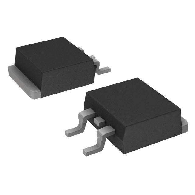
| 描述 | MOSFET N-CH 60V 210A D2PAK |
| 产品分类 | FET - 单 |
| FET功能 | 标准 |
| FET类型 | MOSFET N 通道,金属氧化物 |
| 品牌 | International Rectifier |
| 数据手册 | |
| 产品图片 |
|
| 产品型号 | AUIRFS3206 |
| rohs | 无铅 / 符合限制有害物质指令(RoHS)规范要求 |
| 产品系列 | HEXFET® |
| 不同Id时的Vgs(th)(最大值) | 4V @ 150µA |
| 不同Vds时的输入电容(Ciss) | 6540pF @ 50V |
| 不同Vgs时的栅极电荷(Qg) | 170nC @ 10V |
| 不同 Id、Vgs时的 RdsOn(最大值) | 3 毫欧 @ 75A,10V |
| 产品培训模块 | http://www.digikey.cn/PTM/IndividualPTM.page?site=cn&lang=zhs&ptm=26250 |
| 供应商器件封装 | D2PAK |
| 功率-最大值 | 300W |
| 包装 | 管件 |
| 安装类型 | 表面贴装 |
| 封装/外壳 | TO-263-3,D²Pak(2 引线+接片),TO-263AB |
| 标准包装 | 50 |
| 漏源极电压(Vdss) | 60V |
| 电流-连续漏极(Id)(25°C时) | 120A (Tc) |


- 商务部:美国ITC正式对集成电路等产品启动337调查
- 曝三星4nm工艺存在良率问题 高通将骁龙8 Gen1或转产台积电
- 太阳诱电将投资9.5亿元在常州建新厂生产MLCC 预计2023年完工
- 英特尔发布欧洲新工厂建设计划 深化IDM 2.0 战略
- 台积电先进制程称霸业界 有大客户加持明年业绩稳了
- 达到5530亿美元!SIA预计今年全球半导体销售额将创下新高
- 英特尔拟将自动驾驶子公司Mobileye上市 估值或超500亿美元
- 三星加码芯片和SET,合并消费电子和移动部门,撤换高东真等 CEO
- 三星电子宣布重大人事变动 还合并消费电子和移动部门
- 海关总署:前11个月进口集成电路产品价值2.52万亿元 增长14.8%


PDF Datasheet 数据手册内容提取
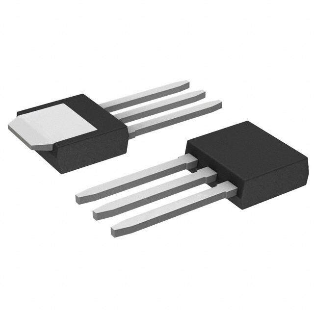
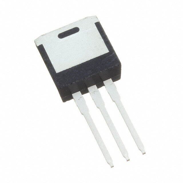
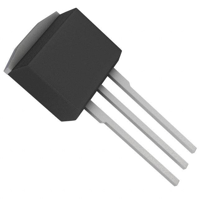
AUIRFS3206 AUTOMOTIVE GRADE AUIRFSL3206 HEXFET® Power MOSFET Features VDSS 60V Advanced Process Technology R typ. 2.4m Ultra Low On-Resistance DS(on) Enhanced dV/dT and dI/dT capability max. 3.0m 175°C Operating Temperature I 210A D (Silicon Limited) Fast Switching I 120A D (Package Limited) Repetitive Avalanche Allowed up to Tjmax Lead-Free, RoHS Compliant Automotive Qualified * D D Description Specifically designed for Automotive applications, this HEXFET® S S Power MOSFET utilizes the latest processing techniques to achieve G G D extremely low on-resistance per silicon area. Additional features of D2Pak TO-262 this design are a 175°C junction operating temperature, fast switching speed and improved repetitive avalanche rating . These AUIRFS3206 AUIRFSL3206 features combine to make this design an extremely efficient and G D S reliable device for use in Automotive applications and a wide variety Gate Drain Source of other applications Standard Pack Base part number Package Type Orderable Part Number Form Quantity AUIRFSL3206 TO-262 Tube 50 AUIRFSL3206 Tube 50 AUIRFS3206 AUIRFS3206 D2-Pak Tape and Reel Left 800 AUIRFS3206TRL Absolute Maximum Ratings Stresses beyond those listed under “Absolute Maximum Ratings” may cause permanent damage to the device. These are stress ratings only; and functional operation of the device at these or any other condition beyond those indicated in the specifications is not implied. Exposure to absolute-maximum-rated conditions for extended periods may affect device reliability. The thermal resistance and power dissipation ratings are measured under board mounted and still air conditions. Ambient temperature (TA) is 25°C, unless otherwise specified. Symbol Parameter Max. Units I @ T = 25°C Continuous Drain Current, V @ 10V (Silicon Limited) 210 D C GS I @ T = 100°C Continuous Drain Current, V @ 10V (Silicon Limited) 150 D C GS A I @ T = 25°C Continuous Drain Current, V @ 10V (Package Limited) 120 D C GS I Pulsed Drain Current 840 DM P @T = 25°C Maximum Power Dissipation 300 W D C Linear Derating Factor 2.0 W/°C V Gate-to-Source Voltage ± 20 V GS E Single Pulse Avalanche Energy (Thermally Limited) 170 mJ AS I Avalanche Current See Fig.14,15, 22a, 22b A AR E Repetitive Avalanche Energy mJ AR dv/dt Peak Diode Recovery 5.0 V/ns T Operating Junction and -55 to + 175 J T Storage Temperature Range °C STG Soldering Temperature, for 10 seconds (1.6mm from case) 300 Thermal Resistance Symbol Parameter Typ. Max. Units R Junction-to-Case ––– 0.50 JC °C/W R Junction-to-Ambient (PCB Mount), D2 Pak ––– 40 JA HEXFET® is a registered trademark of Infineon. *Qualification standards can be found at www.infineon.com 1 2015-10-27
AUIRFS/SL3206 Static @ T = 25°C (unless otherwise specified) J Parameter Min. Typ. Max. Units Conditions V Drain-to-Source Breakdown Voltage 60 ––– ––– V V = 0V, I = 250µA (BR)DSS GS D V /T Breakdown Voltage Temp. Coefficient ––– 0.07 ––– V/°C Reference to 25°C, I = 5mA (BR)DSS J D R Static Drain-to-Source On-Resistance ––– 2.4 3.0 m V = 10V, I = 75A DS(on) GS D V Gate Threshold Voltage 2.0 ––– 4.0 V V = V , I = 150µA GS(th) DS GS D gfs Forward Trans conductance 210 ––– ––– S V = 50V, I = 75A DS D R Gate Resistance ––– 0.7 ––– G ––– ––– 20 V = 60V, V = 0V DS GS I Drain-to-Source Leakage Current µA DSS ––– ––– 250 V = 48V,V = 0V,T =125°C DS GS J I Gate-to-Source Forward Leakage ––– ––– 100 V = 20V GSS nA GS Gate-to-Source Reverse Leakage ––– ––– -100 V = -20V GS Dynamic Electrical Characteristics @ T = 25°C (unless otherwise specified) J Q Total Gate Charge ––– 120 170 I = 75A g D Q Gate-to-Source Charge ––– 29 ––– V = 30V gs DS nC Q Gate-to-Drain Charge ––– 35 ––– V = 10V gd GS Q Total Gate Charge Sync. (Q - Q ) ––– 85 ––– sync g gd t Turn-On Delay Time ––– 19 ––– V = 30V d(on) DD t Rise Time ––– 82 ––– I = 75A r ns D t Turn-Off Delay Time ––– 55 ––– R = 2.7 d(off) G t Fall Time ––– 83 ––– V = 10V f GS C Input Capacitance ––– 6540 ––– V = 0V iss GS C Output Capacitance ––– 720 ––– V = 50V oss DS Crss Reverse Transfer Capacitance ––– 360 ––– pF ƒ = 1.0MHz, See Fig. 5 C Effective Output Capacitance (Energy Related) ––– 1040 ––– V = 0V, V = 0V to 48V oss eff.(ER) GS DS C Effective Output Capacitance (Time Related) ––– 1230 ––– V = 0V, V = 0V to 48V oss eff.(TR) GS DS Diode Characteristics Parameter Min. Typ. Max. Units Conditions Continuous Source Current MOSFET symbol I ––– ––– 210 S (Body Diode) showing the A Pulsed Source Current integral reverse I ––– ––– 840 SM (Body Diode) p-n junction diode. V Diode Forward Voltage ––– ––– 1.3 V T = 25°C,I = 75A,V = 0V SD J S GS ––– 33 50 T = 25°C V = 51V t Reverse Recovery Time ns J DD rr ––– 37 56 T = 125°C I = 75A, J F ––– 41 62 T = 25°C di/dt = 100A/µs Q Reverse Recovery Charge nC J rr ––– 53 80 T = 125°C J I Reverse Recovery Current ––– 2.1 ––– A T = 25°C RRM J t Forward Turn-On Time Intrinsic turn-on time is negligible (turn-on is dominated by L +L ) on S D Notes: Calculated continuous current based on maximum allowable junction temperature. Bond wire current limit is 120A. Note that current limitations arising from heating of the device leads may occur with some lead mounting arrangements. Repetitive rating; pulse width limited by max. junction temperature. Limited by T starting T = 25°C, L = 0.023mH, R = 25, I = 120A, V =10V. Part not recommended for use above this value. Jmax, J G AS GS I 75A, di/dt 360A/µs, V V , T 175°C. SD DD (BR)DSS J Pulse width 400µs; duty cycle 2%. C eff. (TR) is a fixed capacitance that gives the same charging time as C while V is rising from 0 to 80% V . oss oss DS DSS C eff. (ER) is a fixed capacitance that gives the same energy as C while V is rising from 0 to 80% V . oss oss DS DSS When mounted on 1" square PCB (FR-4 or G-10 Material). For recommended footprint and soldering techniques refer to application note #AN-994 R is measured at T approximately 90°C. J 2 2015-10-27
AUIRFS/SL3206 1000 1000 VGS VGS TOP 15V TOP 15V A)ent( 18650...005VVVV A)en(t 18650...005VVVV Cu rre BOTTOM 544...085VVV Cu rre BOTTOM 544...085VVV ucro 100 ucro 100 S S 4.5V o- o- n-t n-t ai ai rD rD , D , D I 4.5V 60µs PULSE WIDTH I 60µs PULSE WIDTH Tj = 25°C Tj = 175°C 10 10 0.1 1 10 100 0.1 1 10 100 VDS, Drain-to-Source Voltage (V) VDS, Drain-to-Source Voltage (V) Fig. 1 Typical Output Characteristics Fig. 2 Typical Output Characteristics 1000 2.5 e c ID = 75A n t )enurr 100 TJ = 175°C atRessiOn 2.0 VGS = 10V Cce ucer d)ze Sourno--itDaI, rD 110 TVJ D6 =0S µ 2=s5 °P2C5UVLSE WIDTH oSo--tanriD, Rn) DoS(aliNmor ( 11..05 0.1 0.5 2.0 3.0 4.0 5.0 6.0 7.0 8.0 -60 -40 -20 0 20 40 60 80 100120140160180 VGS, Gate-to-Source Voltage (V) TJ , Junction Temperature (°C) Fig. 3 Typical Transfer Characteristics Fig. 4 Normalized On-Resistance vs. Temperature 12000 VGS = 0V, f = 1 MHZ 20 I = 75A Ciss = Cgs + Cgd, Cds SHORTED D 10000 Crss = Cgd V) VDS= 48V Coss = Cds + Cgd (ge 16 VDS= 30V Fp) 8000 aolt VDS= 12V ( ce Ciss V e 12 n c atci 6000 uro a S pCa, C 4000 o-tae-t 8 G 2000 Coss , SG 4 V Crss 0 0 1 10 100 0 40 80 120 160 200 VDS, Drain-to-Source Voltage (V) QG Total Gate Charge (nC) Fig 5. Typical Capacitance vs. Drain-to-Source Voltage Fig 6. Typical Gate Charge vs. Gate-to-Source Voltage 3 2015-10-27
AUIRFS/SL3206 1000 10000 OPERATION IN THIS AREA LIMITED BY RDS(on) A()nCu rirentDra 11000 TJ = 175°C TJ = 25°C )An(t eurrCcer ou 1100000 1msec 100µsec verse S-on-t 10 10msec I,Re DS 1 aiD, rID 1 Tc = 25°C Tj = 175°C DC VGS = 0V Single Pulse 0.1 0.1 0.2 0.4 0.6 0.8 1.0 1.2 1.4 1.6 1.8 2.0 0.1 1 10 100 VSD, Source-to-Drain Voltage (V) VDS, Drain-toSource Voltage (V) Fig. 7 Typical Source-to-Drain Diode Fig 8. Maximum Safe Operating Area e 240 g 80 a olt ID = 5mA V 200 Limited By Package wn 75 o d k )Ant( e 160 aeBer 70 urr ucr C 120 o ani So- 65 rD -tn , D 80 Dari I , S 60 40 S D )R B 0 V( 55 25 50 75 100 125 150 175 -60 -40 -20 0 20 40 60 80 100120140160180 TC , Case Temperature (°C) TJ , Junction Temperature (°C) Fig 9. Maximum Drain Current vs. Case Temperature Fig 10. Drain-to-Source Breakdown Voltage 2.0 800 J)m ID y( TOP 21A 1.5 gner 600 B O T T O M 13230AA E e h µJ( )gy 1.0 caanlv 400 ner Ae E s ul P e 0.5 gl 200 n iS S, A E 0.0 0 0 10 20 30 40 50 60 25 50 75 100 125 150 175 VDS, Drain-to-Source Voltage (V) Starting TJ, Junction Temperature (°C) Fig 11. Typical COSS Stored Energy Fig 12. Maximum Avalanche Energy vs. Drain Current 4 2015-10-27
AUIRFS/SL3206 1 D = 0.50 ) C 0.1 0.20 J h 0.10 Zt ( e 0.05 Ri (°C/W) I (sec) sonps 0.01 00..0021 JJ R1R1 R2R2 R3R3 C 0.106416 0.0001 eR lam SINGLE PULSE 1C1iC= i=i RiiRi 22 33 00..210910897283 0.00.001121692212 reh 0.001 ( THERMAL RESPONSE ) T Notes: 1. Duty Factor D = t1/t2 2. Peak Tj = P dm x Zthjc + Tc 0.0001 1E-006 1E-005 0.0001 0.001 0.01 0.1 t1 , Rectangular Pulse Duration (sec) Fig 13. Maximum Effective Transient Thermal Impedance, Junction-to-Case 1000 Duty Cycle = Single Pulse Allowed avalanche Current vs avalanche )A pulsewidth, tav, assuming Tj = 150°C and ( ten 100 0.01 Tstart =25°C (Single Pulse) rru C e h 0.05 c n a 0.10 la 10 v A Allowed avalanche Current vs avalanche pulsewidth, tav, assuming j = 25°C and Tstart = 150°C. 1 1.0E-06 1.0E-05 1.0E-04 1.0E-03 1.0E-02 1.0E-01 tav (sec) Fig 14. Avalanche Current vs. Pulse width 200 Notes on Repetitive Avalanche Curves , Figures 14, 15: TOP Single Pulse (For further info, see AN-1005 at www.infineon.com) BOTTOM 1% Duty Cycle 1. Avalanche failures assumption: )J 160 ID = 120A Purely a thermal phenomenon and failure occurs at a temperature far in m y( excess of Tjmax. This is validated for every part type. ger 2. Safe operation in Avalanche is allowed as long as Tjmax is not exceeded. n 120 3. Equation below based on circuit and waveforms shown in Figures 18a, 18b. E he 4. PD (ave) = Average power dissipation per single avalanche pulse. nc 5. BV = Rated breakdown voltage (1.3 factor accounts for voltage increase a al 80 during avalanche). v A, R 76.. IaTv == AAlllloowwaabbllee arivsael ainn cjuhnec ctiuornr etenmt. perature, not to exceed Tjmax (assumed as A E 40 25°C in Figure 13, 14). tav = Average time in avalanche. D = Duty cycle in avalanche = tav ·f 0 ZthJC(D, tav) = Transient thermal resistance, see Figures 13) 25 50 75 100 125 150 175 Starting TJ , Junction Temperature (°C) PD (ave) = 1/2 ( 1.3·BV·Iav) = T/ ZthJC I = 2T/ [1.3·BV·Z ] av th E = P ·t AS (AR) D (ave) av Fig 15. Maximum Avalanche Energy vs. Temperature 5 2015-10-27
AUIRFS/SL3206 4.5 18 ID = 1.0A 16 V)( e 4.0 ID = 1.0mA 14 ag ID = 250µA lto 3.5 ID = 150µA 12 V dl esho 3.0 A)(- M 10 hr R 8 e t 2.5 IR ta 6 G ) h 2.0 IF = 30A (tS 4 VR = 51V VG 1.5 2 TJ = 125°C TJ = 25°C 1.0 0 -75 -50 -25 0 25 50 75 100 125 150 175 100 200 300 400 500 600 700 800 900 1000 TJ , Temperature ( °C ) dif / dt - (A / µs) Fig 16. Threshold Voltage vs. Temperature Fig. 17 - Typical Recovery Current vs. dif/dt 18 350 16 300 14 250 12 A)(- RM 180 Cn( )- R 200 R R 150 I Q 6 IF = 45A 100 IF = 30A 4 VR = 51V VR = 51V 2 TJ = 125°C 50 TJ = 125°C TJ = 25°C TJ = 25°C 0 0 100 200 300 400 500 600 700 800 900 1000 100 200 300 400 500 600 700 800 900 1000 di / dt - (A / µs) f dif / dt - (A / µs) Fig. 18 - Typical Recovery Current vs. dif/dt Fig. 19 - Typical Stored Charge vs. dif/dt 350 300 250 Cn) 200 ( - R R 150 Q 100 IF = 45A VR = 51V 50 TJ = 125°C TJ = 25°C 0 100 200 300 400 500 600 700 800 900 1000 dif / dt - (A / µs) Fig. 20 - Typical Stored Charge vs. dif/dt 6 2015-10-27
AUIRFS/SL3206 Fig 21. Peak Diode Recovery dv/dt Test Circuit for N-Channel HEXFET® Power MOSFETs 15V V(BR)DSS tp L DRIVER VDS RG D.U.T + - VDD IAS A 20V tp 0.01 IAS Fig 22a. Unclamped Inductive Test Circuit Fig 22b. Unclamped Inductive Waveforms Fig 23a. Switching Time Test Circuit Fig 23b. Switching Time Waveforms Id Vds Vgs Vgs(th) Qgs1 Qgs2 Qgd Qgodr Fig 24a. Gate Charge Test Circuit Fig 24b. Gate Charge Waveform 7 2015-10-27
AUIRFS/SL3206 D2Pak (TO-263AB) Package Outline (Dimensions are shown in millimeters (inches)) D2Pak (TO-263AB) Part Marking Information Part Number AUFS3206 Date Code YWWA IR Logo Y= Year WW= Work Week XX XX Lot Code Note: For the most current drawing please refer to IR website at http://www.irf.com/package/ 8 2015-10-27
AUIRFS/SL3206 TO-262 Package Outline (Dimensions are shown in millimeters (inches) TO-262 Part Marking Information Part Number AUFSL3206 Date Code YWWA IR Logo Y= Year WW= Work Week XX XX Lot Code Note: For the most current drawing please refer to IR website at http://www.irf.com/package/ 9 2015-10-27
AUIRFS/SL3206 D2Pak (TO-263AB) Tape & Reel Information (Dimensions are shown in millimeters (inches)) TRR 1.60 (.063) 1.50 (.059) 1.60 (.063) 4.10 (.161) 3.90 (.153) 1.50 (.059) 0.368 (.0145) 0.342 (.0135) FEED DIRECTION 1.85 (.073) 11.60 (.457) 1.65 (.065) 11.40 (.449) 24.30 (.957) 15.42 (.609) 23.90 (.941) 15.22 (.601) TRL 1.75 (.069) 10.90 (.429) 1.25 (.049) 10.70 (.421) 4.72 (.136) 16.10 (.634) 4.52 (.178) 15.90 (.626) FEED DIRECTION 13.50 (.532) 27.40 (1.079) 12.80 (.504) 23.90 (.941) 4 330.00 60.00 (2.362) (14.173) MIN. MAX. 30.40 (1.197) NOTES : MAX. 1. COMFORMS TO EIA-418. 26.40 (1.039) 4 2. CONTROLLING DIMENSION: MILLIMETER. 24.40 (.961) 3. DIMENSION MEASURED @ HUB. 3 4. INCLUDES FLANGE DISTORTION @ OUTER EDGE. Note: For the most current drawing please refer to IR website at http://www.irf.com/package/ 10 2015-10-27
AUIRFS/SL3206 Qualification Information Automotive (per AEC-Q101) Qualification Level Comments: This part number(s) passed Automotive qualification. Infineon’s Industrial and Consumer qualification level is granted by extension of the higher Automotive level. D2-Pak Moisture Sensitivity Level MSL1 TO-262 Class M4 (+/- 800V)† Machine Model AEC-Q101-002 Class H2 (+/- 4000V)† ESD Human Body Model AEC-Q101-001 Class C5 (+/- 2000V)† Charged Device Model AEC-Q101-005 RoHS Compliant Yes † Highest passing voltage. Revision History Date Comments Updated datasheet with corporate template 10/27/2015 Corrected ordering table on page 1. Published by Infineon Technologies AG 81726 München, Germany © Infineon Technologies AG 2015 All Rights Reserved. IMPORTANT NOTICE The information given in this document shall in no event be regarded as a guarantee of conditions or characteristics (“Beschaffenheitsgarantie”). With respect to any examples, hints or any typical values stated herein and/or any information regarding the application of the product, Infineon Technologies hereby disclaims any and all warranties and liabilities of any kind, including without limitation warranties of non-infringement of intellectual property rights of any third party. In addition, any information given in this document is subject to customer’s compliance with its obligations stated in this document and any applicable legal requirements, norms and standards concerning customer’s products and any use of the product of Infineon Technologies in customer’s applications. The data contained in this document is exclusively intended for technically trained staff. It is the responsibility of customer’s technical departments to evaluate the suitability of the product for the intended application and the completeness of the product information given in this document with respect to such application. For further information on the product, technology, delivery terms and conditions and prices please contact your nearest Infineon Technologies office (www.infineon.com). WARNINGS Due to technical requirements products may contain dangerous substances. For information on the types in question please contact your nearest Infineon Technologies office. Except as otherwise explicitly approved by Infineon Technologies in a written document signed by authorized representatives of Infineon Technologies, Infineon Technologies’ products may not be used in any applications where a failure of the product or any consequences of the use thereof can reasonably be expected to result in personal injury. 11 2015-10-27