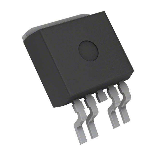
ICGOO在线商城 > 集成电路(IC) > PMIC - 配电开关,负载驱动器 > AUIPS7091G
- 型号: AUIPS7091G
- 制造商: International Rectifier
- 库位|库存: xxxx|xxxx
- 要求:
| 数量阶梯 | 香港交货 | 国内含税 |
| +xxxx | $xxxx | ¥xxxx |
查看当月历史价格
查看今年历史价格
AUIPS7091G产品简介:
ICGOO电子元器件商城为您提供AUIPS7091G由International Rectifier设计生产,在icgoo商城现货销售,并且可以通过原厂、代理商等渠道进行代购。 AUIPS7091G价格参考。International RectifierAUIPS7091G封装/规格:PMIC - 配电开关,负载驱动器, 。您可以下载AUIPS7091G参考资料、Datasheet数据手册功能说明书,资料中有AUIPS7091G 详细功能的应用电路图电压和使用方法及教程。
AUIPS7091G是由英飞凌科技(Infineon Technologies)制造的一款PMIC(电源管理集成电路),属于配电开关和负载驱动器类别。该器件专为汽车应用设计,具有高可靠性和卓越的性能。

应用场景:

1. 车身电子系统:
   - AUIPS7091G广泛应用于车身电子控制系统中,如车窗升降器、座椅调节、后视镜调整等。它能够高效地管理这些系统的电源分配,确保各个部件在不同工作状态下都能获得稳定的电流供应。

2. 信息娱乐系统:
   - 在车载信息娱乐系统中,AUIPS7091G用于管理和保护各种音频、视频设备以及导航系统的电源。它能够快速响应负载变化,确保系统在启动、运行和关闭过程中平稳过渡,避免因电源波动导致的故障。

3. 安全系统:
   - 该器件适用于汽车安全系统,如防抱死制动系统(ABS)、电子稳定程序(ESP)等。AUIPS7091G可以精确控制这些关键系统的电源供给,确保其在紧急情况下仍能正常工作,提高车辆的安全性能。

4. 动力总成系统:
   - 在发动机管理系统和变速器控制单元中,AUIPS7091G负责为传感器、执行器和其他组件提供稳定的电源。它具备出色的抗干扰能力,能够在复杂的电磁环境中保持稳定运行,确保动力系统的可靠性和效率。

5. 辅助驾驶系统:
   - 随着自动驾驶技术的发展,AUIPS7091G也被应用于高级驾驶辅助系统(ADAS)中。它为摄像头、雷达、激光雷达等传感器提供可靠的电源支持,确保数据采集和处理的准确性,从而提升车辆的智能化水平。

总之,AUIPS7091G凭借其高性能、高可靠性以及广泛的适用性,在现代汽车的多个关键系统中发挥着重要作用,满足了汽车行业对电源管理的严格要求。
| 参数 | 数值 |
| 产品目录 | 集成电路 (IC)半导体 |
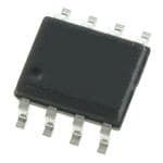
| 描述 | IC HIGH SIDE SWITCH IPS 8SOIC电源开关 IC - 配电 Automotive High side 100mohm IPS 75V |
| 产品分类 | PMIC - MOSFET,电桥驱动器 - 内部开关集成电路 - IC |
| 品牌 | International Rectifier |
| 产品手册 | |
| 产品图片 |
|
| rohs | 符合RoHS无铅 / 符合限制有害物质指令(RoHS)规范要求 |
| 产品系列 | 开关 IC,电源开关 IC - 配电,International Rectifier AUIPS7091G- |
| 数据手册 | |
| 产品型号 | AUIPS7091G |
| 产品培训模块 | http://www.digikey.cn/PTM/IndividualPTM.page?site=cn&lang=zhs&ptm=26250 |
| 产品种类 | 电源开关 IC - 配电 |
| 供应商器件封装 | 8-SOIC |
| 包装 | 管件 |
| 商标 | International Rectifier |
| 安装类型 | 表面贴装 |
| 安装风格 | SMD/SMT |
| 导通电阻 | 80 毫欧 |
| 导通电阻—最大值 | 230 mOhms |
| 封装 | Tube |
| 封装/外壳 | 8-SOIC(0.154",3.90mm 宽) |
| 封装/箱体 | SOIC-8 |
| 工作温度 | -40°C ~ 150°C |
| 工作电源电压 | 6 V to 35 V |
| 工厂包装数量 | 95 |
| 最大功率耗散 | 1.25 W |
| 最大工作温度 | + 150 C |
| 最小工作温度 | - 40 C |
| 标准包装 | 95 |
| 电压-电源 | 6 V ~ 35 V |
| 电流-峰值输出 | 5A |
| 电流-输出/通道 | 1.5A |
| 电流限制 | 5 A |
| 电源电流—最大值 | 4 mA |
| 空闲时间—最大值 | 45 us |
| 类型 | 高端开关 |
| 输入类型 | 非反相 |
| 输出数 | 1 |
| 输出端数量 | 1 Output |
| 运行时间—最大值 | 35 us |




- 商务部:美国ITC正式对集成电路等产品启动337调查
- 曝三星4nm工艺存在良率问题 高通将骁龙8 Gen1或转产台积电
- 太阳诱电将投资9.5亿元在常州建新厂生产MLCC 预计2023年完工
- 英特尔发布欧洲新工厂建设计划 深化IDM 2.0 战略
- 台积电先进制程称霸业界 有大客户加持明年业绩稳了
- 达到5530亿美元!SIA预计今年全球半导体销售额将创下新高
- 英特尔拟将自动驾驶子公司Mobileye上市 估值或超500亿美元
- 三星加码芯片和SET,合并消费电子和移动部门,撤换高东真等 CEO
- 三星电子宣布重大人事变动 还合并消费电子和移动部门
- 海关总署:前11个月进口集成电路产品价值2.52万亿元 增长14.8%



PDF Datasheet 数据手册内容提取
March, 26th 2012 Automotive grade AUIPS7091(G)(S)PbF INTELLIGENT POWER HIGH SIDE SWITCH Features Product Summary Over temperature shutdown (with auto-restart) Short circuit protection (current limit) Rds(on) 120m max. Active clamp Vclamp 70V Open load detection Logic ground isolated from power ground I Limit 5A (typ.) ESD protection Open load 3V Ground loss protection Status feedback Description Package The AUIPS7091(G)(S)PbF is a five terminal Intelligent Power Switch (IPS) with built in short circuit, over- temperature, ESD protection, inductive load capability and diagnostic feedback. The output current is limited at Ilim value. Current limitation is activated until the thermal protection acts. The over-temperature protection turns off the device if the junction temperature exceeds Tshutdown. TO220 D2-Pak SO-8 It will automatically restart after the junction has cooled AUIPS7091PbF AUIPS7091SPbF AUIPS7091GPbF 7°C below Tshutdown. A diagnostic pin is provided for status feedback of short circuit, over-temperature and open load detection. The double level shifter circuitry allows large offsets between the logic ground and the load. Typical Connection +5V +Bat Vcc(5-6-7-8) 15K Dg(3) Control Rdg Pull-up resistor for Open Load Off detection In(2) Gnd(1) Out(4) V Diag Rin Input Signal Load www.irf.com 1
AUIPS7091(G)(S)PbF Qualification Information† Automotive (per AEC-Q100) Qualification Level Comments: This family of ICs has passed an Automotive qualification. IR’s Industrial and Consumer qualification level is granted by extension of the higher Automotive level. MSL1, 260°C D2PAK-5L (per IPC/JEDEC J-STD-020) Moisture Sensitivity Level TO-220 Not applicable (non-surface mount package style) MSL2, 260°C SOIC-8 (per IPC/JEDEC J-STD-020) Class M2 (+/-200V) Machine Model (per AEC-Q100-003) Class H2 (+/-4000V) ESD Human Body Model (per AEC-Q100-002) Class C4 (+/-1000V) Charged Device Model (per AEC-Q100-011) Class II, Level A IC Latch-Up Test (per AEC-Q100-004) RoHS Compliant Yes † Qualification standards can be found at International Rectifier’s web site http://www.irf.com/ www.irf.com 2
AUIPS7091(G)(S)PbF Absolute Maximum Ratings Absolute maximum ratings indicate sustained limits beyond which damage to the device may occur. All voltage parameters are referenced to Ground lead. Tj= -40°C..150°C, Vcc=6..35V (unless otherwise specified). Symbol Parameter Min. Max. Units Vout Maximum output voltage Vcc-63 Vcc+0.3 Voffset Maximum logic ground to load ground offset Vcc-63 Vcc+0.3 Vin Maximum input voltage -0.3 5.5 V Vcc max. Maximum Vcc voltage 60 Vcc cont. Maximum continuous Vcc voltage 35 Vcc sc. Maximum Vcc voltage with short circuit protection with Tj < -10°C 28 Iin max. Maximum IN current -1 10 mA Idg max. Maximum diagnostic output current -1 10 Vdg Maximum diagnostic output voltage -0.3 5.5 V Maximum power dissipation (internally limited by thermal protection) Pd 1.25 W Rth=100°C/W Isd cont. Maximum continuous diode current (Rth=100°C/W) 1.8 A ESD1 Electrostatic discharge voltage (Human body) 100pF, 1500 4 kV ESD2 Electrostatic discharge voltage (Machine Model) C=200pF,R=0,L=10µH 0.5 Tj op max. Max. operating temperature junction temperature -40 +150 °C Tj Sto max. Max. storage temperature junction temperature -55 +150 °C Thermal Characteristics Symbol Parameter Typ. Max. Units Rth1 Thermal resistance junction to ambient SO8 std. footprint 100 Rth1 Thermal resistance junction to ambient TO220 free air 60 Rth1 Thermal resistance junction to ambient D2Pak std. footprint 60 °C/W Rth2 Thermal resistance junction to ambient D2Pak 1” sqrt. footprint 40 Rth3 Thermal resistance junction to case D2pak/TO220 4 Recommended Operating Conditions These values are given for a quick design. For operation outside these conditions, please consult the application notes. Symbol Parameter Min. Max. Units VIH High level input voltage 4 5.5 V VIL Low level input voltage -0.3 0.9 Iout Continuous drain current, Tamb=85°C, Tj=125°C, Vin=5V, Rth=100°C/W 1.5 A Rin Recommended resistor in series with IN pin 10 20 Rdgs Recommended resistor in series with DG pin 10 20 k Rol Recommended pull-up resistor for open load detection 5 100 www.irf.com 3
AUIPS7091(G)(S)PbF Static Electrical Characteristics Tj=-40..150°C, Vcc=6..35V (unless otherwise specified), typical values are given for Vcc=14V and Tj=25°C Symbol Parameter Min. Typ. Max. Units Test Conditions ON state resistance Tj=25°C 80 120 Vin=5V, Iout=2A Rds(on) ON state resistance Tj=150°C 150 230 m Vin=5V, Iout=2A ON state resistance Tj=25°C, Vcc=6.5V 90 130 Vin=5V, Iout=2A Vcc op. Operating voltage range 6 35 V clamp Vcc to Out clamp voltage 63 70 V Iout=30mA (see Fig. 1) Vf Body diode forward voltage 1 1.4 Iout= 2.5A Icc Off Supply current when Off 2.5 10 µA Vin=Vout=0V, Tj=25°C Icc On Supply current when On 2.5 4 mA Vin=5V, Vcc=14V Iout@0V Output leakage current 10 Vout=0V Iout@6V Output leakage current 20 µA Vout=6V Idg leakage Diagnostic output leakage current 10 Vdg=5.5V Vdgl Low level diagnostic output voltage 0.1 0.3 Idg=1.6mA Vih Input high threshold voltage 2.5 3.5 Vil Input low threshold voltage 1 2 In hys Input hysteresis 0.05 0.4 1 V UV high Under voltage high threshold voltage 5 6.2 UV low Under voltage low threshold voltage 3 4.5 5.9 UV hys Under voltage hysteresis 0.1 0.8 1.5 Iin On Input current when device is On 40 80 µA Vin=5V Switching Electrical Characteristics Vcc=14V, Resistive load=6, Vin=5V, Tj=-40°C..150°C, typical values are given for Tj=25°C Symbol Parameter Min. Typ. Max. Units Test Conditions Tdon Turn-on delay time 12 35 Tr1 Rise time to Vout=Vcc-5V 7 40 µs Tr2 Rise time to Vout=0.9 x Vcc 14 50 dV/dt (On) Turn On dV/dt 0.95 5 V/µs EOn Turn On energy 250 µJ See Fig. 3 Tdoff Turn-off delay time 20 45 µs Tf Fall time to Vout=0.1 x Vcc 6 25 dV/dt (Off) Turn Off dV/dt 1.8 5 V/µs EOff Turn Off energy 20 µJ Tdiag Vout to Vdiag propagation delay 15 µs See Fig. 4 and Fig. 12 www.irf.com 4
AUIPS7091(G)(S)PbF Protection Characteristics Tj=-40..150°C, Vcc=6..35V (unless otherwise specified), typical values are given for Vcc=14V and Tj=25°C Symbol Parameter Min. Typ. Max. Units Test Conditions Ilim Internal current limit 2 5 8 A Vout=0V, Tj=25°C Tsd+ Over temperature high threshold 150(1) 165 °C See Fig. 2 Tsd- Over temperature low threshold 158 Vsc Short-circuit detection voltage (2) 2 3 4 V Vopen load Open load detection threshold 2 3 4 (1) Guaranteed by design (2) Reference to Vcc Truth Table Operating Conditions IN OUT DG pin Normal H H H Normal L L L Open Load H H H Open Load (3) L H H Short circuit to Gnd H L (limiting) L Short circuit to Gnd L L L Over-temperature H L (cycling) L Over-temperature L L L (3) With a pull-up resistor connected between the output and Vcc. Lead Assignments www.irf.com 5
AUIPS7091(G)(S)PbF Functional Block Diagram All values are typical VCC 165°C Tj 66V 75V 158°C Charge Pump Vcc-Gnd >UV 2.5V Level Driver 75V IN Shifter 2.0V 6V k 0 5 1 Gnd Loss Protection - + I Sense I Limit DG Open Load - + 6V - 3V Short Circuit + 3V 0 3 GND OUT www.irf.com 6
AUIPS7091(G)(S)PbF Vin T clamp Vin Iout limiting Thermal cycling Ids Ilim Vds clamp Tj Tsd+ Vds Tsd- Vcc See Application Notes to evaluate power dissipation Figure 1 – Active clamp waveforms Figure 2 – Protection timing diagram 90% Vin Vin Vih Vil 10% Vout Vcc Vcc - Vsc 90% Vcc-5V Vout 10% Td on Td off Vol Tr1 Tf Vdg Tr2 Vds Blanking Blanking Diag ON Tdiag Diag OFF Figure 3 – Switching times definition Figure 4 – Diagnostic delay definition www.irf.com 7
AUIPS7091(G)(S)PbF 10 A) Dg Vcc Vclamp ent ( In Gnd Out urr 1 L 14V+ put c - ut 5V O 0V Vin RemV : out R out, During active I clamp, Iout Vload is 0.1 negative 1E+2 1E+3 1E+4 1E+5 1E+6 Load inductance (µH) Figure 5 – Active clamp test circuit Figure 6 – Max. Output current (A) Vs Load inductance (µH) 5 100.0 W) C/ A) 4 e (° urrent ( 3 pedanc 10.0 c m put al i ut 2 m O er 1.0 s, cont. 1 sient th d n I a 0 h, tr 0.1 -50 0 50 100 150 Zt 0.0001 0.001 0.01 0.1 1 10 100 Tamb, Ambient temperature (°C) Time (s) Figure 7 – Max. ouput current (A) Figure 8 – Transient thermal impedance (°C/W) Vs Ambient temperature (°C) Rth=100°C/W Vs time (s) www.irf.com 8
AUIPS7091(G)(S)PbF 7 500 6 J) µ 5 y ( g 400 er A) 4 g en mit ( 3 chin Eon I li 2 off, swit 300 Eoff E 1 n, Eo 200 0 -50 0 50 100 150 Tj, junction temperature (°C) Iout, Output current (A) 100 Figure 9 –I limit (A) Figure 10 – Switching energy (µJ) Vs junction temperature (°C) Vs Output current (A) 0 200% 0 1 2 3 4 60 e c n a st si e n R 150% s) 50 Source Omalized) g time ( n-to-(Nor 100% ankin 40 Tdiag on ai Bl Dr n), Tdiag off o s( 50% Rd -50 0 50 100 150 30 Tj, junction temperature (°C) Output current (A) Figure 12 – Diagnostic Blanking time (s) 20 Figure 11 - Normalized Rds(on) (%) Vs Tj (°C) Vs Output current (A) www.irf.com 9 10 0 0 1 2 3
AUIPS7091(G)(S)PbF 1.E+4 1.E+4 A) A) µ µ nt ( 1.E+3 nt ( 1.E+3 e Icc on e Icc on curr Icc off curr Icc off ply 1.E+2 ply 1.E+2 p p u u s s c off, 1.E+1 c off, 1.E+1 c c n/ I n/ I o o c c Ic 1.E+0 Ic 1.E+0 0 5 10 15 20 25 30 35 -50 0 50 100 150 Vcc, power supply voltage (V) Tj, junction temperature (°C) Figure 13 – Icc on/ Icc off (µA) Vs Vcc (V) Figure 14 – Icc on/ Icc off (µA) Vs Tj (°C) www.irf.com 10
AUIPS7091(G)(S)PbF Case outline - TO220 www.irf.com 11
AUIPS7091(G)(S)PbF Case outline – D²Pak www.irf.com 12
AUIPS7091(G)(S)PbF Tape and reel – D²Pak www.irf.com 13
AUIPS7091(G)(S)PbF Case Outline - SO-8 www.irf.com 14
AUIPS7091(G)(S)PbF Tape & Reel - SO-8 www.irf.com 15
AUIPS7091(G)(S)PbF Part Marking Information www.irf.com 16
AUIPS7091(G)(S)PbF Ordering Information Standard Pack Base Part Number Package Type Complete Part Number Form Quantity AUIPS7091 TO220-5-Leads Tube 50 AUIPS7091 Tube 50 AUIPS7091S AUIPS7091S D2-Pak-5-Leads Tape and reel left 800 AUIPS7091STRL Tape and reel right 800 AUIPS7091STRR Tube 95 AUIPS7091G AUIPS7091G SOIC-8 Tape and reel 2500 AUIPS7091GTR www.irf.com 17
AUIPS7091(G)(S)PbF IMPORTANT NOTICE Unless specifically designated for the automotive market, International Rectifier Corporation and its subsidiaries (IR) reserve the right to make corrections, modifications, enhancements, improvements, and other changes to its products and services at any time and to discontinue any product or services without notice. Part numbers designated with the “AU” prefix follow automotive industry and / or customer specific requirements with regards to product discontinuance and process change notification. All products are sold subject to IR’s terms and conditions of sale supplied at the time of order acknowledgment. IR warrants performance of its hardware products to the specifications applicable at the time of sale in accordance with IR’s standard warranty. Testing and other quality control techniques are used to the extent IR deems necessary to support this warranty. Except where mandated by government requirements, testing of all parameters of each product is not necessarily performed. IR assumes no liability for applications assistance or customer product design. Customers are responsible for their products and applications using IR components. To minimize the risks with customer products and applications, customers should provide adequate design and operating safeguards. Reproduction of IR information in IR data books or data sheets is permissible only if reproduction is without alteration and is accompanied by all associated warranties, conditions, limitations, and notices. Reproduction of this information with alterations is an unfair and deceptive business practice. IR is not responsible or liable for such altered documentation. Information of third parties may be subject to additional restrictions. Resale of IR products or serviced with statements different from or beyond the parameters stated by IR for that product or service voids all express and any implied warranties for the associated IR product or service and is an unfair and deceptive business practice. IR is not responsible or liable for any such statements. IR products are not designed, intended, or authorized for use as components in systems intended for surgical implant into the body, or in other applications intended to support or sustain life, or in any other application in which the failure of the IR product could create a situation where personal injury or death may occur. Should Buyer purchase or use IR products for any such unintended or unauthorized application, Buyer shall indemnify and hold International Rectifier and its officers, employees, subsidiaries, affiliates, and distributors harmless against all claims, costs, damages, and expenses, and reasonable attorney fees arising out of, directly or indirectly, any claim of personal injury or death associated with such unintended or unauthorized use, even if such claim alleges that IR was negligent regarding the design or manufacture of the product. Only products certified as military grade by the Defense Logistics Agency (DLA) of the US Department of Defense, are designed and manufactured to meet DLA military specifications required by certain military, aerospace or other applications. Buyers acknowledge and agree that any use of IR products not certified by DLA as military-grade, in applications requiring military grade products, is solely at the Buyer’s own risk and that they are solely responsible for compliance with all legal and regulatory requirements in connection with such use. IR products are neither designed nor intended for use in automotive applications or environments unless the specific IR products are designated by IR as compliant with ISO/TS 16949 requirements and bear a part number including the designation “AU”. Buyers acknowledge and agree that, if they use any non-designated products in automotive applications, IR will not be responsible for any failure to meet such requirements. For technical support, please contact IR’s Technical Assistance Center http://www.irf.com/technical-info/ WORLD HEADQUARTERS: 101 N. Sepulveda Blvd., El Segundo, California 90245 Tel: (310) 252-7105 www.irf.com 18
AUIPS7091(G)(S)PbF Revision History Revision Date Notes/Changes A1 October 2011 First release B March 2012 Remove the preliminary mention www.irf.com 19
Mouser Electronics Authorized Distributor Click to View Pricing, Inventory, Delivery & Lifecycle Information: I nfineon: AUIPS7091G
 Datasheet下载

