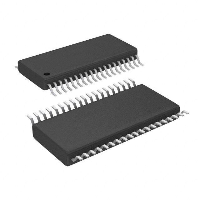
ICGOO在线商城 > 集成电路(IC) > 嵌入式 - 微控制器 > ATTINY28L-4MU
- 型号: ATTINY28L-4MU
- 制造商: Atmel
- 库位|库存: xxxx|xxxx
- 要求:
| 数量阶梯 | 香港交货 | 国内含税 |
| +xxxx | $xxxx | ¥xxxx |
查看当月历史价格
查看今年历史价格
ATTINY28L-4MU产品简介:
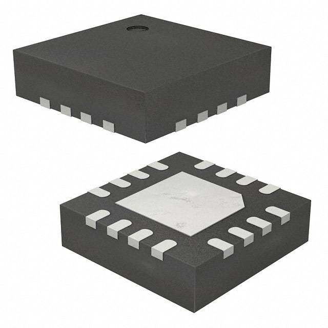
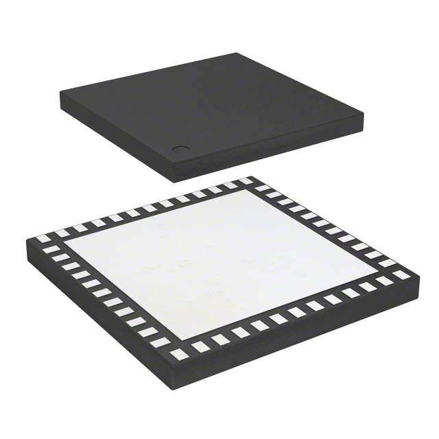
ICGOO电子元器件商城为您提供ATTINY28L-4MU由Atmel设计生产,在icgoo商城现货销售,并且可以通过原厂、代理商等渠道进行代购。 ATTINY28L-4MU价格参考。AtmelATTINY28L-4MU封装/规格:嵌入式 - 微控制器, AVR 微控制器 IC AVR® ATtiny 8-位 4MHz 2KB(1K x 16) 闪存 32-VQFN(5x5)。您可以下载ATTINY28L-4MU参考资料、Datasheet数据手册功能说明书,资料中有ATTINY28L-4MU 详细功能的应用电路图电压和使用方法及教程。
Microchip Technology的ATTINY28L-4MU是一款小型、低功耗的8位AVR微控制器,适用于多种嵌入式控制系统。其主要应用场景包括:

1. 消费电子产品:如遥控器、玩具、小家电等,因其低功耗和小封装,适合电池供电设备。

2. 工业控制:用于传感器节点、电机控制、开关控制等简单自动化任务,适合在恶劣环境中稳定运行。

3. 智能卡与安全设备:ATTINY28L-4MU具备一定的安全特性,可用于门禁系统、电子锁等安全相关设备。

4. 教育与DIY项目:由于其成本低、开发资源丰富,常用于教学实验和电子爱好者项目中,如LED控制、简易机器人等。

5. 物联网(IoT)节点:作为边缘设备中的主控单元,处理传感器数据采集与简单通信任务,尤其适合与无线模块结合使用。

6. 汽车电子:用于车内灯光控制、车窗控制等低复杂度应用,满足汽车环境下的可靠性要求。

该芯片采用TQFP封装,具备2KB Flash存储器和128B SRAM,适合资源受限但要求高效能比的场景。
| 参数 | 数值 |
| 产品目录 | 集成电路 (IC) |
| 描述 | IC MCU 8BIT 2KB FLASH 32QFN |
| EEPROM容量 | - |
| 产品分类 | |
| I/O数 | 11 |
| 品牌 | Atmel |
| 数据手册 | |
| 产品图片 |
|
| 产品型号 | ATTINY28L-4MU |
| PCN其它 | |
| PCN设计/规格 | |
| RAM容量 | - |
| rohs | 无铅 / 符合限制有害物质指令(RoHS)规范要求 |
| 产品系列 | AVR® ATtiny |
| 产品培训模块 | http://www.digikey.cn/PTM/IndividualPTM.page?site=cn&lang=zhs&ptm=24997http://www.digikey.cn/PTM/IndividualPTM.page?site=cn&lang=zhs&ptm=25784http://www.digikey.cn/PTM/IndividualPTM.page?site=cn&lang=zhs&ptm=26162http://www.digikey.cn/PTM/IndividualPTM.page?site=cn&lang=zhs&ptm=26159http://www.digikey.cn/PTM/IndividualPTM.page?site=cn&lang=zhs&ptm=26180 |
| 产品目录页面 | |
| 供应商器件封装 | 32-QFN(5x5) |
| 其它名称 | ATTINY28L4MU |
| 包装 | 托盘 |
| 外设 | POR,WDT |
| 封装/外壳 | 32-VFQFN 裸露焊盘 |
| 工作温度 | -40°C ~ 85°C |
| 振荡器类型 | 内部 |
| 数据转换器 | - |
| 标准包装 | 490 |
| 核心处理器 | AVR |
| 核心尺寸 | 8-位 |
| 电压-电源(Vcc/Vdd) | 2.7 V ~ 5.5 V |
| 程序存储器类型 | 闪存 |
| 程序存储容量 | 2KB(1K x 16) |
| 连接性 | - |
| 速度 | 4MHz |
| 配用 | /product-detail/zh/ATSTK600-DIP40/ATSTK600-DIP40-ND/1812222/product-detail/zh/ATSTK500/ATSTK500-ND/355495 |







- 商务部:美国ITC正式对集成电路等产品启动337调查
- 曝三星4nm工艺存在良率问题 高通将骁龙8 Gen1或转产台积电
- 太阳诱电将投资9.5亿元在常州建新厂生产MLCC 预计2023年完工
- 英特尔发布欧洲新工厂建设计划 深化IDM 2.0 战略
- 台积电先进制程称霸业界 有大客户加持明年业绩稳了
- 达到5530亿美元!SIA预计今年全球半导体销售额将创下新高
- 英特尔拟将自动驾驶子公司Mobileye上市 估值或超500亿美元
- 三星加码芯片和SET,合并消费电子和移动部门,撤换高东真等 CEO
- 三星电子宣布重大人事变动 还合并消费电子和移动部门
- 海关总署:前11个月进口集成电路产品价值2.52万亿元 增长14.8%



PDF Datasheet 数据手册内容提取
Features • Utilizes the AVR® RISC Architecture (cid:129) AVR – High-performance and Low-power RISC Architecture – 90 Powerful Instructions – Most Single Clock Cycle Execution – 32 x 8 General-purpose Working Registers – Up to 4 MIPS Throughput at 4 MHz (cid:129) Nonvolatile Program Memory – 2K Bytes of Flash Program Memory – Endurance: 1,000 Write/Erase Cycles – Programming Lock for Flash Program Data Security (cid:129) Peripheral Features 8-bit – Interrupt and Wake-up on Low-level Input – One 8-bit Timer/Counter with Separate Prescaler Microcontroller – On-chip Analog Comparator – Programmable Watchdog Timer with On-chip Oscillator with 2K Bytes of – Built-in High-current LED Driver with Programmable Modulation (cid:129) Special Microcontroller Features Flash – Low-power Idle and Power-down Modes – External and Internal Interrupt Sources – Power-on Reset Circuit with Programmable Start-up Time – Internal Calibrated RC Oscillator ATtiny28L (cid:129) Power Consumption at 1 MHz, 2V, 25°C – Active: 3.0 mA ATtiny28V – Idle Mode: 1.2 mA – Power-down Mode: <1 µA (cid:129) I/O and Packages – 11 Programmable I/O Lines, 8 Input Lines and a High-current LED Driver – 28-lead PDIP, 32-lead TQFP, and 32-pad MLF Summary (cid:129) Operating Voltages – V : 1.8V - 5.5V for the ATtiny28V CC – V : 2.7V - 5.5V for the ATtiny28L CC (cid:129) Speed Grades – 0 - 1.2 MHz for the ATtiny28V – 0 - 4 MHz For the ATtiny28L Pin Configurations PDIP TQFP/QFN/MLF T R) RESET 1 28 PA0 D2D1D0ESEA0A1A3A2 (I PPPRPPPP PD0 2 27 PA1 PD1 3 26 PA3 3231302928272625 PD2 4 25 PA2 (IR) PD3 1 24 PB7 PD3 5 24 PB7 PD4 2 23 PB6 PD4 6 23 PB6 NC 3 22 NC VCC 7 22 GND VCC 4 21 GND GND 8 21 NC GND 5 20 NC XTAL1 9 20 VCC NC 6 19 NC XTAL1 7 18 VCC XTAL2 10 19 PB5 XTAL2 8 17 PB5 PD5 11 18 PB4 (INT1) PD6 12 17 PB3 (INT0) 910111213141516 PD7 13 16 PB2 (T0) 56701234 (AIN0) PB0 14 15 PB1 (AIN1) PDPDPDPBPBPBPBPB 0) 1) 0) 0) 1) NNTTT (AI(AI((IN(IN Rev. 1062FS–AVR–07/06 Note: This is a summary document. A complete document 1 is available on our Web site at www.atmel.com.
Description The ATtiny28 is a low-power CMOS 8-bit microcontroller based on the AVR RISC archi- tecture. By executing powerful instructions in a single clock cycle, the ATtiny28 achieves throughputs approaching 1 MIPS per MHz, allowing the system designer to optimize power consumption versus processing speed. The AVR core combines a rich instruction set with 32 general-purpose working registers. All the 32 registers are directly con- nected to the Arithmetic Logic Unit (ALU), allowing two independent registers to be accessed in one single instruction executed in one clock cycle. The resulting architec- ture is more code efficient while achieving throughputs up to ten times faster than conventional CISC microcontrollers. Block Diagram Figure 1. The ATtiny28 Block Diagram VCC XTAL1 XTAL2 8-BIT DATA BUS INTERNAL OISNCTIELRLANTAOLR OSCILLATOR OCASLCIIBLRLAATTOEDR GND PROGRAM STACK WATCHDOG TIMING AND RESET COUNTER POINTER TIMER CONTROL PROGRAM HARDWARE MCU CONTROL FLASH STACK REGISTER INSTRUCTION TIMER/ REGISTER GENERAL COUNTER PURPOSE REGISTERS INSTRUCTION INTERRUPT DECODER Z UNIT CONTROL ALU LINES STATUS REGISTER HARDWARE MODULATOR PROGRAMMING LOGIC R O +- ALOGARATDATAP ROERGTBISTER DATAP ROERGTDISTER REDGAT. PAO DRIRTD DATAP ROERGTAISTER PORRTEAG CISOTNETRROL NP AM O C PORTB PORTD PORTA The ATtiny28 provides the following features: 2K bytes of Flash, 11 general-purpose I/O lines, 8 input lines, a high-current LED driver, 32 general-purpose working registers, an 8-bit timer/counter, internal and external interrupts, programmable Watchdog Timer with internal oscillator and 2 software-selectable power-saving modes. The Idle Mode stops the CPU while allowing the timer/counter and interrupt system to continue functioning. The Power-down mode saves the register contents but freezes the oscillator, disabling all other chip functions until the next interrupt or hardware reset. The wake-up or inter- ATtiny28L/V 2 1062FS–AVR–07/06
ATtiny28L/V rupt on low-level input feature enables the ATtiny28 to be highly responsive to external events, still featuring the lowest power consumption while in the power-down modes. The device is manufactured using Atmel’s high-density, nonvolatile memory technology. By combining an enhanced RISC 8-bit CPU with Flash on a monolithic chip, the Atmel ATtiny28 is a powerful microcontroller that provides a highly flexible and cost-effective solution to many embedded control applications. The ATtiny28 AVR is supported with a full suite of program and system development tools including: macro assemblers, pro- gram debugger/simulators, in-circuit emulators and evaluation kits. Pin Descriptions VCC Supply voltage pin. GND Ground pin. Port A (PA3..PA0) Port A is a 4-bit I/O port. PA2 is output-only and can be used as a high-current LED driver. At V = 2.0V, the PA2 output buffer can sink 25 mA. PA3, PA1 and PA0 are CC bi-directional I/O pins with internal pull-ups (selected for each bit). The port pins are tri- stated when a reset condition becomes active, even if the clock is not running. Port B (PB7..PB0) Port B is an 8-bit input port with internal pull-ups (selected for all Port B pins). Port B pins that are externally pulled low will source current if the pull-ups are activated. Port B also serves the functions of various special features of the ATtiny28 as listed on page 27. If any of the special features are enabled, the pull-up(s) on the corresponding pin(s) is automatically disabled. The port pins are tri-stated when a reset condition becomes active, even if the clock is not running. Port D (PD7..PD0) Port D is an 8-bit I/O port. Port pins can provide internal pull-up resistors (selected for each bit). The port pins are tri-stated when a reset condition becomes active, even if the clock is not running. XTAL1 Input to the inverting oscillator amplifier and input to the internal clock operating circuit. XTAL2 Output from the inverting oscillator amplifier. RESET Reset input. An external reset is generated by a low level on the RESET pin. Reset pulses longer than 50 ns will generate a reset, even if the clock is not running. Shorter pulses are not guaranteed to generate a reset. 3 1062FS–AVR–07/06
Register Summary Address Name Bit 7 Bit 6 Bit 5 Bit 4 Bit 3 Bit 2 Bit 1 Bit 0 Page $3F SREG I T H S V N Z C page 6 $3E Reserved ... Reserved $20 Reserved $1F Reserved $1E Reserved $1D Reserved $1C Reserved $1B PORTA - - - - PORTA3 PORTA2 PORTA1 PORTA0 page 32 $1A PACR - - - - DDA3 PA2HC DDA1 DDA0 page 32 $19 PINA - - - - PINA3 - PINA1 PINA0 page 32 $18 Reserved $17 Reserved $16 PINB PINB7 PINB6 PINB5 PINB4 PINB3 PINB2 PINB1 PINB0 page 32 $15 Reserved $14 Reserved $13 Reserved $12 PORTD PORTD7 PORTD6 PORTD5 PORTD4 PORTD3 PORTD2 PORTD1 PORTD0 page 33 $11 DDRD DDD7 DDD6 DDD5 DDD4 DDD3 DDD2 DDD1 DDD0 page 33 $10 PIND PIND7 PIND6 PIND5 PIND4 PIND3 PIND2 PIND1 PIND0 page 33 $0F Reserved $0E Reserved $0D Reserved $0C Reserved $0B Reserved $0A Reserved $09 Reserved $08 ACSR ACD - ACO ACI ACIE - ACIS1 ACIS0 page 44 $07 MCUCS PLUPB - SE SM WDRF - EXTRF PORF page 19 $06 ICR INT1 INT0 LLIE TOIE0 ISC11 ISC10 ISC01 ISC00 page 22 $05 IFR INTF1 INTF0 - TOV0 - - - - page 23 $04 TCCR0 FOV0 - - OOM01 OOM00 CS02 CS01 CS00 page 35 $03 TCNT0 Timer/Counter0 (8-bit) page 36 $02 MODCR ONTIM4 ONTIM3 ONTIM2 ONTIM1 ONTIM0 MCONF2 MCONF1 MCONF0 page 43 $01 WDTCR - - - WDTOE WDE WDP2 WDP1 WDP0 page 37 $00 OSCCAL Oscillator Calibration Register page 9 Notes: 1. For compatibility with future devices, reserved bits should be written to zero if accessed. Reserved I/O memory addresses should never be written. 2. Some of the status flags are cleared by writing a logical “1” to them. Note that the CBI and SBI instructions will operate on all bits in the I/O register, writing a one back into any flag read as set, thus clearing the flag. The CBI and SBI instructions work with registers $00 to $1F only. ATtiny28L/V 4 1062FS–AVR–07/06
ATtiny28L/V Instruction Set Summar y Mnemonic Operands Description Operation Flags # Clocks ARITHMETIC AND LOGIC INSTRUCTIONS ADD Rd, Rr Add Two Registers Rd ← Rd + Rr Z,C,N,V,H 1 ADC Rd, Rr Add with Carry Two Registers Rd ← Rd + Rr + C Z,C,N,V,H 1 SUB Rd, Rr Subtract Two Registers Rd ← Rd - Rr Z,C,N,V,H 1 SUBI Rd, K Subtract Constant from Register Rd ← Rd - K Z,C,N,V,H 1 SBC Rd, Rr Subtract with Carry Two Registers Rd ← Rd - Rr - C Z,C,N,V,H 1 SBCI Rd, K Subtract with Carry Constant from Reg. Rd ← Rd - K - C Z,C,N,V,H 1 AND Rd, Rr Logical AND Registers Rd ← Rd • Rr Z,N,V 1 ANDI Rd, K Logical AND Register and Constant Rd ← Rd • K Z,N,V 1 OR Rd, Rr Logical OR Registers Rd ← Rd v Rr Z,N,V 1 ORI Rd, K Logical OR Register and Constant Rd ← Rd v K Z,N,V 1 EOR Rd, Rr Exclusive OR Registers Rd ← Rd ⊕ Rr Z,N,V 1 COM Rd One’s Complement Rd ← $FF - Rd Z,C,N,V 1 NEG Rd Two’s Complement Rd ← $00 - Rd Z,C,N,V,H 1 SBR Rd, K Set Bit(s) in Register Rd ← Rd v K Z,N,V 1 CBR Rd, K Clear Bit(s) in Register Rd ← Rd • (FFh - K) Z,N,V 1 INC Rd Increment Rd ← Rd + 1 Z,N,V 1 DEC Rd Decrement Rd ← Rd - 1 Z,N,V 1 TST Rd Test for Zero or Minus Rd ← Rd • Rd Z,N,V 1 CLR Rd Clear Register Rd ← Rd ⊕ Rd Z,N,V 1 SER Rd Set Register Rd ← $FF None 1 BRANCH INSTRUCTIONS RJMP k Relative Jump PC ← PC + k + 1 None 2 RCALL k Relative Subroutine Call PC ← PC + k + 1 None 3 RET Subroutine Return PC ← STACK None 4 RETI Interrupt Return PC ← STACK I 4 CPSE Rd, Rr Compare, Skip if Equal if (Rd = Rr) PC ← PC + 2 or 3 None 1/2 CP Rd, Rr Compare Rd - Rr Z,N,V,C,H 1 CPC Rd, Rr Compare with Carry Rd - Rr - C Z,N,V,C,H 1 CPI Rd, K Compare Register with Immediate Rd - K Z N,V,C,H 1 SBRC Rr, b Skip if Bit in Register Cleared if (Rr(b) = 0) PC ← PC + 2 or 3 None 1/2 SBRS Rr, b Skip if Bit in Register is Set if (Rr(b) = 1) PC ← PC + 2 or 3 None 1/2 SBIC P, b Skip if Bit in I/O Register Cleared if (P(b) = 0) PC ← PC + 2 or 3 None 1/2 SBIS P, b Skip if Bit in I/O Register is Set if (P(b) = 1) PC ← PC + 2 or 3 None 1/2 BRBS s, k Branch if Status Flag Set if (SREG(s) = 1) then PC ← PC + k + 1 None 1/2 BRBC s, k Branch if Status Flag Cleared if (SREG(s) = 0) then PC ← PC + k + 1 None 1/2 BREQ k Branch if Equal if (Z = 1) then PC ← PC + k + 1 None 1/2 BRNE k Branch if Not Equal if (Z = 0) then PC ← PC + k + 1 None 1/2 BRCS k Branch if Carry Set if (C = 1) then PC ← PC + k + 1 None 1/2 BRCC k Branch if Carry Cleared if (C = 0) then PC ← PC + k + 1 None 1/2 BRSH k Branch if Same or Higher if (C = 0) then PC ← PC + k + 1 None 1/2 BRLO k Branch if Lower if (C = 1) then PC ← PC + k + 1 None 1/2 BRMI k Branch if Minus if (N = 1) then PC ← PC + k + 1 None 1/2 BRPL k Branch if Plus if (N = 0) then PC ← PC + k + 1 None 1/2 BRGE k Branch if Greater or Equal, Signed if (N ⊕ V = 0) then PC ← PC + k + 1 None 1/2 BRLT k Branch if Less than Zero, Signed if (N ⊕ V = 1) then PC ← PC + k + 1 None 1/2 BRHS k Branch if Half-carry Flag Set if (H = 1) then PC ← PC + k + 1 None 1/2 BRHC k Branch if Half-carry Flag Cleared if (H = 0) then PC ← PC + k + 1 None 1/2 BRTS k Branch if T-flag Set if (T = 1) then PC ← PC + k + 1 None 1/2 BRTC k Branch if T-flag Cleared if (T = 0) then PC ← PC + k + 1 None 1/2 BRVS k Branch if Overflow Flag is Set if (V = 1) then PC ← PC + k + 1 None 1/2 BRVC k Branch if Overflow Flag is Cleared if (V = 0) then PC ← PC + k + 1 None 1/2 BRIE k Branch if Interrupt Enabled if (I = 1) then PC ← PC + k + 1 None 1/2 BRID k Branch if Interrupt Disabled if (I = 0) then PC ← PC + k + 1 None 1/2 5 1062FS–AVR–07/06
Instruction Set Summary (Continued) Mnemonic Operands Description Operation Flags # Clocks DATA TRANSFER INSTRUCTIONS LD Rd, Z Load Register Indirect Rd ← (Z) None 2 ST Z, Rr Store Register Indirect (Z) ← Rr None 2 MOV Rd, Rr Move between Registers Rd ← Rr None 1 LDI Rd, K Load Immediate Rd ← K None 1 IN Rd, P In Port Rd ← P None 1 OUT P, Rr Out Port P ← Rr None 1 LPM Load Program Memory R0 ← (Z) None 3 BIT AND BIT-TEST INSTRUCTIONS SBI P, b Set Bit in I/O Register I/O(P,b) ← 1 None 2 CBI P, b Clear Bit in I/O Register I/O(P,b) ← 0 None 2 LSL Rd Logical Shift Left Rd(n+1) ← Rd(n), Rd(0) ← 0 Z,C,N,V 1 LSR Rd Logical Shift Right Rd(n) ← Rd(n+1), Rd(7) ← 0 Z,C,N,V 1 ROL Rd Rotate Left through Carry Rd(0) ← C, Rd(n+1) ← Rd(n), C ← Rd(7) Z,C,N,V 1 ROR Rd Rotate Right through Carry Rd(7) ← C, Rd(n) ← Rd(n+1), C ← Rd(0) Z,C,N,V 1 ASR Rd Arithmetic Shift Right Rd(n) ← Rd(n+1), n = 0..6 Z,C,N,V 1 SWAP Rd Swap Nibbles Rd(3..0) ← Rd(7..4), Rd(7..4) ← Rd(3..0) None 1 BSET s Flag Set SREG(s) ← 1 SREG(s) 1 BCLR s Flag Clear SREG(s) ← 0 SREG(s) 1 BST Rr, b Bit Store from Register to T T ← Rr(b) T 1 BLD Rd, b Bit Load from T to Register Rd(b) ← T None 1 SEC Set Carry C ← 1 C 1 CLC Clear Carry C ← 0 C 1 SEN Set Negative Flag N ← 1 N 1 CLN Clear Negative Flag N ← 0 N 1 SEZ Set Zero Flag Z ← 1 Z 1 CLZ Clear Zero Flag Z ← 0 Z 1 SEI Global Interrupt Enable I ← 1 I 1 CLI Global Interrupt Disable I ← 0 I 1 SES Set Signed Test Flag S ← 1 S 1 CLS Clear Signed Test Flag S ← 0 S 1 SEV Set Two’s Complement Overflow V ← 1 V 1 CLV Clear Two’s Complement Overflow V ← 0 V 1 SET Set T in SREG T ← 1 T 1 CLT Clear T in SREG T ← 0 T 1 SEH Set Half-carry Flag in SREG H ← 1 H 1 CLH Clear Half-carry Flag in SREG H ← 0 H 1 NOP No Operation None 1 SLEEP Sleep (see specific descr. for Sleep function) None 1 WDR Watchdog Reset (see specific descr. for WDR/timer) None 1 ATtiny28L/V 6 1062FS–AVR–07/06
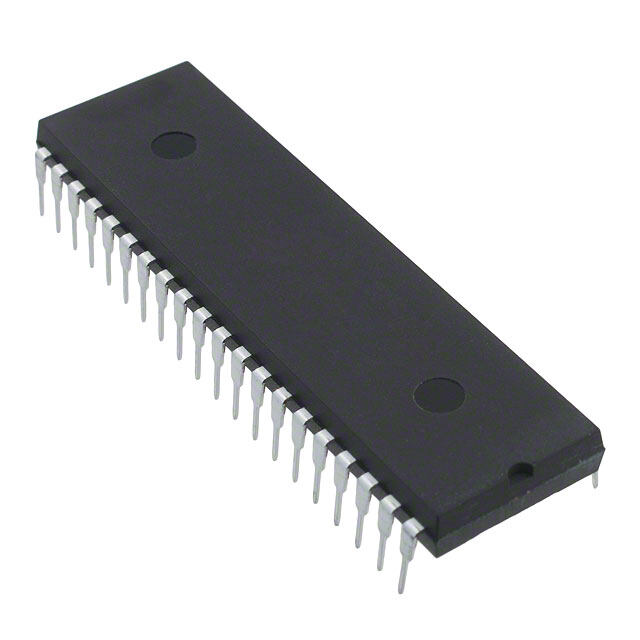
ATtiny28L/V Ordering Information Speed (MHz) Power Supply (Volts) Ordering Code Package(1) Operation Range ATtiny28L-4AC 32A Commercial ATtiny28L-4PC 28P3 (0°C to 70°C) ATtiny28L-4MC 32M1-A ATtiny28L-4AI 32A 4 2.7 - 5.5 ATtiny28L-4AU(2) 32A ATtiny28L-4PI 28P3 Industrial ATtiny28L-4PU(2) 28P3 (-40°C to 85°C) ATtiny28L-4MI 32M1-A ATtiny28L-4MU(2) 32M1-A ATtiny28V-1AC 32A Commercial ATtiny28V-1PC 28P3 (0°C to 70°C) ATtiny28V-1MC 32M1-A ATtiny28V-1AI 32A 1.2 1.8 - 5.5 ATtiny28V-1AU(2) 32A ATtiny28V-1PI 28P3 Industrial ATtiny28V-1PU(2) 28P3 (-40°C to 85°C) ATtiny28V-1MI 32M1-A ATtiny28V-1MU(2) 32M1-A Notes: 1. This device can also be supplied in wafer form. Please contact your local Atmel sales office for detailed ordering information and minimum quantities. 2. Pb-free packaging alternative, complies to the European Directive for Restriction of Hazardous Substances (RoHS direc- tive).Also Halide free and fully Green. Package Type 32A 32-lead, Thin (1.0 mm) Plastic Quad Flat Package (TQFP) 28P3 28-lead, 0.300" Wide, Plastic Dual Inline Package (PDIP) 32M1-A 32-pad, 5x5x1.0 body, Lead Pitch 0.50mm, Quad Flat No-lead/Micro Lead Frame Package (QFN/MLF) 7 1062FS–AVR–07/06
Packaging Information 32A PIN 1 B PIN 1 IDENTIFIER e E1 E D1 D C 0˚~7˚ A1 A2 A L COMMON DIMENSIONS (Unit of Measure = mm) SYMBOL MIN NOM MAX NOTE A – – 1.20 A1 0.05 – 0.15 A2 0.95 1.00 1.05 D 8.75 9.00 9.25 D1 6.90 7.00 7.10 Note 2 E 8.75 9.00 9.25 Notes: 1.This package conforms to JEDEC reference MS-026, Variation ABA. E1 6.90 7.00 7.10 Note 2 2.Dimensions D1 and E1 do not include mold protrusion. Allowable protrusion is 0.25 mm per side. Dimensions D1 and E1 are maximum B 0.30 – 0.45 plastic body size dimensions including mold mismatch. C 0.09 – 0.20 3. Lead coplanarity is 0.10 mm maximum. L 0.45 – 0.75 e 0.80 TYP 10/5/2001 TITLE DRAWING NO. REV. 2325 Orchard Parkway 32A, 32-lead, 7 x 7 mm Body Size, 1.0 mm Body Thickness, San Jose, CA 95131 32A B R 0.8 mm Lead Pitch, Thin Profile Plastic Quad Flat Package (TQFP) ATtiny28L/V 8 1062FS–AVR–07/06
ATtiny28L/V 28P3 D PIN 1 E1 A SEATING PLANE A1 L B2 B (4 PLACES) B1 e E COMMON DIMENSIONS 0º ~ 15º REF (Unit of Measure = mm) C SYMBOL MIN NOM MAX NOTE eB A – – 4.5724 A1 0.508 – – D 34.544 – 34.798 Note 1 E 7.620 – 8.255 E1 7.112 – 7.493 Note 1 B 0.381 – 0.533 B1 1.143 – 1.397 Note: 1.Dimensions D and E1 do not include mold Flash or Protrusion. Mold Flash or Protrusion shall not exceed 0.25 mm (0.010"). B2 0.762 – 1.143 L 3.175 – 3.429 C 0.203 – 0.356 eB – – 10.160 e 2.540 TYP 09/28/01 TITLE DRAWING NO. REV. 2325 Orchard Parkway 28P3, 28-lead (0.300"/7.62 mm Wide) Plastic Dual R San Jose, CA 95131 Inline Package (PDIP) 28P3 B 9 1062FS–AVR–07/06
32M1-A D D1 1 0 2 3 Pin 1 ID E1 E SIDE VIEW TOP VIEW A3 A2 A1 A K 0.08C COMMON DIMENSIONS P (Unit of Measure = mm) D2 SYMBOL MIN NOM MAX NOTE A 0.80 0.90 1.00 1 A1 – 0.02 0.05 P Pin #1 Notch 2 A2 – 0.65 1.00 (0.20 R) 3 A3 0.20 REF E2 b 0.18 0.23 0.30 K D 4.9 0 5.00 5.10 D1 4.7 0 4.75 4.80 D2 2.95 3.10 3.25 E 4.90 5.00 5.10 b e L E1 4.70 4.75 4.80 BOTTOM VIEW E2 2.95 3.10 3.25 e 0.50 BSC L 0.30 0.40 0.50 P – – 0.60 0 – – 12o Note: JEDEC Standard MO-220, Fig. 2 (Anvil Singulation), VHHD-2. K 0.20 – – 5/25/06 TITLE DRAWING NO. REV. 2325 Orchard Parkway 32M1-A, 32-pad, 5 x 5 x 1.0 mm Body, Lead Pitch 0.50 mm, San Jose, CA 95131 32M1-A E R 3.10 mm Exposed Pad, Micro Lead Frame Package (MLF) ATtiny28L/V 10 1062FS–AVR–07/06
ATtiny28L/V Errata All revisions No known errata. 11 1062FS–AVR–07/06
Datasheet Revision Please note that the referring page numbers in this section are referred to this docu- History ment. The referring revision in this section are referring to the document revision. Rev – 01/06G 1. Updated chapter layout. 2. Updated “Ordering Information” on page 7. Rev – 01/06G 1. Updated description for “Port A” on page 25. 2. Added note 6 in “DC Characteristics” on page 54. 3. Updated “Ordering Information” on page 7. 4. Added “Errata” on page 11. Rev – 03/05F 1. Updated “Electrical Characteristics” on page 54. 2. MLF-package alternative changed to “Quad Flat No-Lead/Micro Lead Frame Package QFN/MLF”. 3. Updated “Ordering Information” on page 7. ATtiny28L/V 12 1062FS–AVR–07/06
Atmel Corporation Atmel Operations 2325 Orchard Parkway Memory RF/Automotive San Jose, CA 95131, USA 2325 Orchard Parkway Theresienstrasse 2 Tel: 1(408) 441-0311 San Jose, CA 95131, USA Postfach 3535 Fax: 1(408) 487-2600 Tel: 1(408) 441-0311 74025 Heilbronn, Germany Fax: 1(408) 436-4314 Tel: (49) 71-31-67-0 Fax: (49) 71-31-67-2340 Regional Headquarters Microcontrollers Europe 2325 Orchard Parkway 1150 East Cheyenne Mtn. Blvd. Atmel Sarl San Jose, CA 95131, USA Colorado Springs, CO 80906, USA Route des Arsenaux 41 Tel: 1(408) 441-0311 Tel: 1(719) 576-3300 Case Postale 80 Fax: 1(408) 436-4314 Fax: 1(719) 540-1759 CH-1705 Fribourg La Chantrerie Biometrics/Imaging/Hi-Rel MPU/ Switzerland BP 70602 High Speed Converters/RF Datacom Tel: (41) 26-426-5555 44306 Nantes Cedex 3, France Avenue de Rochepleine Fax: (41) 26-426-5500 Tel: (33) 2-40-18-18-18 BP 123 Asia Fax: (33) 2-40-18-19-60 38521 Saint-Egreve Cedex, France Room 1219 Tel: (33) 4-76-58-30-00 Chinachem Golden Plaza ASIC/ASSP/Smart Cards Fax: (33) 4-76-58-34-80 Zone Industrielle 77 Mody Road Tsimshatsui 13106 Rousset Cedex, France East Kowloon Tel: (33) 4-42-53-60-00 Hong Kong Fax: (33) 4-42-53-60-01 Tel: (852) 2721-9778 Fax: (852) 2722-1369 1150 East Cheyenne Mtn. Blvd. Japan Colorado Springs, CO 80906, USA 9F, Tonetsu Shinkawa Bldg. Tel: 1(719) 576-3300 1-24-8 Shinkawa Fax: 1(719) 540-1759 Chuo-ku, Tokyo 104-0033 Japan Scottish Enterprise Technology Park Tel: (81) 3-3523-3551 Maxwell Building Fax: (81) 3-3523-7581 East Kilbride G75 0QR, Scotland Tel: (44) 1355-803-000 Fax: (44) 1355-242-743 Literature Requests www.atmel.com/literature Disclaimer: The information in this document is provided in connection with Atmel products. No license, express or implied, by estoppel or otherwise,to any intellectualproperty right is granted by this document or in connection with the sale of Atmel products. EXCEPT AS SET FORTH IN ATMEL’S TERMS AND CONDI- TIONS OF SALE LOCATED ON ATMEL’S WEB SITE, ATMEL ASSUMES NO LIABILITY WHATSOEVER AND DISCLAIMS ANY EXPRESS, IMPLIED OR STATUTORY WARRANTY RELATING TO ITS PRODUCTS INCLUDING, BUT NOT LIMITED TO, THE IMPLIED WARRANTY OF MERCHANTABILITY, FITNESS FOR A PARTICULAR PURPOSE, OR NON-INFRINGEMENT. IN NO EVENT SHALL ATMEL BE LIABLE FOR ANY DIRECT, INDIRECT, CONSEQUENTIAL, PUNITIVE, SPECIAL OR INCIDEN- TAL DAMAGES (INCLUDING, WITHOUT LIMITATION, DAMAGES FOR LOSS OF PROFITS, BUSINESS INTERRUPTION, OR LOSS OF INFORMATION) ARISING OUT OF THE USE OR INABILITY TO USE THIS DOCUMENT, EVEN IF ATMEL HAS BEEN ADVISED OF THE POSSIBILITY OF SUCH DAMAGES. Atmel makes no representationsor warranties with respect to the accuracy or completeness of the contents of this document and reserves the right to make changes to specifications and product descriptions at any time without notice. Atmel does not make any commitment to update the information contained herein. Unless specifically provided otherwise, Atmel products are not suitable for, and shall not be used in, automotive applications. Atmel’s products are not intended, authorized, or warranted for use as components in applications intended to support or sustainlife. © 2006 Atmel Corporation. All rights reserved. ATMEL®, logo and combinations thereof, Everywhere You Are®, AVR®, AVR Studio®, and oth- ers, are registered trademarks or trademarks of Atmel Corporation or its subsidiaries. Other terms and product names may be trademarks of oth- ers. 1062FS–AVR–07/06
Mouser Electronics Authorized Distributor Click to View Pricing, Inventory, Delivery & Lifecycle Information: M icrochip: ATTINY28L-4AC ATTINY28L-4MC ATTINY28L-4AI ATTINY28L-4PC ATTINY28L-4PU ATTINY28L-4AU ATTINY28V-1PU ATTINY28L-4MUR ATTINY28V-1AUR ATTINY28V-1MUR ATtiny28L-4PI ATtiny28L-4MI ATtiny28L-4MU ATtiny28V-1AC ATtiny28V-1PC ATtiny28V-1MC ATtiny28V-1AI ATtiny28V-1AU ATtiny28V-1PI ATtiny28V-1MI ATtiny28V-1MU ATTINY28L-4AUR
/ATTINY28L-4MU.jpg)
 Datasheet下载

