ICGOO在线商城 > ATP204-TL-H
 Datasheet下载
- 型号: ATP204-TL-H
- 制造商: ON Semiconductor
- 库位|库存: xxxx|xxxx
- 要求:
| 数量阶梯 | 香港交货 | 国内含税 |
| +xxxx | $xxxx | ¥xxxx |
查看当月历史价格
查看今年历史价格
ATP204-TL-H产品简介:
ICGOO电子元器件商城为您提供ATP204-TL-H由ON Semiconductor设计生产,在icgoo商城现货销售,并且可以通过原厂、代理商等渠道进行代购。 提供ATP204-TL-H价格参考以及ON SemiconductorATP204-TL-H封装/规格参数等产品信息。 你可以下载ATP204-TL-H参考资料、Datasheet数据手册功能说明书, 资料中有ATP204-TL-H详细功能的应用电路图电压和使用方法及教程。
| 参数 | 数值 |
| 产品目录 | |
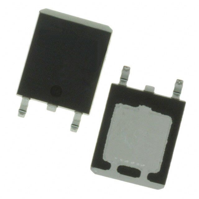
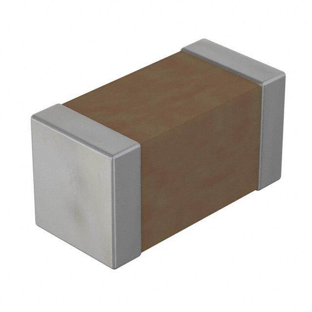
| 描述 | MOSFET N-CH 30V 100A ATPAK |
| 产品分类 | FET - 单 |
| FET功能 | 逻辑电平门 |
| FET类型 | MOSFET N 通道,金属氧化物 |
| 品牌 | ON Semiconductor |
| 数据手册 | |
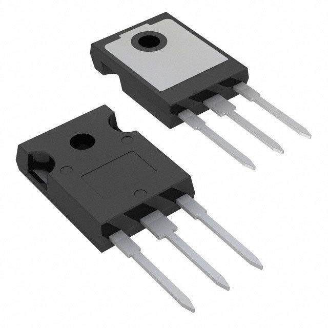
| 产品图片 |
|
| 产品型号 | ATP204-TL-H |
| PCN设计/规格 | |
| rohs | 无铅 / 符合限制有害物质指令(RoHS)规范要求 |
| 产品系列 | - |
| 不同Id时的Vgs(th)(最大值) | - |
| 不同Vds时的输入电容(Ciss) | 4600pF @ 10V |
| 不同Vgs时的栅极电荷(Qg) | 70nC @ 10V |
| 不同 Id、Vgs时的 RdsOn(最大值) | 5.6 毫欧 @ 50A,10V |
| 产品目录绘图 |
|
| 产品目录页面 | |
| 供应商器件封装 | ATPAK |
| 其它名称 | 869-1080-1 |
| 功率-最大值 | 60W |
| 包装 | 剪切带 (CT) |
| 安装类型 | 表面贴装 |
| 封装/外壳 | ATPAK(2 引线 + 接片) |
| 标准包装 | 1 |
| 漏源极电压(Vdss) | 30V |
| 电流-连续漏极(Id)(25°C时) | 100A (Ta) |


- 商务部:美国ITC正式对集成电路等产品启动337调查
- 曝三星4nm工艺存在良率问题 高通将骁龙8 Gen1或转产台积电
- 太阳诱电将投资9.5亿元在常州建新厂生产MLCC 预计2023年完工
- 英特尔发布欧洲新工厂建设计划 深化IDM 2.0 战略
- 台积电先进制程称霸业界 有大客户加持明年业绩稳了
- 达到5530亿美元!SIA预计今年全球半导体销售额将创下新高
- 英特尔拟将自动驾驶子公司Mobileye上市 估值或超500亿美元
- 三星加码芯片和SET,合并消费电子和移动部门,撤换高东真等 CEO
- 三星电子宣布重大人事变动 还合并消费电子和移动部门
- 海关总署:前11个月进口集成电路产品价值2.52万亿元 增长14.8%


PDF Datasheet 数据手册内容提取
Ordering number : ENA1551A ATP204 N-Channel Power MOSFET 30V, 100A, 5.6mΩ, Single ATPAK http://onsemi.com Features • Low ON-resistance • Large current • 4.5V drive • Slim package • Halogen free compliance • Protection diode in Specifi cations Absolute Maximum Ratings at Ta=25°C Parameter Symbol Conditions Ratings Unit Drain-to-Source Voltage VDSS 30 V Gate-to-Source Voltage VGSS ±20 V Drain Current (DC) ID 100 A Drain Current (PW≤10μs) IDP PW≤10μs, duty cycle≤1% 300 A Allowable Power Dissipation PD Tc=25°C 60 W Channel Temperature Tch 150 °C Storage Temperature Tstg --55 to +150 °C Avalanche Energy (Single Pulse) *1 EAS 235 mJ Avalanche Current *2 IAV 50 A Note : *1 VDD=15V, L=100μH, IAV=50A *2 L≤100μH, Single pulse Stresses exceeding Maximum Ratings may damage the device. Maximum Ratings are stress ratings only. Functional operation above the Recommended Operating Conditions is not implied. Extended exposure to stresses above the Recommended Operating Conditions may affect device reliability. Package Dimensions Product & Package Information unit : mm (typ) • Package : ATPAK 7057-001 • JEITA, JEDEC : - • Minimum Packing Quantity : 3,000 pcs./reel ATP204-TL-H 6.5 1.5 4.6 Packing Type: TL Marking 2.6 4 0.5 0.4 0.4 ATP204 LOT No. 5 TL 0 6 6. 7.3 9.5 4. Electrical Connection 2,4 2 5 1 3 1.7 0.55 0. 0.8 0.6 0.7 0.4 1 : Gate 2.3 2.3 2 : Drain 1 3 : Source 4 : Drain 0.1 ATPAK 3 Semiconductor Components Industries, LLC, 2013 July, 2013 61312 TKIM/91609PA TKIM TC-00002081 No. A1551-1/7
ATP204 Electrical Characteristics at Ta=25°C Ratings Parameter Symbol Conditions Unit min typ max Drain-to-Source Breakdown Voltage V(BR)DSS ID=1mA, VGS=0V 30 V Zero-Gate Voltage Drain Current IDSS VDS=30V, VGS=0V 1 μA Gate-to-Source Leakage Current IGSS VGS=±16V, VDS=0V ±10 μA Cutoff Voltage VGS(off) VDS=10V, ID=1mA 1.2 2.6 V Forward Transfer Admittance | yfs | VDS=10V, ID=50A 100 S RDS(on)1 ID=50A, VGS=10V 4.3 5.6 mΩ Static Drain-to-Source On-State Resistance RDS(on)2 ID=25A, VGS=4.5V 6.5 9.1 mΩ Input Capacitance Ciss 4600 pF Output Capacitance Coss VDS=10V, f=1MHz 700 pF Reverse Transfer Capacitance Crss 390 pF Turn-ON Delay Time td(on) 40 ns Rise Time tr 690 ns See specifi ed Test Circuit. Turn-OFF Delay Time td(off) 205 ns Fall Time tf 110 ns Total Gate Charge Qg 70 nC Gate-to-Source Charge Qgs VDS=15V, VGS=10V, ID=100A 22 nC Gate-to-Drain “Miller” Charge Qgd 9.2 nC Diode Forward Voltage VSD IS=100A, VGS=0V 1.03 1.2 V Switching Time Test Circuit VIN VDD=15V 10V 0V ID=50A VIN RL=0.3Ω D VOUT PW=10μs D.C.≤1% G ATP204 P.G 50Ω S Ordering Information Device Package Shipping memo ATP204-TL-H ATPAK 3,000pcs./reel Pb Free and Halogen Free No. A1551-2/7
ATP204 ID -- VDS ID -- VGS 100 150 9800 0V8.0V 6.0V 4.5 V Tc=25°C 111342000 VDS=10V Tc=--25°C75°C 25°C A 10. A 110 ent, I-- D 657000 16.0V 4.0V ent, I-- D 1908000 urr urr 70 C 40 C 60 n n C Drai 3200 VGS=3.5V Drai 543000 Tc=75° 5°C C 2 10 20 25° -- 10 0 0 0 0.2 0.4 0.6 0.8 1.0 1.2 1.4 1.6 1.8 2.0 0 1 2 3 4 5 6 Drain-to-Source Voltage, VDS -- V IT14998 Gate-to-Source Voltage, VGS -- V IT14999 RDS(on) -- VGS RDS(on) -- Tc 14 14 Tc=25°C Single pulse Single pulse Ω Ω m 12 m 12 n) -- ID=25A n) -- 10 (oDS 10 50A (oDS =25A Static Drain-to-SourceOn-State Resistance, R 648 Static Drain-to-SourceOn-State Resistance, R 8462 V VGSG=S4=.51V0., 0IVD, I D=50A 2 0 0 2 4 6 8 10 12 14 16 --60 --40 --20 0 20 40 60 80 100 120 140 160 Gate-to-Source Voltage, VGS -- V IT15000 Case Temperature, Tc -- °C IT15001 | yfs | -- ID IS -- VSD 3 3 2 VDS=10V 2 VGS=0V S 100 Single pulse y ansfer Admittance, fs -- || 11000757532 Tc= --257°5C°2C5°C urce Current, I -- AS 011..10075327575327532 Tc=75°C 25°C--25°C Tr 3 So 3 d 2 2 ar 0.01 w 7 For 1.0 53 7 2 5 0.001 0.1 2 3 5 7 1.0 2 3 5 7 10 2 3 5 7100 0 0.2 0.4 0.6 0.8 1.0 1.2 1.4 Drain Current, ID -- A IT15002 Diode Forward Voltage, VSD -- V IT15003 SW Time -- ID Ciss, Coss, Crss -- VDS 3 10000 VDD=15V f=1MHz 2 7 VGS=10V 5 Ciss ns1000 W Time -- 357 td(off) ss -- pF 32 S 2 Cr Time, 100 tf Coss, 10007 Coss ching 57 tr Ciss, 5 Crss wit 3 td(on) 3 S 2 2 10 100 0.1 2 3 5 7 1.0 2 3 5 7 10 2 3 5 7100 0 5 10 15 20 25 30 Drain Current, ID -- A IT15004 Drain-to-Source Voltage, VDS -- V IT15005 No. A1551-3/7
ATP204 VGS -- Qg A S O 10 7 VDS=15V 5 IDP=300A PW≤10μs -- VS 89 ID=100A A 100237 ID=100A 1ms100μs10μs e Voltage, VG 567 urrent, I-- D 1057235 Othpise raarteiao nis in 10D100Cmm ss ate-to-Sourc 234 Drain C 1.05723 limited by RDS(on). operation G 1 3 Tc=25°C 2 Single pulse 0 0.1 0 10 20 30 40 50 60 70 0.1 2 3 5 7 1.0 2 3 5 7 10 2 3 5 Total Gate Charge, Qg -- nC IT15006 Drain-to-Source Voltage, VDS -- V IT14982 PD -- Tc EAS -- Ta 70 120 W % wer Dissipation, P-- D 53460000 ergy derating factor-- 1086000 Po En 40 ble 20 che a n w a Allo 10 Aval 20 0 0 00 20 40 60 80 100 120 140 160 0 25 50 75 100 125 150 175 Case Temperature, Tc -- °C IT14983 Ambient Temperature, Ta -- °C IT14011 No. A1551-4/7
ATP204 Taping Specifi cation ATP204-TL-H No. A1551-5/7
ATP204 Outline Drawing Land Pattern Example ATP204-TL-H Mass (g) Unit Unit: mm 0.266 mm * For reference 6.5 7 6. 1.5 2 6 1. 2.3 2.3 No. A1551-6/7
ATP204 Note on usage : Since the ATP204 is a MOSFET product, please avoid using this device in the vicinity of highly charged objects. ON Semiconductor and the ON logo are registered trademarks of Semiconductor Components Industries, LLC (SCILLC). SCILLC owns the rights to a number of patents, trademarks, copyrights, trade secrets, and other intellectual property. A listing of SCILLC’s product/patent coverage may be accessed at www.onsemi.com/site/pdf/Patent-Marking.pdf. SCILLC reserves the right to make changes without further notice to any products herein. SCILLC makes no warranty, representation or guarantee regarding the suitability of its products for any particular purpose, nor does SCILLC assume any liability arising out of the application or use of any product or circuit, and specifically disclaims any and all liability, including without limitation special, consequential or incidental damages. “Typical” parameters which may be provided in SCILLC data sheets and/or specifications can and do vary in different applications and actual performance may vary over time. All operating parameters, including “Typicals” must be validated for each customer application by customer’s technical experts. SCILLC does not convey any license under its patent rights nor the rights of others. SCILLC products are not designed, intended, or authorized for use as components in systems intended for surgical implant into the body, or other applications intended to support or sustain life, or for any other application in which the failure of the SCILLC product could create a situation where personal injury or death may occur. Should Buyer purchase or use SCILLC products for any such unintended or unauthorized application, Buyer shall indemnify and hold SCILLC and its officers, employees, subsidiaries, affiliates, and distributors harmless against all claims, costs, damages, and expenses, and reasonable attorney fees arising out of, directly or indirectly, any claim of personal injury or death associated with such unintended or unauthorized use, even if such claim alleges that SCILLC was negligent regarding the design or manufacture of the part. SCILLC is an Equal Opportunity/Affirmative Action Employer. This literature is subject to all applicable copyright laws and is not for resale in any manner. PS No. A1551-7/7