ICGOO在线商城 > 分立半导体产品 > 晶体管 - FET,MOSFET - 单 > ATP202-TL-H

 Datasheet下载
- 型号: ATP202-TL-H
- 制造商: ON Semiconductor
- 库位|库存: xxxx|xxxx
- 要求:
| 数量阶梯 | 香港交货 | 国内含税 |
| +xxxx | $xxxx | ¥xxxx |
查看当月历史价格
查看今年历史价格
ATP202-TL-H产品简介:
ICGOO电子元器件商城为您提供ATP202-TL-H由ON Semiconductor设计生产,在icgoo商城现货销售,并且可以通过原厂、代理商等渠道进行代购。 ATP202-TL-H价格参考。ON SemiconductorATP202-TL-H封装/规格:晶体管 - FET,MOSFET - 单, 表面贴装 N 沟道 30V 50A(Ta) 40W(Tc) ATPAK。您可以下载ATP202-TL-H参考资料、Datasheet数据手册功能说明书,资料中有ATP202-TL-H 详细功能的应用电路图电压和使用方法及教程。
| 参数 | 数值 |
| 产品目录 | |
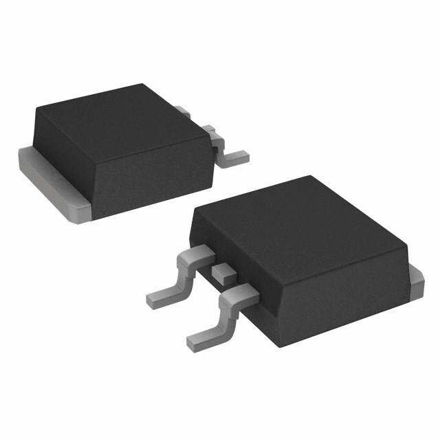
| 描述 | MOSFET N-CH 30V 50A ATPAK |
| 产品分类 | FET - 单 |
| FET功能 | 逻辑电平门 |
| FET类型 | MOSFET N 通道,金属氧化物 |
| 品牌 | ON Semiconductor |
| 数据手册 | |
| 产品图片 |
|
| 产品型号 | ATP202-TL-H |
| PCN组件/产地 | |
| PCN设计/规格 | |
| rohs | 无铅 / 符合限制有害物质指令(RoHS)规范要求 |
| 产品系列 | - |
| 不同Id时的Vgs(th)(最大值) | - |
| 不同Vds时的输入电容(Ciss) | 1650pF @ 10V |
| 不同Vgs时的栅极电荷(Qg) | 27nC @ 10V |
| 不同 Id、Vgs时的 RdsOn(最大值) | 12 毫欧 @ 25A,10V |
| 产品目录绘图 |
|
| 产品目录页面 | |
| 供应商器件封装 | ATPAK |
| 其它名称 | 869-1078-6 |
| 功率-最大值 | 40W |
| 包装 | Digi-Reel® |
| 安装类型 | 表面贴装 |
| 封装/外壳 | ATPAK(2 引线 + 接片) |
| 标准包装 | 1 |
| 漏源极电压(Vdss) | 30V |
| 电流-连续漏极(Id)(25°C时) | 50A (Ta) |


.jpg)


PDF Datasheet 数据手册内容提取
Ordering number : ENA1317A ATP202 N-Channel Power MOSFET 30V, 50A, 12mΩ, Single ATPAK http://onsemi.com Features • Low ON-resistance • Large current • 4.5V drive • Slim package • Halogen free compliance • Protection diode in Specifi cations Absolute Maximum Ratings at Ta=25°C Parameter Symbol Conditions Ratings Unit Drain-to-Source Voltage VDSS 30 V Gate-to-Source Voltage VGSS ±20 V Drain Current (DC) ID 50 A Drain Current (PW≤10μs) IDP PW≤10μs, duty cycle≤1% 150 A Allowable Power Dissipation PD Tc=25°C 40 W Channel Temperature Tch 150 °C Storage Temperature Tstg --55 to +150 °C Avalanche Energy (Single Pulse) *1 EAS 45 mJ Avalanche Current *2 IAV 25 A Note : *1 VDD=10V, L=100μH, IAV=25A *2 L≤100μH, Single pulse Stresses exceeding Maximum Ratings may damage the device. Maximum Ratings are stress ratings only. Functional operation above the Recommended Operating Conditions is not implied. Extended exposure to stresses above the Recommended Operating Conditions may affect device reliability. Package Dimensions Product & Package Information unit : mm (typ) • Package : ATPAK 7057-001 • JEITA, JEDEC : - • Minimum Packing Quantity : 3,000 pcs./reel ATP202-TL-H 6.5 1.5 4.6 Packing Type: TL Marking 2.6 4 0.5 0.4 0.4 ATP202 LOT No. 5 TL 0 6 6. 7.3 9.5 4. Electrical Connection 2,4 2 5 1 3 1.7 0.55 0. 0.8 0.6 0.7 0.4 1 : Gate 2.3 2.3 2 : Drain 1 3 : Source 4 : Drain 0.1 ATPAK 3 Semiconductor Components Industries, LLC, 2013 July, 2013 61312 TKIM/91708PA TIIM TC-00001568 No. A1317-1/7
ATP202 Electrical Characteristics at Ta=25°C Ratings Parameter Symbol Conditions Unit min typ max Drain-to-Source Breakdown Voltage V(BR)DSS ID=1mA, VGS=0V 30 V Zero-Gate Voltage Drain Current IDSS VDS=30V, VGS=0V 1 μA Gate-to-Source Leakage Current IGSS VGS=±16V, VDS=0V ±10 μA Cutoff Voltage VGS(off) VDS=10V, ID=1mA 1.2 2.6 V Forward Transfer Admittance | yfs | VDS=10V, ID=25A 10 17 S RDS(on)1 ID=25A, VGS=10V 9 12 mΩ Static Drain-to-Source On-State Resistance RDS(on)2 ID=13A, VGS=4.5V 14 20 mΩ Input Capacitance Ciss 1650 pF Output Capacitance Coss VDS=10V, f=1MHz 285 pF Reverse Transfer Capacitance Crss 160 pF Turn-ON Delay Time td(on) 16 ns Rise Time tr 185 ns See specifi ed Test Circuit. Turn-OFF Delay Time td(off) 93 ns Fall Time tf 93 ns Total Gate Charge Qg 27 nC Gate-to-Source Charge Qgs VDS=15V, VGS=10V, ID=50A 7.5 nC Gate-to-Drain “Miller” Charge Qgd 4 nC Diode Forward Voltage VSD IS=50A, VGS=0V 0.97 1.2 V Switching Time Test Circuit VIN VDD=15V 10V 0V ID=25A VIN RL=0.6Ω D VOUT PW=10μs D.C.≤1% G ATP202 P.G 50Ω S Ordering Information Device Package Shipping memo ATP202-TL-H ATPAK 3,000pcs./reel Pb Free and Halogen Free No. A1317-2/7
ATP202 ID -- VDS ID -- VGS 70 70 Tc=25°C 0V 8.0V6.0V 4.5 V VDS=10V 25°C 5°C 60 10. 60 = -- 7 Tc C -- AD 50 16.0V 4.0V -- AD 50 25° nt, I 40 nt, I 40 e e urr 30 urr 30 C C Drain 20 VGS=3.5V Drain 20 75°C = C Tc C 10 10 5° 5° 2 2 -- 0 0 0 0.5 1.0 1.5 2.0 0 0.5 1.0 1.5 2.0 2.5 3.0 3.5 4.0 4.5 5.0 Drain-to-Source Voltage, VDS -- V IT14012 Gate-to-Source Voltage, VGS -- V IT14013 RDS(on) -- VGS RDS(on) -- Tc 30 30 Tc=25°C Single pulse Ω Single pulse Ω m 25 m 25 n) -- ID=13A n) -- (oDS 20 25A (oDS 20 =13A Static Drain-to-SourceOn-State Resistance, R 11055 Static Drain-to-SourceOn-State Resistance, R 11505 V GSV=4G.S5=V,1 0I.D0V, I D=25A 0 0 0 2 4 6 8 10 12 14 16 --60 --40 --20 0 20 40 60 80 100 120 140 160 Gate-to-Source Voltage, VGS -- V IT14014 Case Temperature, Tc -- °C IT14015 | yfs | -- ID IS -- VSD 5 100 VDS=10V 57 VGS=0V y Admittance, fs -- S|| 107532 Tc= --257°5C°C 25°C urrent, I -- AS 11.0025732573223 Single pulse Forward Transfer 1.0372 Source C 0.00.1157322573 Tc=75°C 25°C--25°C 5 0.001 0.1 2 3 5 7 1.0 2 3 5 7 10 22 3 5 7100 0.2 0.4 0.6 0.8 1.0 1.2 1.4 Drain Current, ID -- A IT14016 Diode Forward Voltage, VSD -- V IT14017 SW Time -- ID Ciss, Coss, Crss -- VDS 7 5 5 VDD=15V f=1MHz VGS=10V 3 s 3 W Time -- n 1002 td(off) ss -- pF10002 Ciss S 7 Cr 7 me, 5 tf ss, 5 Ti Co ng 3 tr s, 3 Coss witchi 2 td(on) Cis 2 Crss S 10 7 100 5 7 0.1 2 3 5 7 1.0 2 3 5 7 10 2 3 5 7 0 5 10 15 20 25 30 Drain Current, ID -- A IT14018 Drain-to-Source Voltage, VDS -- V IT14019 No. A1317-3/7
ATP202 VGS -- Qg A S O 10 3 VDS=15V 2 IDP=150A PW≤10μs o-Source Voltage, V-- VGS 4635879 ID=50A Drain Current, I-- AD 1110.00023572357 ID=50AOtlhimpisei traeardtei aob nyis iRnDS10(o0mn)s. DC ope1r0a1tmi0o1s0nmμss 10μs ate-t 2 57 G 3 1 2 Tc=25°C Single pulse 0 0.1 0 5 10 15 20 25 30 0.1 2 3 5 7 1.0 2 3 5 7 10 2 3 5 Total Gate Charge, Qg -- nC IT14020 Drain-to-Source Voltage, VDS -- V IT14021 PD -- Tc EAS -- Ta 45 120 W 40 % wer Dissipation, P-- D 33220550 ergy derating factor-- 1086000 Po 15 En 40 able 10 nche w a o al 20 All 5 Av 0 0 0 20 40 60 80 100 120 140 160 0 25 50 75 100 125 150 175 Case Temperature, Tc -- °C IT14022 Ambient Temperature, Ta -- °C IT14011 No. A1317-4/7
ATP202 Taping Specifi cation ATP202-TL-H No. A1317-5/7
ATP202 Outline Drawing Land Pattern Example ATP202-TL-H Mass (g) Unit Unit: mm 0.266 mm * For reference 6.5 7 6. 1.5 2 6 1. 2.3 2.3 No. A1317-6/7
ATP202 Note on usage : Since the ATP202 is a MOSFET product, please avoid using this device in the vicinity of highly charged objects. ON Semiconductor and the ON logo are registered trademarks of Semiconductor Components Industries, LLC (SCILLC). SCILLC owns the rights to a number of patents, trademarks, copyrights, trade secrets, and other intellectual property. A listing of SCILLC’s product/patent coverage may be accessed at www.onsemi.com/site/pdf/Patent-Marking.pdf. SCILLC reserves the right to make changes without further notice to any products herein. SCILLC makes no warranty, representation or guarantee regarding the suitability of its products for any particular purpose, nor does SCILLC assume any liability arising out of the application or use of any product or circuit, and specifically disclaims any and all liability, including without limitation special, consequential or incidental damages. “Typical” parameters which may be provided in SCILLC data sheets and/or specifications can and do vary in different applications and actual performance may vary over time. All operating parameters, including “Typicals” must be validated for each customer application by customer’s technical experts. SCILLC does not convey any license under its patent rights nor the rights of others. SCILLC products are not designed, intended, or authorized for use as components in systems intended for surgical implant into the body, or other applications intended to support or sustain life, or for any other application in which the failure of the SCILLC product could create a situation where personal injury or death may occur. Should Buyer purchase or use SCILLC products for any such unintended or unauthorized application, Buyer shall indemnify and hold SCILLC and its officers, employees, subsidiaries, affiliates, and distributors harmless against all claims, costs, damages, and expenses, and reasonable attorney fees arising out of, directly or indirectly, any claim of personal injury or death associated with such unintended or unauthorized use, even if such claim alleges that SCILLC was negligent regarding the design or manufacture of the part. SCILLC is an Equal Opportunity/Affirmative Action Employer. This literature is subject to all applicable copyright laws and is not for resale in any manner. PS No. A1317-7/7