ICGOO在线商城 > ATMEGA16U4-MUR
- 型号: ATMEGA16U4-MUR
- 制造商: Atmel
- 库位|库存: xxxx|xxxx
- 要求:
| 数量阶梯 | 香港交货 | 国内含税 |
| +xxxx | $xxxx | ¥xxxx |
查看当月历史价格
查看今年历史价格
ATMEGA16U4-MUR产品简介:
ICGOO电子元器件商城为您提供ATMEGA16U4-MUR由Atmel设计生产,在icgoo商城现货销售,并且可以通过原厂、代理商等渠道进行代购。 提供ATMEGA16U4-MUR价格参考以及AtmelATMEGA16U4-MUR封装/规格参数等产品信息。 你可以下载ATMEGA16U4-MUR参考资料、Datasheet数据手册功能说明书, 资料中有ATMEGA16U4-MUR详细功能的应用电路图电压和使用方法及教程。
| 参数 | 数值 |
| 产品目录 | 集成电路 (IC) |
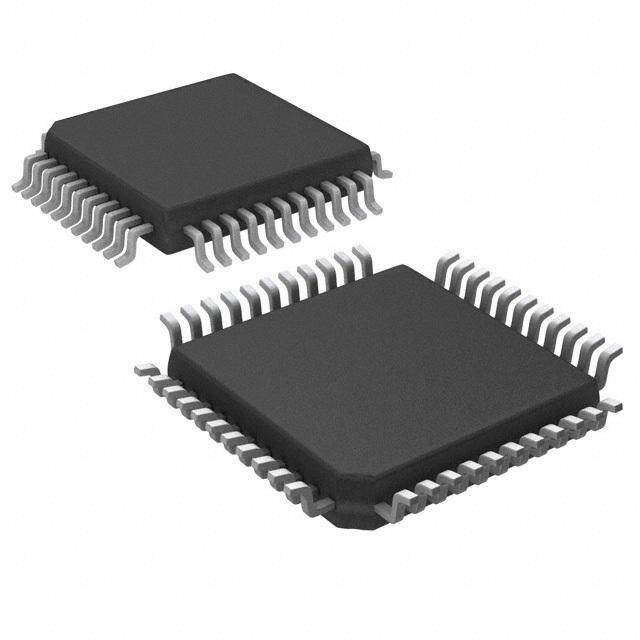
| 描述 | IC MCU 8BIT 16KB FLASH 44QFN |
| EEPROM容量 | 512 x 8 |
| 产品分类 | |
| I/O数 | 26 |
| 品牌 | Atmel |
| 数据手册 | |
| 产品图片 | |
| 产品型号 | ATMEGA16U4-MUR |
| PCN其它 | |
| RAM容量 | 1.25K x 8 |
| rohs | 无铅 / 符合限制有害物质指令(RoHS)规范要求 |
| 产品系列 | AVR® ATmega |
| 产品培训模块 | http://www.digikey.cn/PTM/IndividualPTM.page?site=cn&lang=zhs&ptm=24997http://www.digikey.cn/PTM/IndividualPTM.page?site=cn&lang=zhs&ptm=25692http://www.digikey.cn/PTM/IndividualPTM.page?site=cn&lang=zhs&ptm=26162http://www.digikey.cn/PTM/IndividualPTM.page?site=cn&lang=zhs&ptm=26159http://www.digikey.cn/PTM/IndividualPTM.page?site=cn&lang=zhs&ptm=26180 |
| 供应商器件封装 | 44-QFN(7x7) |
| 其它名称 | ATMEGA16U4-MURDKR |
| 包装 | Digi-Reel® |
| 外设 | 欠压检测/复位,POR,PWM,温度传感器,WDT |
| 封装/外壳 | 44-VFQFN 裸露焊盘 |
| 工作温度 | -40°C ~ 85°C |
| 振荡器类型 | 内部 |
| 数据转换器 | A/D 12x10b |
| 标准包装 | 1 |
| 核心处理器 | AVR |
| 核心尺寸 | 8-位 |
| 电压-电源(Vcc/Vdd) | 2.7 V ~ 5.5 V |
| 程序存储器类型 | 闪存 |
| 程序存储容量 | 16KB(8K x 16) |
| 连接性 | I²C, SPI, UART/USART, USB |
| 速度 | 16MHz |




- 商务部:美国ITC正式对集成电路等产品启动337调查
- 曝三星4nm工艺存在良率问题 高通将骁龙8 Gen1或转产台积电
- 太阳诱电将投资9.5亿元在常州建新厂生产MLCC 预计2023年完工
- 英特尔发布欧洲新工厂建设计划 深化IDM 2.0 战略
- 台积电先进制程称霸业界 有大客户加持明年业绩稳了
- 达到5530亿美元!SIA预计今年全球半导体销售额将创下新高
- 英特尔拟将自动驾驶子公司Mobileye上市 估值或超500亿美元
- 三星加码芯片和SET,合并消费电子和移动部门,撤换高东真等 CEO
- 三星电子宣布重大人事变动 还合并消费电子和移动部门
- 海关总署:前11个月进口集成电路产品价值2.52万亿元 增长14.8%



PDF Datasheet 数据手册内容提取
ATmega16U4/ATmega32U4 8-bit Microcontroller with 16/32K bytes of ISP Flash and USB Controller DATASHEET SUMMARY Features • High Performance, Low Power AVR® 8-Bit Microcontroller • Advanced RISC Architecture – 135 Powerful Instructions – Most Single Clock Cycle Execution – 32 x 8 General Purpose Working Registers – Fully Static Operation – Up to 16 MIPS Throughput at 16MHz – On-Chip 2-cycle Multiplier • Non-volatile Program and Data Memories – 16/32KB of In-System Self-Programmable Flash – 1.25/2.5KB Internal SRAM – 512Bytes/1KB Internal EEPROM – Write/Erase Cycles: 10,000 Flash/100,000 EEPROM – Data retention: 20 years at 85C/ 100 years at 25C(1) – Optional Boot Code Section with Independent Lock Bits In-System Programming by On-chip Boot Program True Read-While-Write Operation Parts using external XTAL clock are pre-programed with a default USB bootloader – Programming Lock for Software Security • JTAG (IEEE® std. 1149.1 compliant) Interface – Boundary-scan Capabilities According to the JTAG Standard – Extensive On-chip Debug Support – Programming of Flash, EEPROM, Fuses, and Lock Bits through the JTAG Interface • USB 2.0 Full-speed/Low Speed Device Module with Interrupt on Transfer Completion – Complies fully with Universal Serial Bus Specification Rev 2.0 – Supports data transfer rates up to 12Mbit/s and 1.5Mbit/s – Endpoint 0 for Control Transfers: up to 64-bytes – Six Programmable Endpoints with IN or Out Directions and with Bulk, Interrupt or Isochronous Transfers – Configurable Endpoints size up to 256 bytes in double bank mode – Fully independent 832 bytes USB DPRAM for endpoint memory allocation – Suspend/Resume Interrupts – CPU Reset possible on USB Bus Reset detection – 48MHz from PLL for Full-speed Bus Operation – USB Bus Connection/Disconnection on Microcontroller Request – Crystal-less operation for Low Speed mode • Peripheral Features – On-chip PLL for USB and High Speed Timer: 32 up to 96MHz operation – One 8-bit Timer/Counter with Separate Prescaler and Compare Mode Atmel-7766JS-USB-ATmega16U4/32U4-Datasheet_04/2016
– Two 16-bit Timer/Counter with Separate Prescaler, Compare- and Capture Mode – One 10-bit High-Speed Timer/Counter with PLL (64MHz) and Compare Mode – Four 8-bit PWM Channels – Four PWM Channels with Programmable Resolution from 2 to 16 Bits – Six PWM Channels for High Speed Operation, with Programmable Resolution from 2 to 11 Bits – Output Compare Modulator – 12-channels, 10-bit ADC (features Differential Channels with Programmable Gain) – Programmable Serial USART with Hardware Flow Control – Master/Slave SPI Serial Interface – Byte Oriented 2-wire Serial Interface – Programmable Watchdog Timer with Separate On-chip Oscillator – On-chip Analog Comparator – Interrupt and Wake-up on Pin Change – On-chip Temperature Sensor • Special Microcontroller Features – Power-on Reset and Programmable Brown-out Detection – Internal 8MHz Calibrated Oscillator – Internal clock prescaler and On-the-fly Clock Switching (Int RC / Ext Osc) – External and Internal Interrupt Sources – Six Sleep Modes: Idle, ADC Noise Reduction, Power-save, Power-down, Standby, and Extended Standby • I/O and Packages – All I/O combine CMOS outputs and LVTTL inputs – 26 Programmable I/O Lines – 44-lead TQFP Package, 10x10mm – 44-lead QFN Package, 7x7mm • Operating Voltages – 2.7 - 5.5V • Operating temperature – Industrial (-40°C to +85°C) • Maximum Frequency – 8MHz at 2.7V - Industrial range – 16MHz at 4.5V - Industrial range Note: 1. See “Data Retention” on page8 for details. 2 ATmega16U4/32U4 [DATASHEET] Atmel-7766JS-USB-ATmega16U4/32U4-Datasheet_04/2016
1. Pin Configurations Figure 1-1. Pinout CK) MS) DO) DI) T T T T 0) 1) 4/ 5/ 6/ 7/ C C C C C C D D D D D D AVCC GND AREF PF0 (A PF1 (A PF4 (A PF5 (A PF6 (A PF7 (A GND VCC 4 3 2 1 0 9 8 7 6 5 4 4 4 4 4 4 3 3 3 3 3 3 (INT.6/AIN0) PE6 1 33 PE2 (HWB) UVcc 2 32 PC7 (ICP3/CLK0/OC)4A INDEX CORNER D- 3 31 PC6 O( C3A/OC4A) D+ 4 30 PB6 (PCINT6/OC1B/OC4B/ADC UGnd 5 29 PB5 (PCINT5/OC1A/OC4B/ADC UCap 6 ATmega32U4 28 PB4 (PCINT4/ADC11) ATmega16U4 VBus 7 27 PD7 (T0/OC4D/ADC10) 44-pin QFN/QTFP (SS/PCINT0) PB0 8 26 PD6 (T1/OC4D/ADC9) (PCINT1/SCL) KPB1 9 25 PD4 (ICP1/ADC8) (PDI/PCINT2/MOSI) PB2 10 24 AVCC (PDO/PCINT3/MIS)O PB3 11 23 GND 2 3 4 5 6 7 8 9 0 1 2 1 1 1 1 1 1 1 1 2 2 2 C D 2 1 C1C/RTS) PB7 RESET VC GN XTAL XTAL SCL/INT0) PD0 (SDA/INT1) PD1 RXD1/INT2) PD2 TXD1/INT3) PD3 XCK1/CTS) PD5 O B/ ( ( ( A/ C0 0 O C ( O 7/ T N CI P ( 2. Overview The ATmega16U4/ATmega32U4 is a low-power CMOS 8-bit microcontroller based on the AVR enhanced RISC architecture. By executing powerful instructions in a single clock cycle, the device achieves throughputs approaching 1 MIPS per MHz allowing the system designer to optimize power consumption versus processing speed. ATmega16U4/32U4 [DATASHEET ] 3 Atmel-7766JS-USB-ATmega16U4/32U4-Datasheet_04/2016
2.1 Block Diagram Figure 2-1. Block Diagram PF7 - PF4 PF1 PF0 PC7PC6 XTAL1 XTAL2 RESET VCC PORTF DRIVERS PORTC DRIVERS GND DATAREGISTER DATADIR. DATAREGISTER DATADIR. PORTF REG.PORTF PORTC REG.PORTC 8-BIT DATA BUS POR - BOD RESET OISNCTIELRLANTAOLR CALIB. OSC OSCILLATOR WATCHDOG JTAG TAP PCROOUGNRTAEMR PSOTINACTEKR TIMER ON-CHIP DEBUG PRFOLAGSRHAM SRAM MCRUE GCOISNTTERROL TCIMOINNTGR AONLD BOUSNCDAANRY- INRSETGRUISCTTEIRON PGUERNPEORSAEL COTIUMNETRESR/S REGISTERS INTERRUPT X UNIT UVcc PROGLORAGMICMING INDSETRCUOCDTEIRON YZ EEPROM USOBN -PCAHDI P3V REGULATOR UCap TEMPERATURE SENSOR COLNINTERSOL ALU 1uF AVCC HIGH SPEED PLL ADC TIMER/PWM AGND STATUS REGISTER VBUS AREF DP USB 2.0 DM ANALOG TWO-WIRE SERIAL COMPARATOR USART1 SPI INTERFACE DATAREGISTER DATADIR. DATAREGISTER DATADIR. DATAREGISTER DATADIR. PORTE REG.PORTE PORTB REG.PORTB PORTD REG.PORTD PORTE DRIVERS PORTB DRIVERS PORTD DRIVERS PE6 PE2 PB7 - PB0 PD7 - PD0 The AVR core combines a rich instruction set with 32 general purpose working registers. All the 32 registers are directly connected to the Arithmetic Logic Unit (ALU), allowing two independent registers to be accessed in one single instruction executed in one clock cycle. The resulting architecture is more code efficient while achieving throughputs up to ten times faster than conventional CISC microcontrollers. The device provides the following features: 16/32K bytes of In-System Programmable Flash with Read-While- Write capabilities, 512Bytes/1K bytes EEPROM, 1.25/2.5K bytes SRAM, 26 general purpose I/O lines (CMOS outputs and LVTTL inputs), 32 general purpose working registers, four flexible Timer/Counters with compare modes and PWM, one more high-speed Timer/Counter with compare modes and PLL adjustable source, one USART (including CTS/RTS flow control signals), a byte oriented 2-wire Serial Interface, a 12-channels 10-bit ADC with optional differential input stage with programmable gain, an on-chip calibrated temperature sensor, a programmable Watchdog Timer with Internal Oscillator, an SPI serial port, IEEE std. 1149.1 compliant JTAG test interface, also used for accessing the On-chip Debug system and programming and six software selectable 4 ATmega16U4/32U4 [DATASHEET] Atmel-7766JS-USB-ATmega16U4/32U4-Datasheet_04/2016
power saving modes. The Idle mode stops the CPU while allowing the SRAM, Timer/Counters, SPI port, and interrupt system to continue functioning. The Power-down mode saves the register contents but freezes the Oscillator, disabling all other chip functions until the next interrupt or Hardware Reset. The ADC Noise Reduction mode stops the CPU and all I/O modules except ADC, to minimize switching noise during ADC conversions. In Standby mode, the Crystal/Resonator Oscillator is running while the rest of the device is sleeping. This allows very fast start-up combined with low power consumption. The device is manufactured using the Atmel® high-density nonvolatile memory technology. The On-chip ISP Flash allows the program memory to be reprogrammed in-system through an SPI serial interface, by a conventional nonvolatile memory programmer, or by an On-chip Boot program running on the AVR core. The boot program can use any interface to download the application program in the application Flash memory. Software in the Boot Flash section will continue to run while the Application Flash section is updated, providing true Read-While-Write operation. By combining an 8-bit RISC CPU with In-System Self-Programmable Flash on a monolithic chip, the device is a powerful microcontroller that provides a highly flexible and cost effective solution to many embedded control applications. The ATmega16U4/ATmega32U4 AVR is supported with a full suite of program and system development tools including: C compilers, macro assemblers, program debugger/simulators, in-circuit emulators, and evaluation kits. 2.2 Pin Descriptions 2.2.1 VCC Digital supply voltage. 2.2.2 GND Ground. 2.2.3 Port B (PB7..PB0) Port B is an 8-bit bi-directional I/O port with internal pull-up resistors (selected for each bit). The Port B output buffers have symmetrical drive characteristics with both high sink and source capability. As inputs, Port B pins that are externally pulled low will source current if the pull-up resistors are activated. The Port B pins are tri- stated when a reset condition becomes active, even if the clock is not running. Port B has better driving capabilities than the other ports. Port B also serves the functions of various special features of the device as listed on page74. 2.2.4 Port C (PC7,PC6) Port C is an 8-bit bi-directional I/O port with internal pull-up resistors (selected for each bit). The Port C output buffers have symmetrical drive characteristics with both high sink and source capability. As inputs, Port C pins that are externally pulled low will source current if the pull-up resistors are activated. The Port C pins are tri- stated when a reset condition becomes active, even if the clock is not running. Only bits 6 and 7 are present on the product pinout. Port C also serves the functions of special features of the device as listed on page77. 2.2.5 Port D (PD7..PD0) Port D is an 8-bit bi-directional I/O port with internal pull-up resistors (selected for each bit). The Port D output buffers have symmetrical drive characteristics with both high sink and source capability. As inputs, Port D pins that are externally pulled low will source current if the pull-up resistors are activated. The Port D pins are tri- stated when a reset condition becomes active, even if the clock is not running. ATmega16U4/32U4 [DATASHEET ] 5 Atmel-7766JS-USB-ATmega16U4/32U4-Datasheet_04/2016
Port D also serves the functions of various special features of the ATmega16U4/ATmega32U4 as listed on page78. 2.2.6 Port E (PE6,PE2) Port E is an 8-bit bi-directional I/O port with internal pull-up resistors (selected for each bit). The Port E output buffers have symmetrical drive characteristics with both high sink and source capability. As inputs, Port E pins that are externally pulled low will source current if the pull-up resistors are activated. The Port E pins are tri- stated when a reset condition becomes active, even if the clock is not running. Only bits 2 and 6 are present on the product pinout. Port E also serves the functions of various special features of the ATmega16U4/ATmega32U4 as listed on page81. 2.2.7 Port F (PF7..PF4, PF1,PF0) Port F serves as analog inputs to the A/D Converter. Port F also serves as an 8-bit bi-directional I/O port, if the A/D Converter channels are not used. Port pins can provide internal pull-up resistors (selected for each bit). The Port F output buffers have symmetrical drive characteristics with both high sink and source capability. As inputs, Port F pins that are externally pulled low will source current if the pull-up resistors are activated. The Port F pins are tri-stated when a reset condition becomes active, even if the clock is not running. Bits 2 and 3 are not present on the product pinout. Port F also serves the functions of the JTAG interface. If the JTAG interface is enabled, the pull-up resistors on pins PF7(TDI), PF5(TMS), and PF4(TCK) will be activated even if a reset occurs. 2.2.8 D- USB Full speed / Low Speed Negative Data Upstream Port. Should be connected to the USB D- connector pin with a serial 22 resistor. 2.2.9 D+ USB Full speed / Low Speed Positive Data Upstream Port. Should be connected to the USB D+ connector pin with a serial 22 resistor. 2.2.10 UGND USB Pads Ground. 2.2.11 UVCC USB Pads Internal Regulator Input supply voltage. 2.2.12 UCAP USB Pads Internal Regulator Output supply voltage. Should be connected to an external capacitor (1µF). 2.2.13 VBUS USB VBUS monitor input. 6 ATmega16U4/32U4 [DATASHEET] Atmel-7766JS-USB-ATmega16U4/32U4-Datasheet_04/2016
2.2.14 RESET Reset input. A low level on this pin for longer than the minimum pulse length will generate a reset, even if the clock is not running. The minimum pulse length is given in Table8-2 on page53. Shorter pulses are not guaranteed to generate a reset. 2.2.15 XTAL1 Input to the inverting Oscillator amplifier and input to the internal clock operating circuit. 2.2.16 XTAL2 Output from the inverting Oscillator amplifier. 2.2.17 AVCC AVCC is the supply voltage pin (input) for all the A/D Converter channels. If the ADC is not used, it should be externally connected to V . If the ADC is used, it should be connected to V through a low-pass filter. CC CC 2.2.18 AREF This is the analog reference pin (input) for the A/D Converter. ATmega16U4/32U4 [DATASHEET ] 7 Atmel-7766JS-USB-ATmega16U4/32U4-Datasheet_04/2016
3. About 3.1 Disclaimer Typical values contained in this datasheet are based on simulations and characterization of other AVR microcontrollers manufactured on the same process technology. Min. and Max. values will be available after the device is characterized. 3.2 Resources A comprehensive set of development tools, application notes and datasheets are available for download on http://www.atmel.com/avr. 3.3 Code Examples This documentation contains simple code examples that briefly show how to use various parts of the device. Be aware that not all C compiler vendors include bit definitions in the header files and interrupt handling in C is compiler dependent. Confirm with the C compiler documentation for more details. These code examples assume that the part specific header file is included before compilation. For I/O registers located in extended I/O map, "IN", "OUT", "SBIS", "SBIC", "CBI", and "SBI" instructions must be replaced with instructions that allow access to extended I/O. Typically "LDS" and "STS" combined with "SBRS", "SBRC", "SBR", and "CBR". 3.4 Data Retention Reliability Qualification results show that the projected data retention failure rate is much less than 1PPM over 20 years at 85°C or 100 years at 25°C. 8 ATmega16U4/32U4 [DATASHEET] Atmel-7766JS-USB-ATmega16U4/32U4-Datasheet_04/2016
4. Register Summary Address Name Bit 7 Bit 6 Bit 5 Bit 4 Bit 3 Bit 2 Bit 1 Bit 0 Page (0xFF) Reserved - - - - - - - - (0xFE) Reserved - - - - - - - - (0xFD) Reserved - - - - - - - - (0xFC) Reserved - - - - - - - - (0xFB) Reserved - - - - - - - - (0xFA) Reserved - - - - - - - - (0xF9) Reserved - - - - (0xF8) Reserved - - - - - - - - (0xF7) Reserved - - - - - - - - (0xF6) Reserved - - - - - - - - (0xF5) Reserved - - - - - - - - (0xF4) UEINT - EPINT6:0 (0xF3) UEBCHX - - - - - BYCT10:8 (0xF2) UEBCLX BYCT7:0 (0xF1) UEDATX DAT7:0 (0xF0) UEIENX FLERRE NAKINE - NAKOUTE RXSTPE RXOUTE STALLEDE TXINE (0xEF) UESTA1X - - - - - CTRLDIR CURRBK1:0 (0xEE) UESTA0X CFGOK OVERFI UNDERFI - DTSEQ1:0 NBUSYBK1:0 (0xED) UECFG1X EPSIZE2:0 EPBK1:0 ALLOC - (0xEC) UECFG0X EPTYPE1:0 - - - - - EPDIR (0xEB) UECONX - - STALLRQ STALLRQC RSTDT - - EPEN (0xEA) UERST - EPRST6:0 (0xE9) UENUM - - - - - EPNUM2:0 (0xE8) UEINTX FIFOCON NAKINI RWAL NAKOUTI RXSTPI RXOUTI STALLEDI TXINI (0xE7) Reserved - - - - (0xE6) UDMFN - - - FNCERR - - - - (0xE5) UDFNUMH - - - - - FNUM10:8 (0xE4) UDFNUML FNUM7:0 (0xE3) UDADDR ADDEN UADD6:0 (0xE2) UDIEN - UPRSME EORSME WAKEUPE EORSTE SOFE MSOFE SUSPE (0xE1) UDINT - UPRSMI EORSMI WAKEUPI EORSTI SOFI MSOFI SUSPI (0xE0) UDCON - - - - RSTCPU LSM RMWKUP DETACH (0xDF) Reserved (0xDE) Reserved (0xDD) Reserved (0xDC) Reserved (0xDB) Reserved (0xDA) USBINT - - - - - - - VBUSTI (0xD9) USBSTA - - - - - - ID VBUS (0xD8) USBCON USBE - FRZCLK OTGPADE - - - VBUSTE (0xD7) UHWCON - - - - - - - UVREGE (0xD6) Reserved (0xD5) Reserved (0xD4) DT4 DT4H3 DT4H2 DT4H1 DT4H0 DT4L3 DT4L2 DT4L1 DT4L0 (0xD3) Reserved (0xD2) OCR4D Timer/Counter4 - Output Compare Register D (0xD1) OCR4C Timer/Counter4 - Output Compare Register C (0xD0) OCR4B Timer/Counter4 - Output Compare Register B (0xCF) OCR4A Timer/Counter4 - Output Compare Register A (0xCE) UDR1 USART1 I/O Data Register (0xCD) UBRR1H - - - - USART1 Baud Rate Register High Byte (0xCC) UBRR1L USART1 Baud Rate Register Low Byte (0xCB) UCSR1D - - - - - - CTSEN RTSEN (0xCA) UCSR1C UMSEL11 UMSEL10 UPM11 UPM10 USBS1 UCSZ11 UCSZ10 UCPOL1 (0xC9) UCSR1B RXCIE1 TXCIE1 UDRIE1 RXEN1 TXEN1 UCSZ12 RXB81 TXB81 (0xC8) UCSR1A RXC1 TXC1 UDRE1 FE1 DOR1 PE1 U2X1 MPCM1 (0xC7) CLKSTA - - - - - - RCON EXTON (0xC6) CLKSEL1 RCCKSEL3 RCCKSEL2 RCCKSEL1 RCCKSEL0 EXCKSEL3 EXCKSEL2 EXCKSEL1 EXCKSEL0 (0xC5) CLKSEL0 RCSUT1 RCSUT0 EXSUT1 EXSUT0 RCE EXTE - CLKS (0xC4) TCCR4E TLOCK4 ENHC4 OC4OE5 OC4OE4 OC4OE3 OC4OE2 OC4OE1 OC4OE0 (0xC3) TCCR4D FPIE4 FPEN4 FPNC4 FPES4 FPAC4 FPF4 WGM41 WGM40 (0xC2) TCCR4C COM4A1S COM4A0S COM4B1S COM4B0S COM4D1S COM4D0S FOC4D PWM4D (0xC1) TCCR4B PWM4X PSR4 DTPS41 DTPS40 CS43 CS42 CS41 CS40 (0xC0) TCCR4A COM4A1 COM4A0 COM4B1 COM4B0 FOC4A FOC4B PWM4A PWM4B (0xBF) TC4H - - - - - Timer/Counter4 High Byte ATmega16U4/32U4 [DATASHEET SUMMARY] 9 Atmel-7766JS-USB-ATmega16U4/32U4-Datasheet_04/2016
Address Name Bit 7 Bit 6 Bit 5 Bit 4 Bit 3 Bit 2 Bit 1 Bit 0 Page (0xBE) TCNT4 Timer/Counter4 - Counter Register Low Byte (0xBD) TWAMR TWAM6 TWAM5 TWAM4 TWAM3 TWAM2 TWAM1 TWAM0 - (0xBC) TWCR TWINT TWEA TWSTA TWSTO TWWC TWEN - TWIE (0xBB) TWDR 2-wire Serial Interface Data Register (0xBA) TWAR TWA6 TWA5 TWA4 TWA3 TWA2 TWA1 TWA0 TWGCE (0xB9) TWSR TWS7 TWS6 TWS5 TWS4 TWS3 - TWPS1 TWPS0 (0xB8) TWBR 2-wire Serial Interface Bit Rate Register (0xB7) Reserved - - - - - - - - (0xB6) Reserved - (0xB5) Reserved - - - - - - - - (0xB4) Reserved - - - - - - - - (0xB3) Reserved - - - - - - - - (0xB2) Reserved - - - - - - - - (0xB1) Reserved - - - - - - - - (0xB0) Reserved - - - - - - - - (0xAF) Reserved - - - - - - - - (0xAE) Reserved - - - - - - - - (0xAD) Reserved - - - - - - - - (0xAC) Reserved - - - - - - - - (0xAB) Reserved - - - - - - - - (0xAA) Reserved - - - - - - - - (0xA9) Reserved - - - - - - - - (0xA8) Reserved - - - - - - - - (0xA7) Reserved - - - - - - - - (0xA6) Reserved - - - - - - - - (0xA5) Reserved - - - - - - - - (0xA4) Reserved - - - - - - - - (0xA3) Reserved - - - - - - - - (0xA2) Reserved - - - - - - - - (0xA1) Reserved - - - - - - - - (0xA0) Reserved - - - - - - - - (0x9F) Reserved - - - - - - - - (0x9E) Reserved - - - - - - - - (0x9D) OCR3CH Timer/Counter3 - Output Compare Register C High Byte (0x9C) OCR3CL Timer/Counter3 - Output Compare Register C Low Byte (0x9B) OCR3BH Timer/Counter3 - Output Compare Register B High Byte (0x9A) OCR3BL Timer/Counter3 - Output Compare Register B Low Byte (0x99) OCR3AH Timer/Counter3 - Output Compare Register A High Byte (0x98) OCR3AL Timer/Counter3 - Output Compare Register A Low Byte (0x97) ICR3H Timer/Counter3 - Input Capture Register High Byte (0x96) ICR3L Timer/Counter3 - Input Capture Register Low Byte (0x95) TCNT3H Timer/Counter3 - Counter Register High Byte (0x94) TCNT3L Timer/Counter3 - Counter Register Low Byte (0x93) Reserved - - - - - - - - (0x92) TCCR3C FOC3A - - - - - - - (0x91) TCCR3B ICNC3 ICES3 - WGM33 WGM32 CS32 CS31 CS30 (0x90) TCCR3A COM3A1 COM3A0 COM3B1 COM3B0 COM3C1 COM3C0 WGM31 WGM30 (0x8F) Reserved - - - - - - - - (0x8E) Reserved - - - - - - - - (0x8D) OCR1CH Timer/Counter1 - Output Compare Register C High Byte (0x8C) OCR1CL Timer/Counter1 - Output Compare Register C Low Byte (0x8B) OCR1BH Timer/Counter1 - Output Compare Register B High Byte (0x8A) OCR1BL Timer/Counter1 - Output Compare Register B Low Byte (0x89) OCR1AH Timer/Counter1 - Output Compare Register A High Byte (0x88) OCR1AL Timer/Counter1 - Output Compare Register A Low Byte (0x87) ICR1H Timer/Counter1 - Input Capture Register High Byte (0x86) ICR1L Timer/Counter1 - Input Capture Register Low Byte (0x85) TCNT1H Timer/Counter1 - Counter Register High Byte (0x84) TCNT1L Timer/Counter1 - Counter Register Low Byte (0x83) Reserved - - - - - - - - (0x82) TCCR1C FOC1A FOC1B FOC1C - - - - - (0x81) TCCR1B ICNC1 ICES1 - WGM13 WGM12 CS12 CS11 CS10 (0x80) TCCR1A COM1A1 COM1A0 COM1B1 COM1B0 COM1C1 COM1C0 WGM11 WGM10 (0x7F) DIDR1 - - - - - - - AIN0D (0x7E) DIDR0 ADC7D ADC6D ADC5D ADC4D - - ADC1D ADC0D (0x7D) DIDR2 - - ADC13D ADC12D ADC11D ADC10D ADC9D ADC8D (0x7C) ADMUX REFS1 REFS0 ADLAR MUX4 MUX3 MUX2 MUX1 MUX0 (0x7B) ADCSRB ADHSM ACME MUX5 - ADTS3 ADTS2 ADTS1 ADTS0 ATmega16U4/32U4 [DATASHEET SUMMARY] 10 Atmel-7766JS-USB-ATmega16U4/32U4-Datasheet_04/2016
Address Name Bit 7 Bit 6 Bit 5 Bit 4 Bit 3 Bit 2 Bit 1 Bit 0 Page (0x7A) ADCSRA ADEN ADSC ADATE ADIF ADIE ADPS2 ADPS1 ADPS0 (0x79) ADCH ADC Data Register High byte (0x78) ADCL ADC Data Register Low byte (0x77) Reserved - - - - - - - - (0x76) Reserved - - - - - - - - (0x75) Reserved - - - - - - - - (0x74) Reserved - - - - - - - - (0x73) Reserved - - - - - - - - (0x72) TIMSK4 OCIE4D OCIE4A OCIE4B - - TOIE4 - - (0x71) TIMSK3 - - ICIE3 - OCIE3C OCIE3B OCIE3A TOIE3 (0x70) Reserved - - - - - - - - (0x6F) TIMSK1 - - ICIE1 - OCIE1C OCIE1B OCIE1A TOIE1 (0x6E) TIMSK0 - - - - - OCIE0B OCIE0A TOIE0 (0x6D) Reserved - - - - - - - - (0x6C) Reserved - - - - - - - - (0x6B) PCMSK0 PCINT7 PCINT6 PCINT5 PCINT4 PCINT3 PCINT2 PCINT1 PCINT0 (0x6A) EICRB - - ISC61 ISC60 - - - - (0x69) EICRA ISC31 ISC30 ISC21 ISC20 ISC11 ISC10 ISC01 ISC00 (0x68) PCICR - - - - - - - PCIE0 (0x67) RCCTRL - - - - - - - RCFREQ (0x66) OSCCAL RC Oscillator Calibration Register (0x65) PRR1 PRUSB - - PRTIM4 PRTIM3 - - PRUSART1 (0x64) PRR0 PRTWI - PRTIM0 - PRTIM1 PRSPI - PRADC (0x63) Reserved - - - - - - - - (0x62) Reserved - - - - - - - - (0x61) CLKPR CLKPCE - - - CLKPS3 CLKPS2 CLKPS1 CLKPS0 (0x60) WDTCSR WDIF WDIE WDP3 WDCE WDE WDP2 WDP1 WDP0 0x3F (0x5F) SREG I T H S V N Z C 0x3E (0x5E) SPH SP15 SP14 SP13 SP12 SP11 SP10 SP9 SP8 0x3D (0x5D) SPL SP7 SP6 SP5 SP4 SP3 SP2 SP1 SP0 0x3C (0x5C) Reserved - - - - - - - - 0x3B (0x5B) RAMPZ - - - - - - RAMPZ1 RAMPZ0 0x3A (0x5A) Reserved - - - - - - - - 0x39 (0x59) Reserved - - - - - - - - 0x38 (0x58) Reserved - - - - - - - - 0x37 (0x57) SPMCSR SPMIE RWWSB SIGRD RWWSRE BLBSET PGWRT PGERS SPMEN 0x36 (0x56) Reserved - - - - - - - - 0x35 (0x55) MCUCR JTD - - PUD - - IVSEL IVCE 0x34 (0x54) MCUSR - - USBRF JTRF WDRF BORF EXTRF PORF 0x33 (0x53) SMCR - - - - SM2 SM1 SM0 SE 0x32 (0x52) PLLFRQ PINMUX PLLUSB PLLTM1 PLLTM0 PDIV3 PDIV2 PDIV1 PDIV0 OCDR/ OCDR7 OCDR6 OCDR5 OCDR4 OCDR3 OCDR2 OCDR1 OCDR0 0x31 (0x51) MONDR Monitor Data Register 0x30 (0x50) ACSR ACD ACBG ACO ACI ACIE ACIC ACIS1 ACIS0 0x2F (0x4F) Reserved - - - - - - - - 0x2E (0x4E) SPDR SPI Data Register 0x2D (0x4D) SPSR SPIF WCOL - - - - - SPI2X 0x2C (0x4C) SPCR SPIE SPE DORD MSTR CPOL CPHA SPR1 SPR0 0x2B (0x4B) GPIOR2 General Purpose I/O Register 2 0x2A (0x4A) GPIOR1 General Purpose I/O Register 1 0x29 (0x49) PLLCSR - - - PINDIV - - PLLE PLOCK 0x28 (0x48) OCR0B Timer/Counter0 Output Compare Register B 0x27 (0x47) OCR0A Timer/Counter0 Output Compare Register A 0x26 (0x46) TCNT0 Timer/Counter0 (8 Bit) 0x25 (0x45) TCCR0B FOC0A FOC0B - - WGM02 CS02 CS01 CS00 0x24 (0x44) TCCR0A COM0A1 COM0A0 COM0B1 COM0B0 - - WGM01 WGM00 0x23 (0x43) GTCCR TSM - - - - - PSRASY PSRSYNC 0x22 (0x42) EEARH - - - - EEPROM Address Register High Byte 0x21 (0x41) EEARL EEPROM Address Register Low Byte 0x20 (0x40) EEDR EEPROM Data Register 0x1F (0x3F) EECR - - EEPM1 EEPM0 EERIE EEMPE EEPE EERE 0x1E (0x3E) GPIOR0 General Purpose I/O Register 0 0x1D (0x3D) EIMSK - INT6 - - INT3 INT2 INT1 INT0 0x1C (0x3C) EIFR - INTF6 - - INTF3 INTF2 INTF1 INTF0 0x1B (0x3B) PCIFR - - - - - - - PCIF0 0x1A (0x3A) Reserved - - - - - - - - 0x19 (0x39) TIFR4 OCF4D OCF4A OCF4B - - TOV4 - - 0x18 (0x38) TIFR3 - - ICF3 - OCF3C OCF3B OCF3A TOV3 ATmega16U4/32U4 [DATASHEET SUMMARY] 11 Atmel-7766JS-USB-ATmega16U4/32U4-Datasheet_04/2016
Address Name Bit 7 Bit 6 Bit 5 Bit 4 Bit 3 Bit 2 Bit 1 Bit 0 Page 0x17 (0x37) Reserved - - - - - - - - 0x16 (0x36) TIFR1 - - ICF1 - OCF1C OCF1B OCF1A TOV1 0x15 (0x35) TIFR0 - - - - - OCF0B OCF0A TOV0 0x14 (0x34) Reserved - - - - - - - - 0x13 (0x33) Reserved - - - - - - - - 0x12 (0x32) Reserved - - - - - - - - 0x11 (0x31) PORTF PORTF7 PORTF6 PORTF5 PORTF4 - - PORTF1 PORTF0 0x10 (0x30) DDRF DDF7 DDF6 DDF5 DDF4 - - DDF1 DDF0 0x0F (0x2F) PINF PINF7 PINF6 PINF5 PINF4 - - PINF1 PINF0 0x0E (0x2E) PORTE - PORTE6 - - - PORTE2 - - 0x0D (0x2D) DDRE - DDE6 - - - DDE2 - - 0x0C (0x2C) PINE - PINE6 - - - PINE2 - - 0x0B (0x2B) PORTD PORTD7 PORTD6 PORTD5 PORTD4 PORTD3 PORTD2 PORTD1 PORTD0 0x0A (0x2A) DDRD DDD7 DDD6 DDD5 DDD4 DDD3 DDD2 DDD1 DDD0 0x09 (0x29) PIND PIND7 PIND6 PIND5 PIND4 PIND3 PIND2 PIND1 PIND0 0x08 (0x28) PORTC PORTC7 PORTC6 - - - - - - 0x07 (0x27) DDRC DDC7 DDC6 - - - - - - 0x06 (0x26) PINC PINC7 PINC6 - - - - - - 0x05 (0x25) PORTB PORTB7 PORTB6 PORTB5 PORTB4 PORTB3 PORTB2 PORTB1 PORTB0 0x04 (0x24) DDRB DDB7 DDB6 DDB5 DDB4 DDB3 DDB2 DDB1 DDB0 0x03 (0x23) PINB PINB7 PINB6 PINB5 PINB4 PINB3 PINB2 PINB1 PINB0 0x02 (0x22) Reserved - - - - - - - - 0x01 (0x21) Reserved - - - - - - - - 0x00 (0x20) Reserved - - - - - - - - Note: 1. For compatibility with future devices, reserved bits should be written to zero if accessed. Reserved I/O memory addresses should never be written. 2. I/O registers within the address range $00 - $1F are directly bit-accessible using the SBI and CBI instructions. In these registers, the value of single bits can be checked by using the SBIS and SBIC instructions. 3. Some of the status flags are cleared by writing a logical one to them. Note that the CBI and SBI instructions will operate on all bits in the I/O register, writing a one back into any flag read as set, thus clearing the flag. The CBI and SBI instruc- tions work with registers 0x00 to 0x1F only. 4. When using the I/O specific commands IN and OUT, the I/O addresses $00 - $3F must be used. When addressing I/O registers as data space using LD and ST instructions, $20 must be added to these addresses. The ATmega16U4/ATmega32U4 is a complex microcontroller with more peripheral units than can be supported within the 64 location reserved in Opcode for the IN and OUT instructions. For the Extended I/O space from $60 - $1FF in SRAM, only the ST/STS/STD and LD/LDS/LDD instructions can be used. ATmega16U4/32U4 [DATASHEET SUMMARY] 12 Atmel-7766JS-USB-ATmega16U4/32U4-Datasheet_04/2016
5. Instruction Set Summary Mnemonics Operands Description Operation Flags #Clocks ARITHMETIC AND LOGIC INSTRUCTIONS ADD Rd, Rr Add two Registers Rd Rd + Rr Z,C,N,V,H 1 ADC Rd, Rr Add with Carry two Registers Rd Rd + Rr + C Z,C,N,V,H 1 ADIW Rdl,K Add Immediate to Word Rdh:Rdl Rdh:Rdl + K Z,C,N,V,S 2 SUB Rd, Rr Subtract two Registers Rd Rd - Rr Z,C,N,V,H 1 SUBI Rd, K Subtract Constant from Register Rd Rd - K Z,C,N,V,H 1 SBC Rd, Rr Subtract with Carry two Registers Rd Rd - Rr - C Z,C,N,V,H 1 SBCI Rd, K Subtract with Carry Constant from Reg. Rd Rd - K - C Z,C,N,V,H 1 SBIW Rdl,K Subtract Immediate from Word Rdh:Rdl Rdh:Rdl - K Z,C,N,V,S 2 AND Rd, Rr Logical AND Registers Rd Rd Rr Z,N,V 1 ANDI Rd, K Logical AND Register and Constant Rd Rd K Z,N,V 1 OR Rd, Rr Logical OR Registers Rd Rd v Rr Z,N,V 1 ORI Rd, K Logical OR Register and Constant Rd Rd v K Z,N,V 1 EOR Rd, Rr Exclusive OR Registers Rd Rd Rr Z,N,V 1 COM Rd One’s Complement Rd 0xFF Rd Z,C,N,V 1 NEG Rd Two’s Complement Rd 0x00 Rd Z,C,N,V,H 1 SBR Rd,K Set Bit(s) in Register Rd Rd v K Z,N,V 1 CBR Rd,K Clear Bit(s) in Register Rd Rd (0xFF - K) Z,N,V 1 INC Rd Increment Rd Rd + 1 Z,N,V 1 DEC Rd Decrement Rd Rd 1 Z,N,V 1 TST Rd Test for Zero or Minus Rd Rd Rd Z,N,V 1 CLR Rd Clear Register Rd Rd Rd Z,N,V 1 SER Rd Set Register Rd 0xFF None 1 MUL Rd, Rr Multiply Unsigned R1:R0 Rd x Rr Z,C 2 MULS Rd, Rr Multiply Signed R1:R0 Rd x Rr Z,C 2 MULSU Rd, Rr Multiply Signed with Unsigned R1:R0 Rd x Rr Z,C 2 FMUL Rd, Rr Fractional Multiply Unsigned R1:R0 (Rd x Rr) << 1 Z,C 2 FMULS Rd, Rr Fractional Multiply Signed R1:R0 (Rd x Rr) << 1 Z,C 2 FMULSU Rd, Rr Fractional Multiply Signed with Unsigned R1:R0 (Rd x Rr) << 1 Z,C 2 BRANCH INSTRUCTIONS RJMP k Relative Jump PC PC + k + 1 None 2 IJMP Indirect Jump to (Z) PC Z None 2 EIJMP Extended Indirect Jump to (Z) PC (EIND:Z) None 2 JMP k Direct Jump PC k None 3 RCALL k Relative Subroutine Call PC PC + k + 1 None 4 ICALL Indirect Call to (Z) PC Z None 4 EICALL Extended Indirect Call to (Z) PC (EIND:Z) None 4 CALL k Direct Subroutine Call PC k None 5 RET Subroutine Return PC STACK None 5 RETI Interrupt Return PC STACK I 5 CPSE Rd,Rr Compare, Skip if Equal if (Rd = Rr) PC PC + 2 or 3 None 1/2/3 CP Rd,Rr Compare Rd Rr Z, N,V,C,H 1 CPC Rd,Rr Compare with Carry Rd Rr C Z, N,V,C,H 1 CPI Rd,K Compare Register with Immediate Rd K Z, N,V,C,H 1 SBRC Rr, b Skip if Bit in Register Cleared if (Rr(b)=0) PC PC + 2 or 3 None 1/2/3 SBRS Rr, b Skip if Bit in Register is Set if (Rr(b)=1) PC PC + 2 or 3 None 1/2/3 SBIC P, b Skip if Bit in I/O Register Cleared if (P(b)=0) PC PC + 2 or 3 None 1/2/3 SBIS P, b Skip if Bit in I/O Register is Set if (P(b)=1) PC PC + 2 or 3 None 1/2/3 BRBS s, k Branch if Status Flag Set if (SREG(s) = 1) then PCPC+k + 1 None 1/2 BRBC s, k Branch if Status Flag Cleared if (SREG(s) = 0) then PCPC+k + 1 None 1/2 BREQ k Branch if Equal if (Z = 1) then PC PC + k + 1 None 1/2 BRNE k Branch if Not Equal if (Z = 0) then PC PC + k + 1 None 1/2 BRCS k Branch if Carry Set if (C = 1) then PC PC + k + 1 None 1/2 BRCC k Branch if Carry Cleared if (C = 0) then PC PC + k + 1 None 1/2 BRSH k Branch if Same or Higher if (C = 0) then PC PC + k + 1 None 1/2 BRLO k Branch if Lower if (C = 1) then PC PC + k + 1 None 1/2 BRMI k Branch if Minus if (N = 1) then PC PC + k + 1 None 1/2 BRPL k Branch if Plus if (N = 0) then PC PC + k + 1 None 1/2 BRGE k Branch if Greater or Equal, Signed if (N V= 0) then PC PC + k + 1 None 1/2 BRLT k Branch if Less Than Zero, Signed if (N V= 1) then PC PC + k + 1 None 1/2 BRHS k Branch if Half Carry Flag Set if (H = 1) then PC PC + k + 1 None 1/2 BRHC k Branch if Half Carry Flag Cleared if (H = 0) then PC PC + k + 1 None 1/2 BRTS k Branch if T Flag Set if (T = 1) then PC PC + k + 1 None 1/2 BRTC k Branch if T Flag Cleared if (T = 0) then PC PC + k + 1 None 1/2 BRVS k Branch if Overflow Flag is Set if (V = 1) then PC PC + k + 1 None 1/2 ATmega16U4/32U4 [DATASHEET SUMMARY] 13 Atmel-7766JS-USB-ATmega16U4/32U4-Datasheet_04/2016
Mnemonics Operands Description Operation Flags #Clocks BRVC k Branch if Overflow Flag is Cleared if (V = 0) then PC PC + k + 1 None 1/2 BRIE k Branch if Interrupt Enabled if ( I = 1) then PC PC + k + 1 None 1/2 BRID k Branch if Interrupt Disabled if ( I = 0) then PC PC + k + 1 None 1/2 BIT AND BIT-TEST INSTRUCTIONS SBI P,b Set Bit in I/O Register I/O(P,b) 1 None 2 CBI P,b Clear Bit in I/O Register I/O(P,b) 0 None 2 LSL Rd Logical Shift Left Rd(n+1) Rd(n), Rd(0) 0 Z,C,N,V 1 LSR Rd Logical Shift Right Rd(n) Rd(n+1), Rd(7) 0 Z,C,N,V 1 ROL Rd Rotate Left Through Carry Rd(0)C,Rd(n+1) Rd(n),CRd(7) Z,C,N,V 1 ROR Rd Rotate Right Through Carry Rd(7)C,Rd(n) Rd(n+1),CRd(0) Z,C,N,V 1 ASR Rd Arithmetic Shift Right Rd(n) Rd(n+1), n=0..6 Z,C,N,V 1 SWAP Rd Swap Nibbles Rd(3..0)Rd(7..4),Rd(7..4)Rd(3..0) None 1 BSET s Flag Set SREG(s) 1 SREG(s) 1 BCLR s Flag Clear SREG(s) 0 SREG(s) 1 BST Rr, b Bit Store from Register to T T Rr(b) T 1 BLD Rd, b Bit load from T to Register Rd(b) T None 1 SEC Set Carry C 1 C 1 CLC Clear Carry C 0 C 1 SEN Set Negative Flag N 1 N 1 CLN Clear Negative Flag N 0 N 1 SEZ Set Zero Flag Z 1 Z 1 CLZ Clear Zero Flag Z 0 Z 1 SEI Global Interrupt Enable I 1 I 1 CLI Global Interrupt Disable I 0 I 1 SES Set Signed Test Flag S 1 S 1 CLS Clear Signed Test Flag S 0 S 1 SEV Set Twos Complement Overflow. V 1 V 1 CLV Clear Twos Complement Overflow V 0 V 1 SET Set T in SREG T 1 T 1 CLT Clear T in SREG T 0 T 1 SEH Set Half Carry Flag in SREG H 1 H 1 CLH Clear Half Carry Flag in SREG H 0 H 1 DATA TRANSFER INSTRUCTIONS MOV Rd, Rr Move Between Registers Rd Rr None 1 MOVW Rd, Rr Copy Register Word Rd+1:Rd Rr+1:Rr None 1 LDI Rd, K Load Immediate Rd K None 1 LD Rd, X Load Indirect Rd (X) None 2 LD Rd, X+ Load Indirect and Post-Inc. Rd (X), X X + 1 None 2 LD Rd, - X Load Indirect and Pre-Dec. X X - 1, Rd (X) None 2 LD Rd, Y Load Indirect Rd (Y) None 2 LD Rd, Y+ Load Indirect and Post-Inc. Rd (Y), Y Y + 1 None 2 LD Rd, - Y Load Indirect and Pre-Dec. Y Y - 1, Rd (Y) None 2 LDD Rd,Y+q Load Indirect with Displacement Rd (Y + q) None 2 LD Rd, Z Load Indirect Rd (Z) None 2 LD Rd, Z+ Load Indirect and Post-Inc. Rd (Z), Z Z+1 None 2 LD Rd, -Z Load Indirect and Pre-Dec. Z Z - 1, Rd (Z) None 2 LDD Rd, Z+q Load Indirect with Displacement Rd (Z + q) None 2 LDS Rd, k Load Direct from SRAM Rd (k) None 2 ST X, Rr Store Indirect (X) Rr None 2 ST X+, Rr Store Indirect and Post-Inc. (X) Rr, X X + 1 None 2 ST - X, Rr Store Indirect and Pre-Dec. X X - 1, (X) Rr None 2 ST Y, Rr Store Indirect (Y) Rr None 2 ST Y+, Rr Store Indirect and Post-Inc. (Y) Rr, Y Y + 1 None 2 ST - Y, Rr Store Indirect and Pre-Dec. Y Y - 1, (Y) Rr None 2 STD Y+q,Rr Store Indirect with Displacement (Y + q) Rr None 2 ST Z, Rr Store Indirect (Z) Rr None 2 ST Z+, Rr Store Indirect and Post-Inc. (Z) Rr, Z Z + 1 None 2 ST -Z, Rr Store Indirect and Pre-Dec. Z Z - 1, (Z) Rr None 2 STD Z+q,Rr Store Indirect with Displacement (Z + q) Rr None 2 STS k, Rr Store Direct to SRAM (k) Rr None 2 LPM Load Program Memory R0 (Z) None 3 LPM Rd, Z Load Program Memory Rd (Z) None 3 LPM Rd, Z+ Load Program Memory and Post-Inc Rd (Z), Z Z+1 None 3 ELPM Extended Load Program Memory R0 (RAMPZ:Z) None 3 ELPM Rd, Z Extended Load Program Memory Rd (Z) None 3 ELPM Rd, Z+ Extended Load Program Memory Rd (RAMPZ:Z), RAMPZ:Z RAMPZ:Z+1 None 3 SPM Store Program Memory (Z) R1:R0 None - IN Rd, P In Port Rd P None 1 ATmega16U4/32U4 [DATASHEET SUMMARY] 14 Atmel-7766JS-USB-ATmega16U4/32U4-Datasheet_04/2016
Mnemonics Operands Description Operation Flags #Clocks OUT P, Rr Out Port P Rr None 1 PUSH Rr Push Register on Stack STACK Rr None 2 POP Rd Pop Register from Stack Rd STACK None 2 MCU CONTROL INSTRUCTIONS NOP No Operation None 1 SLEEP Sleep (see specific description for Sleep function) None 1 WDR Watchdog Reset (see specific description for WDR/timer) None 1 BREAK Break For On-chip Debug Only None N/A ATmega16U4/32U4 [DATASHEET SUMMARY] 15 Atmel-7766JS-USB-ATmega16U4/32U4-Datasheet_04/2016
6. Ordering Information 6.1 ATmega16U4 Speed [MHz] Power Supply Ordering Code Default Oscillator Package Operation Range ATmega16U4-AU External XTAL 44ML ATmega16U4RC-AU Internal Calib. RC 16 2.7 - 5.5V ATmega16U4-MU Industrial (-40° to +85°C) External XTAL (1)(2)(3) 44PW ATmega16U4RC-MU Internal Calib. RC (1)(2)(3) Notes: 1. For more information on running the USB from internal RC oscillator consult application note AVR291: 8MHz Internal Oscillator Calibration for USB Low Speed on Atmel ATmega32U4RC. 2. USB operation from internal RC oscillator is only guaranteed for 0°C to 40°C. 3. These parts are shipped with no USB bootloader pre-programmed. Package Type ML, 44 - Lead, 10 x 10mm Body Size, 1.0mm Body Thickness 44ML 0.8mm Lead Pitch, Thin Profile Plastic Quad Flat Package (TQFP) PW, 44 - Lead 7.0 x 7.0mm Body, 0.50mm Pitch 44PW Quad Flat No Lead Package (QFN) ATmega16U4/32U4 [DATASHEET] 16 Atmel-7766JS-USB-ATmega16U4/32U4-Datasheet_04/2016
6.2 ATmega32U4 Speed [MHz] Power Supply Ordering Code Default Oscillator Package Operation Range ATmega32U4-AU External XTAL 44ML ATmega32U4RC-AU Internal Calib. RC 16 2.7 - 5.5V ATmega32U4-MU(1)(2)(3) External XTAL Industrial (-40° to +85°C) ATmega32U4RC-MU(1) 44PW Internal Calib. RC (2) (3) Notes: 1. For more information on running the USB from internal RC oscillator consult application note AVR291: 8MHz Internal Oscillator Calibration for USB Low Speed on Atmel ATmega32U4RC. 2. USB operation from internal RC oscillator is only guaranteed for 0°C to 40°C. 3. These parts are shipped with no USB bootloader pre-programmed. Package Type ML, 44 - Lead, 10 x 10mm Body Size, 1.0mm Body Thickness 44ML 0.8mm Lead Pitch, Thin Profile Plastic Quad Flat Package (TQFP) PW, 44 - Lead 7.0 x 7.0mm Body, 0.50mm Pitch 44PW Quad Flat No Lead Package (QFN) ATmega16U4/32U4 [DATASHEET] 17 Atmel-7766JS-USB-ATmega16U4/32U4-Datasheet_04/2016
7. Packaging Information 7.1 TQFP44 0.17 0.60 0.37 02/06/2014 J ATmega16U4/32U4 [DATASHEET] 18 Atmel-7766JS-USB-ATmega16U4/32U4-Datasheet_04/2016
7.2 QFN44 ATmega16U4/32U4 [DATASHEET] 19 Atmel-7766JS-USB-ATmega16U4/32U4-Datasheet_04/2016
ATmega16U4/32U4 [DATASHEET] 20 Atmel-7766JS-USB-ATmega16U4/32U4-Datasheet_04/2016
8. Errata The revision letter in this section refers to the revision of the ATmega16U4/ATmega32U4 device. 8.1 ATmega16U4/ATmega32U4 Rev E • Spike on TWI pins when TWI is enabled • High current consumption in sleep mode • MSB of OCR4A/B/D is write only in 11-bits enhanced PWM mode 1. Spike on TWI pins when TWI is enabled 100 ns negative spike occurs on SDA and SCL pins when TWI is enabled. Problem Fix/work around Enable ATmega16U4/ATmega32U4 TWI before the other nodes of the TWI network. 2. High current consumption in sleep mode If a pending interrupt cannot wake the part up from the selected mode, the current consumption will increase during sleep when executing the SLEEP instruction directly after a SEI instruction. Problem Fix/work around Before entering sleep, interrupts not used to wake up the part from the sleep mode should be disabled. 3. MSB of OCR4A/B/D is write only in 11-bits enhanced PWM mode In the 11-bits enhanced PWM mode the MSB of OCR4A/B/D is write only. A read of OCR4A/B/D will always return zero in the MSB position. Problem Fix/work around None. 8.2 ATmega16U4/ATmega32U4 Rev D • Spike on TWI pins when TWI is enabled • High current consumption in sleep mode • Timer 4 11-bits enhanced PWM mode 1. Spike on TWI pins when TWI is enabled 100 ns negative spike occurs on SDA and SCL pins when TWI is enabled. Problem Fix/work around Enable ATmega16U4/ATmega32U4 TWI before the other nodes of the TWI network. 2. High current consumption in sleep mode If a pending interrupt cannot wake the part up from the selected mode, the current consumption will increase during sleep when executing the SLEEP instruction directly after a SEI instruction. Problem Fix/work around Before entering sleep, interrupts not used to wake up the part from the sleep mode should be disabled. 3. Timer 4 11-bits enhanced PWM mode Timer 4 11-bits enhanced mode is not functional. Problem Fix/work around None. ATmega16U4/32U4 [DATASHEET] 21 Atmel-7766JS-USB-ATmega16U4/32U4-Datasheet_04/2016
8.3 ATmega16U4/ATmega32U4 Rev C Not sampled 8.4 ATmega16U4/ATmega32U4 Rev B • Spike on TWI pins when TWI is enabled • High current consumption in sleep mode • Incorrect execution of VBUSTI interrupt • Timer 4 11-bits enhanced PWM mode 1. Spike on TWI pins when TWI is enabled 100 ns negative spike occurs on SDA and SCL pins when TWI is enabled. Problem Fix/work around Enable ATmega16U4/ATmega32U4 TWI before the other nodes of the TWI network. 2. High current consumption in sleep mode If a pending interrupt cannot wake the part up from the selected mode, the current consumption will increase during sleep when executing the SLEEP instruction directly after a SEI instruction. Problem Fix/work around Before entering sleep, interrupts not used to wake up the part from the sleep mode should be disabled. 3. Incorrect execution of VBUSTI interrupt The CPU may incorrectly execute the interrupt vector related to the VBUSTI interrupt flag. Problem fix/work around Do not enable this interrupt. Firmware must process this USB event by polling VBUSTI. 4. Timer 4 11-bits enhanced PWM mode Timer 4 11-bits enhanced mode is not functional. Problem Fix/work around None. 8.5 ATmega16U4/ATmega32U4 Rev A • Spike on TWI pins when TWI is enabled • High current consumption in sleep mode • Increased power consumption in power-down mode • Internal RC oscillator start up may fail • Internal RC oscillator calibration • Incorrect execution of VBUSTI interrupt • Timer 4 enhanced mode issue 1. Spike on TWI pins when TWI is enabled 100 ns negative spike occurs on SDA and SCL pins when TWI is enabled. Problem Fix/work around Enable ATmega16U4/ATmega32U4 TWI before the other nodes of the TWI network. 2. High current consumption in sleep mode ATmega16U4/32U4 [DATASHEET] 22 Atmel-7766JS-USB-ATmega16U4/32U4-Datasheet_04/2016
If a pending interrupt cannot wake the part up from the selected mode, the current consumption will increase during sleep when executing the SLEEP instruction directly after a SEI instruction. Problem Fix/work around Before entering sleep, interrupts not used to wake up the part from the sleep mode should be disabled. 3. Increased power consumption in power-down mode The typical power consumption is increased by about 30µA in power-down mode. Problem Fix/work around None. 4. Internal RC oscillator start up may fail When the part is configured to start on internal RC oscillator, the oscillator may not start properly after power-on. Problem Fix/work around Do not configure the part to start on internal RC oscillator. 5. Internal RC oscillator calibration 8 MHz frequency can be impossible to reach with internal RC even when using maximal OSCAL value. Problem Fix/work around None. 6. Incorrect execution of VBUSTI interrupt The CPU may incorrectly execute the interrupt vector related to the VBUSTI interrupt flag. Problem fix/work around Do not enable this interrupt. Firmware must process this USB event by polling VBUSTI. 7. Timer 4 11-bits enhanced PWM mode Timer 4 11-bits enhanced mode is not functional. Problem Fix/work around None. ATmega16U4/32U4 [DATASHEET] 23 Atmel-7766JS-USB-ATmega16U4/32U4-Datasheet_04/2016
9. Datasheet Revision History for ATmega16U4/ATmega32U4 Note that the referring page numbers in this section are referred to this document. The referring revision in this section are referring to the document revision. 9.1 Rev. 7766J – 04/2016 “Memory Programming” on page353: Updated number of words in a page and number of 1. pages in the Flash and EEPROM for ATmega16U4 and ATmega32U4. Refer to Table 28-11 and Table28-12 on page359. 9.2 Rev. 7766I – 07/2015 1. Applied Atmel brands throughout the contents and reorganized the contents. 2. Updated “Power Management and Sleep Modes” on page43. Part of contents was missing. 9.3 Rev. 7766H – 06/2014 The first section in “Phase and Frequency Correct PWM Mode” on page154 has been 1. corrected. 2. Several corrections are made according to the new template. 3. Trademarks are added to the last page. 4 Removed preliminary on the front page 5 Updated with new datasheet template from 05-2014 Updated description of parts pre-programed with a default USB bootloader in Features on 6. page 2. Added three footnotes for the RC part numbers in Section 6., “Ordering Information” on page 7. 16. 8. Removed footnote on Frequency range inTable6-3 on page30 and Table6-7 on page32. 9. Updated values and removed footnote in Table8-3 on page55. 10. Removed column V =1.5 - 5.5V in Table29-2 on page385. CC 11. Changed footnote for Table29-2 on page385. 12. Added max value for Rise/Fall time in Table29-4 on page387. ATmega16U4/32U4 [DATASHEET] 24 Atmel-7766JS-USB-ATmega16U4/32U4-Datasheet_04/2016
9.4 Rev. 7766G – 02/2014 Updated the “Description” on page177 of the “Output Compare Modulator (OCM1C0A)” . 1. Specified when the logical AND and the logical OR will be performed based on the PORTB7. Updated “USART Control and Status Register n D– UCSRnD” on page213. “Bits 7:2 - 2. Reserved” are Read only. Updated “Crystal-less Operation” on page259. The temperature range changed to “within the 3. 0C and +40C. 4. MUX bit in “ADC Control and Status Register B – ADCSRB” on page294 changed to R/W. Updated Table24-6 on page318. Trigger Source: Timer/Counter0 Compare Match updated 5. to Timer/Counter0 Compare Match A. Updated “DC Characteristics” on page383. Added Active 16MHz, V = 5V, max. 27mA, in 6. CC “Icc / Power supply current”. 7. Updated “Register Summary” on page9. Added UCSRnD at the address CBh. 8. Replaced the “TQFP44” on page18 and “QFN44” on page19 by updated package drawings. 9. Updated the last page according to Atmel new Brand Style Guide (new logo). 9.5 Rev. 7766F – 11/10 1. Replaced the “QFN44” on page19 by an updated drawing. Updated “ADC Control and Status Register B – ADCSRB” on page294. Defined the 2. ADCSRB register as in “ADC Control and Status Register B – ADCSRB” on page317. 3. Updated the last page according to Atmel new Brand Style Guide. 9.6 Rev. 7766E – 04/10 1. Updated “Features” on page1. 2. Updated “Features” on page256. 3. Updated Figure 21-9 on page 261. 4. Updated Section 21.8 on page 263. 5. Updated “Features” on page297. 6. Updated “Boundary-scan Order” on page332. 7. Updated “Program And Data Memory Lock Bits” on page353. 8. Updated Table28-5 on page355. 9. Updated “Electrical Characteristics” on page383. 10. Updated Figure 29-2 on page 386. ATmega16U4/32U4 [DATASHEET] 25 Atmel-7766JS-USB-ATmega16U4/32U4-Datasheet_04/2016
11. Added “Typical Characteristics” on page392. 12. Updated “Ordering Information” on page16. 13. Updated “Errata” on page21. 9.7 Rev. 7766D – 01/09 1. Updated Memory section in “Features” on page1. 2. Added section “Resources” on page8. 3. Added section “Data Retention” on page8. 4. Updated “Ordering Information” on page16. 9.8 Rev. 7766C – 11/08 1. Updated Memory section in “Features” on page1. 9.9 Rev. 7766B – 11/08 1. Added ATmega16U4 device. 2. Created errata section and added ATmega16U4. 3. Updated High Speed Timer, asynchronous description Section 15. on page 139 9.10 Rev. 7766A – 07/08 1. Initial revision ATmega16U4/32U4 [DATASHEET] 26 Atmel-7766JS-USB-ATmega16U4/32U4-Datasheet_04/2016
X X X X X X Atmel Corporation 1600 Technology Drive, San Jose, CA 95110 USA T: (+1)(408) 441.0311 F: (+1)(408) 436.4200 | www.atmel.com © 2014 Atmel Corporation. / Rev.: Atmel-7766H-USB-ATmega16U4-32U4-Datasheet_09/2014. Atmel®, Atmel logo and combinations thereof, AVR®, AVR Studio®, Enabling Unlimited Possibilities®, and others are registered trademarks or trademarks of Atmel Corporation or its subsidiaries. Windows® is a registered trademark of Microsoft Corporation in U.S. and or other countries. Other terms and product names may be trademarks of others. DISCLAIMER: The information in this document is provided in connection with Atmel products. No license, express or implied, by estoppel or otherwise, to any intellectual property right is granted by this document or in connection with the sale of Atmel products. EXCEPT AS SET FORTH IN THE ATMEL TERMS AND CONDITIONS OF SALES LOCATED ON THE ATMEL WEBSITE, ATMEL ASSUMES NO LIABILITY WHATSOEVER AND DISCLAIMS ANY EXPRESS, IMPLIED OR STATUTORY WARRANTY RELATING TO ITS PRODUCTS INCLUDING, BUT NOT LIMITED TO, THE IMPLIED WARRANTY OF MERCHANTABILITY, FITNESS FOR A PARTICULAR PURPOSE, OR NON-INFRINGEMENT. IN NO EVENT SHALL ATMEL BE LIABLE FOR ANY DIRECT, INDIRECT, CONSEQUENTIAL, PUNITIVE, SPECIAL OR INCIDENTAL DAMAGES (INCLUDING, WITHOUT LIMITATION, DAMAGES FOR LOSS AND PROFITS, BUSINESS INTERRUPTION, OR LOSS OF INFORMATION) ARISING OUT OF THE USE OR INABILITY TO USE THIS DOCUMENT, EVEN IF ATMEL HAS BEEN ADVISED OF THE POSSIBILITY OF SUCH DAMAGES. Atmel makes no representations or warranties with respect to the accuracy or completeness of the contents of this document and reserves the right to make changes to specifications and products descriptions at any time without notice. Atmel does not make any commitment to update the information contained herein. Unless specifically provided otherwise, Atmel products are not suitable for, and shall not be used in, automotive applications. Atmel products are not intended, authorized, or warranted for use as components in applications intended to support or sustain life. SAFETY-CRITICAL, MILITARY, AND AUTOMOTIVE APPLICATIONS DISCLAIMER: Atmel products are not designed for and will not be used in connection with any applications where the failure of such products would reasonably be expected to result in significant personal injury or death (“Safety-Critical Applications”) without an Atmel officer's specific written consent. Safety-Critical Applications include, without limitation, life support devices and systems, equipment or systems for the operation of nuclear facilities and weapons systems. Atmel products are not designed nor intended for use in military or aerospace applications or environments unless specifically designated by Atmel as military-grade. Atmel products are not designed nor intended for use in automotive applications unless specifically designated by Atmel as automotive-grade.
/ATMEGA16U4-MUR.jpg)
 Datasheet下载
