ICGOO在线商城 > 集成电路(IC) > 嵌入式 - 微控制器 > ATMEGA169P-16MU
/ATMEGA169P-16MU.jpg)
 Datasheet下载
- 型号: ATMEGA169P-16MU
- 制造商: Atmel
- 库位|库存: xxxx|xxxx
- 要求:
| 数量阶梯 | 香港交货 | 国内含税 |
| +xxxx | $xxxx | ¥xxxx |
查看当月历史价格
查看今年历史价格
ATMEGA169P-16MU产品简介:
ICGOO电子元器件商城为您提供ATMEGA169P-16MU由Atmel设计生产,在icgoo商城现货销售,并且可以通过原厂、代理商等渠道进行代购。 ATMEGA169P-16MU价格参考。AtmelATMEGA169P-16MU封装/规格:嵌入式 - 微控制器, AVR 微控制器 IC AVR® ATmega 8-位 16MHz 16KB(8K x 16) 闪存 64-QFN(9x9)。您可以下载ATMEGA169P-16MU参考资料、Datasheet数据手册功能说明书,资料中有ATMEGA169P-16MU 详细功能的应用电路图电压和使用方法及教程。
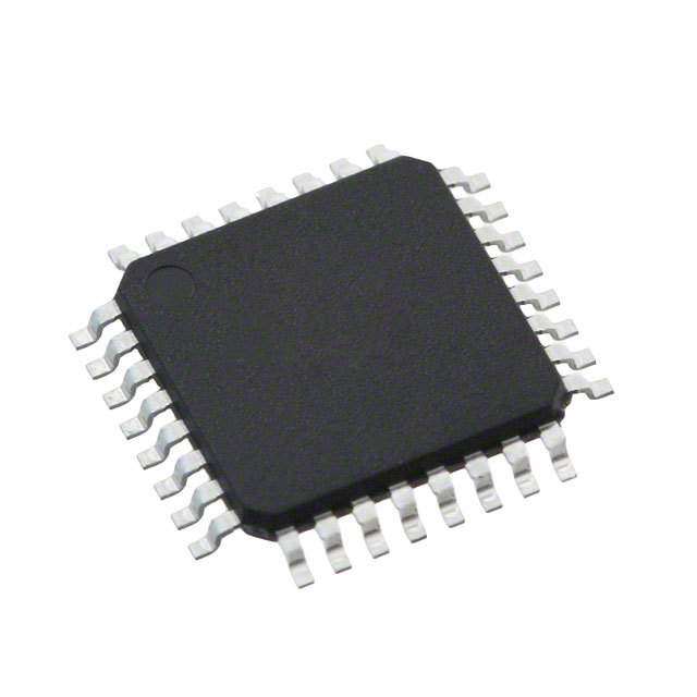
Microchip Technology 的 ATMEGA169P-16MU 是一款基于 AVR RISC 架构的 8 位高性能微控制器,广泛应用于多种嵌入式控制系统中。其主要应用场景包括:

1. 消费类电子产品:如智能家电、遥控器、电子玩具等,ATMEGA169P-16MU 凭借其低功耗和高集成度,适合用于各类便携式设备的控制核心。

2. 工业控制:可用于工业自动化设备中的传感器控制、电机控制、人机界面(如 LCD 显示控制)等,具备较强的抗干扰能力和稳定性。

3. 汽车电子:适用于车身控制系统、仪表盘显示、车载传感器等对可靠性要求较高的环境。

4. 智能仪表:如电表、水表、气表等智能计量设备,利用其内部的 ADC、定时器等功能实现精确测量与数据处理。

5. 教育与开发平台:由于其开发资源丰富,常用于嵌入式教学、学生实验及原型开发。

该芯片工作温度范围宽(-40℃ 至 +85℃),采用 44-TQFP 封装,适合各种中低端嵌入式应用场景。
| 参数 | 数值 |
| 产品目录 | 集成电路 (IC) |
| 描述 | IC MCU 8BIT 16KB FLASH 64QFN |
| EEPROM容量 | 512 x 8 |
| 产品分类 | |
| I/O数 | 54 |
| 品牌 | Atmel |
| 数据手册 | |
| 产品图片 |
|
| 产品型号 | ATMEGA169P-16MU |
| PCN其它 | |
| RAM容量 | 1K x 8 |
| rohs | 无铅 / 符合限制有害物质指令(RoHS)规范要求 |
| 产品系列 | AVR® ATmega |
| 产品培训模块 | http://www.digikey.cn/PTM/IndividualPTM.page?site=cn&lang=zhs&ptm=23369http://www.digikey.cn/PTM/IndividualPTM.page?site=cn&lang=zhs&ptm=24997http://www.digikey.cn/PTM/IndividualPTM.page?site=cn&lang=zhs&ptm=25692http://www.digikey.cn/PTM/IndividualPTM.page?site=cn&lang=zhs&ptm=26162http://www.digikey.cn/PTM/IndividualPTM.page?site=cn&lang=zhs&ptm=26159http://www.digikey.cn/PTM/IndividualPTM.page?site=cn&lang=zhs&ptm=26180 |
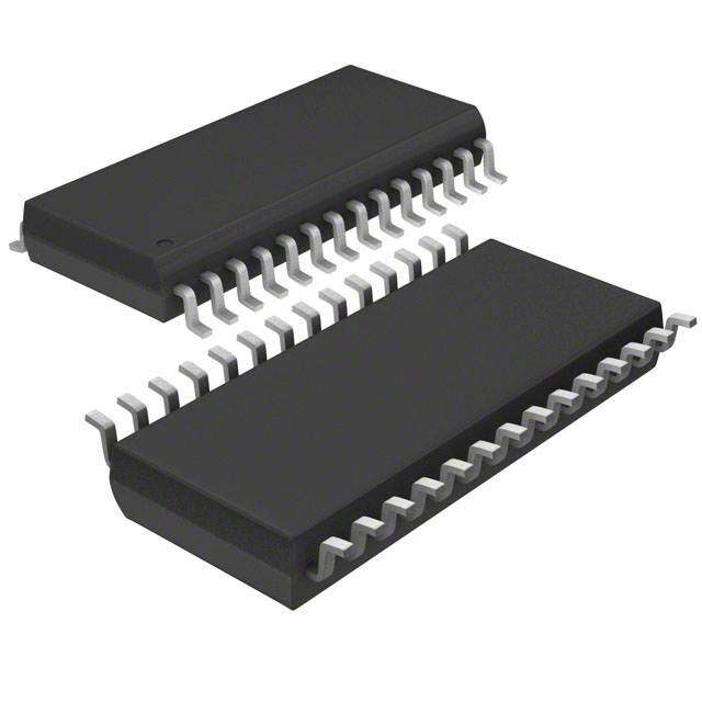
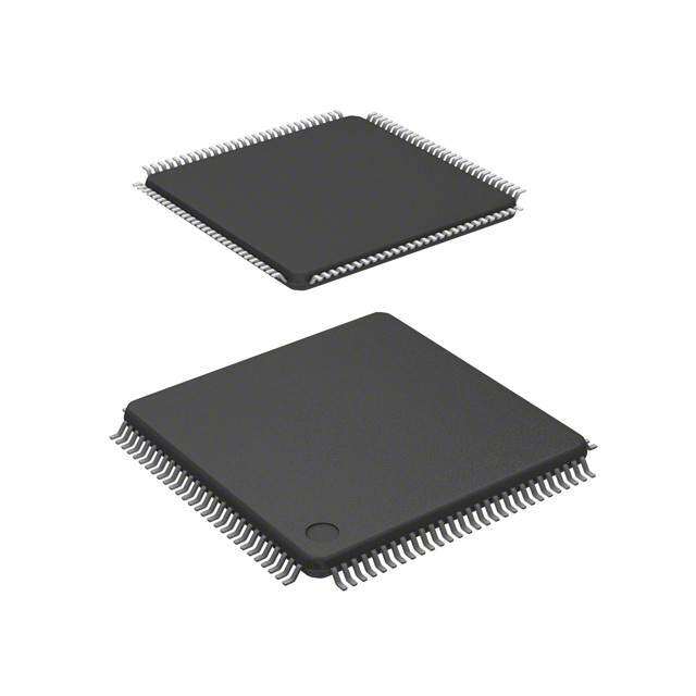
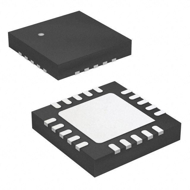
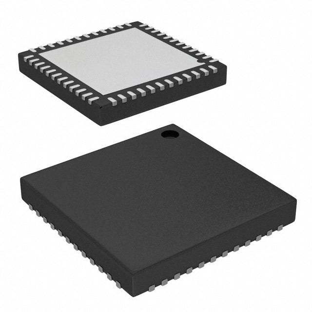
| 供应商器件封装 | 64-QFN(9x9) |
| 其它名称 | ATMEGA169P16MU |
| 包装 | 托盘 |
| 外设 | 欠压检测/复位,LCD,POR,PWM,WDT |
| 封装/外壳 | 64-VFQFN 裸露焊盘 |
| 工作温度 | -40°C ~ 85°C |
| 振荡器类型 | 内部 |
| 数据转换器 | A/D 8x10b |
| 标准包装 | 260 |
| 核心处理器 | AVR |
| 核心尺寸 | 8-位 |
| 电压-电源(Vcc/Vdd) | 2.7 V ~ 5.5 V |
| 程序存储器类型 | 闪存 |
| 程序存储容量 | 16KB(8K x 16) |
| 连接性 | SPI,UART/USART,USI |
| 速度 | 16MHz |
| 配用 | /product-detail/zh/ATSTK600-TQFP64/ATSTK600-TQFP64-ND/1886238/product-detail/zh/ATAVRISP2/ATAVRISP2-ND/898891/product-detail/zh/ATJTAGICE2/ATJTAGICE2-ND/639537/product-detail/zh/ATAVRBFLY/ATAVRBFLY-ND/562203/product-detail/zh/ATSTK502/ATSTK502-ND/522037/product-detail/zh/ATSTK500/ATSTK500-ND/355495 |


- 商务部:美国ITC正式对集成电路等产品启动337调查
- 曝三星4nm工艺存在良率问题 高通将骁龙8 Gen1或转产台积电
- 太阳诱电将投资9.5亿元在常州建新厂生产MLCC 预计2023年完工
- 英特尔发布欧洲新工厂建设计划 深化IDM 2.0 战略
- 台积电先进制程称霸业界 有大客户加持明年业绩稳了
- 达到5530亿美元!SIA预计今年全球半导体销售额将创下新高
- 英特尔拟将自动驾驶子公司Mobileye上市 估值或超500亿美元
- 三星加码芯片和SET,合并消费电子和移动部门,撤换高东真等 CEO
- 三星电子宣布重大人事变动 还合并消费电子和移动部门
- 海关总署:前11个月进口集成电路产品价值2.52万亿元 增长14.8%


PDF Datasheet 数据手册内容提取
Features • High Performance, Low Power Atmel® AVR® 8-Bit Microcontroller (cid:129) Advanced RISC Architecture – 130 Powerful Instructions – Most Single Clock Cycle Execution – 32 × 8 General Purpose Working Registers – Fully Static Operation – Up to 16 MIPS Throughput at 16 MHz – On-Chip 2-cycle Multiplier (cid:129) High Endurance Non-volatile Memory segments – 16 Kbytes of In-System Self-programmable Flash program memory – 512 Bytes EEPROM 8-bit – 1 Kbytes Internal SRAM – Write/Erase cycles: 10,000 Flash/100,000 EEPROM – Data retention: 20 years at 85°C/100 years at 25°C(1) Microcontroller – Optional Boot Code Section with Independent Lock Bits In-System Programming by On-chip Boot Program with 16K Bytes True Read-While-Write Operation – Programming Lock for Software Security (cid:129) JTAG (IEEE std. 1149.1 compliant) Interface In-System – Boundary-scan Capabilities According to the JTAG Standard – Extensive On-chip Debug Support Programmable – Programming of Flash, EEPROM, Fuses, and Lock Bits through the JTAG Interface (cid:129) Peripheral Features Flash – 4 × 25 Segment LCD Driver – Two 8-bit Timer/Counters with Separate Prescaler and Compare Mode – One 16-bit Timer/Counter with Separate Prescaler, Compare Mode, and Capture Mode – Real Time Counter with Separate Oscillator ATmega169P – Four PWM Channels – 8-channel, 10-bit ADC ATmega169PV – Programmable Serial USART – Master/Slave SPI Serial Interface – Universal Serial Interface with Start Condition Detector – Programmable Watchdog Timer with Separate On-chip Oscillator – On-chip Analog Comparator Preliminary – Interrupt and Wake-up on Pin Change (cid:129) Special Microcontroller Features – Power-on Reset and Programmable Brown-out Detection – Internal Calibrated Oscillator – External and Internal Interrupt Sources Summary – Five Sleep Modes: Idle, ADC Noise Reduction, Power-save, Power-down, and Standby (cid:129) I/O and Packages – 54 Programmable I/O Lines – 64-lead TQFP, 64-pad QFN/MLF and 64-pad DRQFN (cid:129) Speed Grade: – ATmega169PV: 0 - 4 MHz @ 1.8V - 5.5V, 0 - 8 MHz @ 2.7V - 5.5V – ATmega169P: 0 - 8 MHz @ 2.7V - 5.5V, 0 - 16 MHz @ 4.5V - 5.5V (cid:129) Temperature range: – -40°C to 85°C Industrial (cid:129) Ultra-Low Power Consumption – Active Mode: 1 MHz, 1.8V: 330 µA 32 kHz, 1.8V: 10 µA (including Oscillator) 32 kHz, 1.8V: 25 µA (including Oscillator and LCD) – Power-down Mode: 0.1 µA at 1.8V – Power-save Mode: 0.6 µA at 1.8V (Including 32 kHz RTC) Rev. 8018PS–AVR–08/10
ATmega169P 1. Pin Configurations 1.1 Pinout - TQFP/QFN/MLF Figure 1-1. 64A (TQFP)and 64M1 (QFN/MLF) Pinout ATmega169P CK) MS) DO) DI) C0) C1) C2) C3) C4/T C5/T C6/T C7/T M0) M1) M2) D D D D D D D D O O O VCC ND REF F0 (A F1 (A F2 (A F3 (A F4 (A F5 (A F6 (A F7 (A ND CC A0 (C A1 (C A2 (C A G A P P P P P P P P G V P P P 4 3 2 1 0 9 8 7 6 5 4 3 2 1 0 9 6 6 6 6 6 5 5 5 5 5 5 5 5 5 5 4 LCDCAP 1 48 PA3 (COM3) (RXD/PCINT0) PE0 2 47 PA4 (SEG0) INDEX CORNER (TXD/PCINT1) PE1 3 46 PA5 (SEG1) (XCK/AIN0/PCINT2) PE2 4 45 PA6 (SEG2) (AIN1/PCINT3) PE3 5 44 PA7 (SEG3) (USCK/SCL/PCINT4) PE4 6 43 PG2 (SEG4) (DI/SDA/PCINT5) PE5 7 42 PC7 (SEG5) (DO/PCINT6) PE6 8 41 PC6 (SEG6) (CLKO/PCINT7) PE7 9 40 PC5 (SEG7) (SS/PCINT8) PB0 10 39 PC4 (SEG8) (SCK/PCINT9) PB1 11 38 PC3 (SEG9) (MOSI/PCINT10) PB2 12 37 PC2 (SEG10) (MISO/PCINT11) PB3 13 36 PC1 (SEG11) (OC0A/PCINT12) PB4 14 35 PC0 (SEG12) (OC1A/PCINT13) PB5 15 34 PG1 (SEG13) (OC1B/PCINT14) PB6 16 33 PG0 (SEG14) 7 8 9 0 1 2 3 4 5 6 7 8 9 0 1 2 1 1 1 2 2 2 2 2 2 2 2 2 2 3 3 3 7 3 4 5 C D 2 1 0 1 2 3 4 5 6 7 B G G G C N L L D D D D D D D D T15) P G24) P G23) P SET/P V G 2) XTA 1) XTA G22) P G21) P G20) P G19) P G18) P G17) P G16) P G15) P N E E E C C E E E E E E E E CI S S R S S S S S S S S S S 2A/P (T1/ (T0/ (TO (TO CP1/ NT0/ ( ( ( ( ( ( OC (I (I ( Note: The large center pad underneath the QFN/MLF packages is made of metal and internally connected to GND. It should be sol- dered or glued to the board to ensure good mechanical stability. If the center pad is left unconnected, the package might loosen from the board. 2 8018PS–AVR–08/10
ATmega169P 1.2 Pinout - DRQFN Figure 1-2. 64MC (DRQFN) Pinout ATmega169P Top view Bottom view A34B30 A33B29 A32B28 A31B27 A30B26 A29B25 A28B24 A27B23 A26 A26B23 A27B24 A28B25 A29B26 A30B27 A31B28 A32B29 A33B30 A34 A1 A25 A25 A1 B1 B22 B22 B1 A2 A24 A24 A2 B2 B21 B21 B2 A3 A23 A23 A3 B3 B20 B20 B3 A4 A22 A22 A4 B4 B19 B19 B4 A5 A21 A21 A5 B5 B18 B18 B5 A6 A20 A20 A6 B6 B17 B17 B6 A7 A19 A19 A7 B7 B16 B16 B7 A8 A18 A18 A8 A9 B8A10 B9A11 B10A12 B11A13 B12A14 B13A15 B14A16 B15A17 A17 B15A16 B14A15 B13A14 B12A13 B11A12 B10A11 B9A10 B8A9 Table 1-1. DRQFN-64 Pinout ATmega169P. A1 PE0 A9 PB7 A18 PG1 (SEG13) A26 PA2 (COM2) B1 VLCDCAP B8 PB6 B16 PG0 (SEG14) B23 PA3 (COM3) A2 PE1 A10 PG3 A19 PC0 (SEG12) A27 PA1 (COM1) B2 PE2 B9 PG4 B17 PC1 (SEG11) B24 PA0 (COM0) A3 PE3 A11 RESET A20 PC2 (SEG10) A28 VCC B3 PE4 B10 VCC B18 PC3 (SEG9) B25 GND A4 PE5 A12 GND A21 PC4 (SEG8) A29 PF7 B4 PE6 B11 XTAL2 (TOSC2) B19 PC5 (SEG7) B26 PF6 A5 PE7 A13 XTAL1 (TOSC1) A22 PC6 (SEG6) A30 PF5 B5 PB0 B12 PD0 (SEG22) B20 PC7 (SEG5) B27 PF4 A6 PB1 A14 PD1 (SEG21) A23 PG2 (SEG4) A31 PF3 B6 PB2 B13 PD2 (SEG20) B21 PA7 (SEG3) B28 PF2 A7 PB3 A15 PD3 (SEG19) A24 PA6 (SEG2) A32 PF1 B7 PB5 B14 PD4 (SEG18) B22 PA4 (SEG0) B29 PF0 A8 PB4 A16 PD5 (SEG17) A25 PA5 (SEG1) A33 AREF B15 PD7 (SEG15) B30 AVCC A17 PD6 (SEG16) A34 GND 3 8018PS–AVR–08/10
ATmega169P 2. Overview The ATmega169P is a low-power CMOS 8-bit microcontroller based on the AVR enhanced RISC architecture. By execut- ing powerful instructions in a single clock cycle, the ATmega169P achieves throughputs approaching 1 MIPS per MHz allowing the system designer to optimize power consumption versus processing speed. 2.1 Block Diagram Figure 2-1. Block Diagram 1 2 PF0 - PF7 PA0 - PA7 PC0 - PC7 AL AL T T X X VCC GND PORTF DRIVERS PORTA DRIVERS PORTC DRIVERS DATAREGISTER DATADIR. DATAREGISTER DATADIR. DATAREGISTER DATADIR. PORTF REG.PORTF PORTA REG.PORTA PORTC REG.PORTC 8-BIT DATA BUS AVCC CALIB. OSC ADC INTERNAL OSCILLATOR AREF OSCILLATOR PROGRAM STACK WATCHDOG JTAG TAP COUNTER POINTER TIMER TIMING AND CONTROL LCD ON-CHIP DEBUG PRFOLAGSRHAM SRAM MCRUE GCOISNTTERROL CONDTRRIVOELRLER/ BOUSNCDAANRY- INRSETGRUISCTTEIRON PGUERNPEORSAEL COTUIMNETRER/S REGISTERS X PROGLORAGMICMING INDSETRCUOCDTEIRON YZ INTEURNRITUPT T COLNINTERSOL ALU EEPROM RESE STATUS AVR CPU REGISTER USART UNIVERSAL SPI SERIAL INTERFACE R O ANALOGMPARAT +- DATAPROERGTIESTER RDEAGT.APODRIRT.E DATAPROERGTIBSTER RDEAGT.APODRIRT.B DATAPROERGTDISTER RDEAGT.APODRIRT.D DAPTOARRTEGG. RDEAGTA.PDOIRR.TG O C PORTE DRIVERS PORTB DRIVERS PORTD DRIVERS PORTG DRIVERS PE0 - PE7 PB0 - PB7 PD0 - PD7 PG0 - PG4 4 8018PS–AVR–08/10
ATmega169P The AVR core combines a rich instruction set with 32 general purpose working registers. All the 32 registers are directly connected to the Arithmetic Logic Unit (ALU), allowing two independent registers to be accessed in one single instruction executed in one clock cycle. The resulting architecture is more code efficient while achieving throughputs up to ten times faster than con- ventional CISC microcontrollers. The ATmega169P provides the following features: 16 Kbytes of In-System Programmable Flash with Read-While-Write capabilities, 512 bytes EEPROM, 1 Kbyte SRAM, 53general purpose I/O lines, 32 general purpose working registers, a JTAG interface for Boundary-scan, On-chip Debugging support and programming, a complete On-chip LCD controller with internal step-up voltage, three flexible Timer/Counters with compare modes, internal and external interrupts, a serial programmable USART, Universal Serial Interface with Start Condition Detector, an 8- channel, 10-bit ADC, a programmable Watchdog Timer with internal Oscillator, an SPI serial port, and five software selectable power saving modes. The Idle mode stops the CPU while allowing the SRAM, Timer/Counters, SPI port, and interrupt system to continue functioning. The Power-down mode saves the register contents but freezes the Oscillator, disabling all other chip functions until the next interrupt or hardware reset. In Power-save mode, the asynchronous timer and the LCD controller continues to run, allowing the user to maintain a timer base and operate the LCD display while the rest of the device is sleeping. The ADC Noise Reduction mode stops the CPU and all I/O modules except asynchronous timer, LCD controller and ADC, to minimize switching noise during ADC conversions. In Standby mode, the crystal/resonator Oscillator is running while the rest of the device is sleeping. This allows very fast start-up com- bined with low-power consumption. The device is manufactured using Atmel’s high density non-volatile memory technology. The On-chip ISP Flash allows the program memory to be reprogrammed In-System through an SPI serial interface, by a conventional non-volatile memory programmer, or by an On-chip Boot pro- gram running on the AVR core. The Boot program can use any interface to download the application program in the Application Flash memory. Software in the Boot Flash section will continue to run while the Application Flash section is updated, providing true Read-While-Write operation. By combining an 8-bit RISC CPU with In-System Self-Programmable Flash on a monolithic chip, the Atmel ATmega169P is a powerful microcontroller that provides a highly flex- ible and cost effective solution to many embedded control applications. The ATmega169P AVR is supported with a full suite of program and system development tools including: C Compilers, Macro Assemblers, Program Debugger/Simulators, In-Circuit Emulators, and Evaluation kits. 5 8018PS–AVR–08/10
ATmega169P 2.2 Pin Descriptions 2.2.1 VCC Digital supply voltage. 2.2.2 GND Ground. 2.2.3 Port A (PA7:PA0) Port A is an 8-bit bi-directional I/O port with internal pull-up resistors (selected for each bit). The Port A output buffers have symmetrical drive characteristics with both high sink and source capability. As inputs, Port A pins that are externally pulled low will source current if the pull-up resistors are activated. The Port A pins are tri-stated when a reset condition becomes active, even if the clock is not running. Port A also serves the functions of various special features of the ATmega169P as listed on ”Alternate Functions of Port A” on page 73. 2.2.4 Port B (PB7:PB0) Port B is an 8-bit bi-directional I/O port with internal pull-up resistors (selected for each bit). The Port B output buffers have symmetrical drive characteristics with both high sink and source capability. As inputs, Port B pins that are externally pulled low will source current if the pull-up resistors are activated. The Port B pins are tri-stated when a reset condition becomes active, even if the clock is not running. Port B has better driving capabilities than the other ports. Port B also serves the functions of various special features of the ATmega169P as listed on ”Alternate Functions of Port B” on page 74. 2.2.5 Port C (PC7:PC0) Port C is an 8-bit bi-directional I/O port with internal pull-up resistors (selected for each bit). The Port C output buffers have symmetrical drive characteristics with both high sink and source capability. As inputs, Port C pins that are externally pulled low will source current if the pull-up resistors are activated. The Port C pins are tri-stated when a reset condition becomes active, even if the clock is not running. Port C also serves the functions of special features of the ATmega169P as listed on ”Alternate Functions of Port C” on page 77. 2.2.6 Port D (PD7:PD0) Port D is an 8-bit bi-directional I/O port with internal pull-up resistors (selected for each bit). The Port D output buffers have symmetrical drive characteristics with both high sink and source capability. As inputs, Port D pins that are externally pulled low will source current if the pull-up resistors are activated. The Port D pins are tri-stated when a reset condition becomes active, even if the clock is not running. Port D also serves the functions of various special features of the ATmega169P as listed on ”Alternate Functions of Port D” on page 79. 6 8018PS–AVR–08/10
ATmega169P 2.2.7 Port E (PE7:PE0) Port E is an 8-bit bi-directional I/O port with internal pull-up resistors (selected for each bit). The Port E output buffers have symmetrical drive characteristics with both high sink and source capability. As inputs, Port E pins that are externally pulled low will source current if the pull-up resistors are activated. The Port E pins are tri-stated when a reset condition becomes active, even if the clock is not running. Port E also serves the functions of various special features of the ATmega169P as listed on ”Alternate Functions of Port E” on page 81. 2.2.8 Port F (PF7:PF0) Port F serves as the analog inputs to the A/D Converter. Port F also serves as an 8-bit bi-directional I/O port, if the A/D Converter is not used. Port pins can provide internal pull-up resistors (selected for each bit). The Port F output buffers have sym- metrical drive characteristics with both high sink and source capability. As inputs, Port F pins that are externally pulled low will source current if the pull-up resistors are activated. The Port F pins are tri-stated when a reset condition becomes active, even if the clock is not running. If the JTAG interface is enabled, the pull-up resistors on pins PF7(TDI), PF5(TMS), and PF4(TCK) will be activated even if a reset occurs. Port F also serves the functions of the JTAG interface, see ”Alternate Functions of Port F” on page 83. 2.2.9 Port G (PG5:PG0) Port G is a 6-bit bi-directional I/O port with internal pull-up resistors (selected for each bit). The Port G output buffers have symmetrical drive characteristics with both high sink and source capability. As inputs, Port G pins that are externally pulled low will source current if the pull-up resistors are activated. The Port G pins are tri-stated when a reset condition becomes active, even if the clock is not running. Port G also serves the functions of various special features of the ATmega169P as listed on page 85. 2.2.10 RESET Reset input. A low level on this pin for longer than the minimum pulse length will generate a reset, even if the clock is not running. The minimum pulse length is given in Table 28-4 on page 333. Shorter pulses are not guaranteed to generate a reset. 2.2.11 XTAL1 Input to the inverting Oscillator amplifier and input to the internal clock operating circuit. 2.2.12 XTAL2 Output from the inverting Oscillator amplifier. 2.2.13 AVCC AVCC is the supply voltage pin for Port F and the A/D Converter. It should be externally con- nected to V , even if the ADC is not used. If the ADC is used, it should be connected to V CC CC through a low-pass filter. 7 8018PS–AVR–08/10
ATmega169P 2.2.14 AREF This is the analog reference pin for the A/D Converter. 2.2.15 LCDCAP An external capacitor (typical > 470 nF) must be connected to the LCDCAP pin as shown in Fig- ure 23-2 on page 236. This capacitor acts as a reservoir for LCD power (V ). A large LCD capacitance reduces ripple on V but increases the time until V reaches its target value. LCD LCD 8 8018PS–AVR–08/10
ATmega169P 3. Resources A comprehensive set of development tools, application notes and datasheets are available for download on http://www.atmel.com/avr. Note: 1. 4. Data Retention Reliability Qualification results show that the projected data retention failure rate is much less than 1 PPM over 20 years at 85°C or 100 years at 25°C. 9 8018PS–AVR–08/10
ATmega169P 5. Register Summary Address Name Bit 7 Bit 6 Bit 5 Bit 4 Bit 3 Bit 2 Bit 1 Bit 0 Page (0xFF) Reserved – – – – – – – – (0xFE) LCDDR18 – – – – – – – SEG324 250 (0xFD) LCDDR17 SEG323 SEG322 SEG321 SEG320 SEG319 SEG318 SEG317 SEG316 250 (0xFC) LCDDR16 SEG315 SEG314 SEG313 SEG312 SEG311 SEG310 SEG309 SEG308 250 (0xFB) LCDDR15 SEG307 SEG306 SEG305 SEG304 SEG303 SEG302 SEG301 SEG300 250 (0xFA) Reserved – – – – – – – – (0xF9) LCDDR13 – – – – – – – SEG224 250 (0xF8) LCDDR12 SEG223 SEG222 SEG221 SEG220 SEG219 SEG218 SEG217 SEG216 250 (0xF7) LCDDR11 SEG215 SEG214 SEG213 SEG212 SEG211 SEG210 SEG209 SEG208 250 (0xF6) LCDDR10 SEG207 SEG206 SEG205 SEG204 SEG203 SEG202 SEG201 SEG200 250 (0xF5) Reserved – – – – – – – – (0xF4) LCDDR8 – – – – – – – SEG124 250 (0xF3) LCDDR7 SEG123 SEG122 SEG121 SEG120 SEG119 SEG118 SEG117 SEG116 250 (0xF2) LCDDR6 SEG115 SEG114 SEG113 SEG112 SEG111 SEG110 SEG109 SEG108 250 (0xF1) LCDDR5 SEG107 SEG106 SEG105 SEG104 SEG103 SEG102 SEG101 SEG100 250 (0xF0) Reserved – – – – – – – – (0xEF) LCDDR3 – – – – – – – SEG024 250 (0xEE) LCDDR2 SEG023 SEG022 SEG021 SEG020 SEG019 SEG018 SEG017 SEG016 250 (0xED) LCDDR1 SEG015 SEG014 SEG013 SEG012 SEG011 SEG010 SEG09 SEG008 250 (0xEC) LCDDR0 SEG007 SEG006 SEG005 SEG004 SEG003 SEG002 SEG001 SEG000 250 (0xEB) Reserved – – – – – – – – (0xEA) Reserved – – – – – – – – (0xE9) Reserved – – – – – – – – (0xE8) Reserved – – – – – – – – (0xE7) LCDCCR LCDDC2 LCDDC1 LCDDC0 LCDMDT LCDCC3 LCDCC2 LCDCC1 LCDCC0 249 (0xE6) LCDFRR – LCDPS2 LCDPS1 LCDPS0 – LCDCD2 LCDCD1 LCDCD0 247 (0xE5) LCDCRB LCDCS LCD2B LCDMUX1 LCDMUX0 – LCDPM2 LCDPM1 LCDPM0 246 (0xE4) LCDCRA LCDEN LCDAB – LCDIF LCDIE LCDBD LCDCCD LCDBL 245 (0xE3) Reserved – – – – – – – – (0xE2) Reserved – – – – – – – – (0xE1) Reserved – – – – – – – – (0xE0) Reserved – – – – – – – – (0xDF) Reserved – – – – – – – – (0xDE) Reserved – – – – – – – – (0xDD) Reserved – – – – – – – – (0xDC) Reserved – – – – – – – – (0xDB) Reserved – – – – – – – – (0xDA) Reserved – – – – – – – – (0xD9) Reserved – – – – – – – – (0xD8) Reserved – – – – – – – – (0xD7) Reserved – – – – – – – – (0xD6) Reserved – – – – – – – – (0xD5) Reserved – – – – – – – – (0xD4) Reserved – – – – – – – – (0xD3) Reserved – – – – – – – – (0xD2) Reserved – – – – – – – – (0xD1) Reserved – – – – – – – – (0xD0) Reserved – – – – – – – – (0xCF) Reserved – – – – – – – – (0xCE) Reserved – – – – – – – – (0xCD) Reserved – – – – – – – – (0xCC) Reserved – – – – – – – – (0xCB) Reserved – – – – – – – – (0xCA) Reserved – – – – – – – – (0xC9) Reserved – – – – – – – – (0xC8) Reserved – – – – – – – – (0xC7) Reserved – – – – – – – – (0xC6) UDR0 USART0 I/O Data Register 190 (0xC5) UBRRH0 USART0 Baud Rate Register High 194 (0xC4) UBRRL0 USART0 Baud Rate Register Low 194 (0xC3) Reserved – – – – – – – – (0xC2) UCSR0C – UMSEL0 UPM01 UPM00 USBS0 UCSZ01 UCSZ00 UCPOL0 190 (0xC1) UCSR0B RXCIE0 TXCIE0 UDRIE0 RXEN0 TXEN0 UCSZ02 RXB80 TXB80 190 (0xC0) UCSR0A RXC0 TXC0 UDRE0 FE0 DOR0 UPE0 U2X0 MPCM0 190 10 8018PS–AVR–08/10
ATmega169P Address Name Bit 7 Bit 6 Bit 5 Bit 4 Bit 3 Bit 2 Bit 1 Bit 0 Page (0xBF) Reserved – – – – – – – – (0xBE) Reserved – – – – – – – – (0xBD) Reserved – – – – – – – – (0xBC) Reserved – – – – – – – – (0xBB) Reserved – – – – – – – – (0xBA) USIDR USI Data Register 207 (0xB9) USISR USISIF USIOIF USIPF USIDC USICNT3 USICNT2 USICNT1 USICNT0 207 (0xB8) USICR USISIE USIOIE USIWM1 USIWM0 USICS1 USICS0 USICLK USITC 208 (0xB7) Reserved – – – – – – – (0xB6) ASSR – – – EXCLK AS2 TCN2UB OCR2UB TCR2UB 156 (0xB5) Reserved – – – – – – – – (0xB4) Reserved – – – – – – – – (0xB3) OCR2A Timer/Counter2 Output Compare Register A 155 (0xB2) TCNT2 Timer/Counter2 (8-bit) 155 (0xB1) Reserved – – – – – – – – (0xB0) TCCR2A FOC2A WGM20 COM2A1 COM2A0 WGM21 CS22 CS21 CS20 153 (0xAF) Reserved – – – – – – – – (0xAE) Reserved – – – – – – – – (0xAD) Reserved – – – – – – – – (0xAC) Reserved – – – – – – – – (0xAB) Reserved – – – – – – – – (0xAA) Reserved – – – – – – – – (0xA9) Reserved – – – – – – – – (0xA8) Reserved – – – – – – – – (0xA7) Reserved – – – – – – – – (0xA6) Reserved – – – – – – – – (0xA5) Reserved – – – – – – – – (0xA4) Reserved – – – – – – – – (0xA3) Reserved – – – – – – – – (0xA2) Reserved – – – – – – – – (0xA1) Reserved – – – – – – – – (0xA0) Reserved – – – – – – – – (0x9F) Reserved – – – – – – – – (0x9E) Reserved – – – – – – – – (0x9D) Reserved – – – – – – – – (0x9C) Reserved – – – – – – – – (0x9B) Reserved – – – – – – – – (0x9A) Reserved – – – – – – – – (0x99) Reserved – – – – – – – – (0x98) Reserved – – – – – – – – (0x97) Reserved – – – – – – – – (0x96) Reserved – – – – – – – – (0x95) Reserved – – – – – – – – (0x94) Reserved – – – – – – – – (0x93) Reserved – – – – – – – – (0x92) Reserved – – – – – – – – (0x91) Reserved – – – – – – – – (0x90) Reserved – – – – – – – – (0x8F) Reserved – – – – – – – – (0x8E) Reserved – – – – – – – – (0x8D) Reserved – – – – – – – – (0x8C) Reserved – – – – – – – – (0x8B) OCR1BH Timer/Counter1 - Output Compare Register B High Byte 132 (0x8A) OCR1BL Timer/Counter1 - Output Compare Register B Low Byte 132 (0x89) OCR1AH Timer/Counter1 - Output Compare Register A High Byte 132 (0x88) OCR1AL Timer/Counter1 - Output Compare Register A Low Byte 132 (0x87) ICR1H Timer/Counter1 - Input Capture Register High Byte 133 (0x86) ICR1L Timer/Counter1 - Input Capture Register Low Byte 133 (0x85) TCNT1H Timer/Counter1 - Counter Register High Byte 132 (0x84) TCNT1L Timer/Counter1 - Counter Register Low Byte 132 (0x83) Reserved – – – – – – – – (0x82) TCCR1C FOC1A FOC1B – – – – – – 131 (0x81) TCCR1B ICNC1 ICES1 – WGM13 WGM12 CS12 CS11 CS10 130 (0x80) TCCR1A COM1A1 COM1A0 COM1B1 COM1B0 – – WGM11 WGM10 128 (0x7F) DIDR1 – – – – – – AIN1D AIN0D 214 (0x7E) DIDR0 ADC7D ADC6D ADC5D ADC4D ADC3D ADC2D ADC1D ADC0D 232 11 8018PS–AVR–08/10
ATmega169P Address Name Bit 7 Bit 6 Bit 5 Bit 4 Bit 3 Bit 2 Bit 1 Bit 0 Page (0x7D) Reserved – – – – – – – – (0x7C) ADMUX REFS1 REFS0 ADLAR MUX4 MUX3 MUX2 MUX1 MUX0 228 (0x7B) ADCSRB – ACME – – – ADTS2 ADTS1 ADTS0 213, 232 (0x7A) ADCSRA ADEN ADSC ADATE ADIF ADIE ADPS2 ADPS1 ADPS0 230 (0x79) ADCH ADC Data Register High byte 231 (0x78) ADCL ADC Data Register Low byte 231 (0x77) Reserved – – – – – – – – (0x76) Reserved – – – – – – – – (0x75) Reserved – – – – – – – – (0x74) Reserved – – – – – – – – (0x73) Reserved – – – – – – – – (0x72) Reserved – – – – – – – – (0x71) Reserved – – – – – – – – (0x70) TIMSK2 – – – – – – OCIE2A TOIE2 156 (0x6F) TIMSK1 – – ICIE1 – – OCIE1B OCIE1A TOIE1 133 (0x6E) TIMSK0 – – – – – – OCIE0A TOIE0 104 (0x6D) Reserved – – – – – – – – (0x6C) PCMSK1 PCINT15 PCINT14 PCINT13 PCINT12 PCINT11 PCINT10 PCINT9 PCINT8 63 (0x6B) PCMSK0 PCINT7 PCINT6 PCINT5 PCINT4 PCINT3 PCINT2 PCINT1 PCINT0 64 (0x6A) Reserved – – – – – – – – (0x69) EICRA – – – – – – ISC01 ISC00 62 (0x68) Reserved – – – – – – – – (0x67) Reserved – – – – – – – – (0x66) OSCCAL Oscillator Calibration Register 38 (0x65) Reserved – – – – – – – – (0x64) PRR – – – PRLCD PRTIM1 PRSPI PRUSART0 PRADC 45 (0x63) Reserved – – – – – – – – (0x62) Reserved – – – – – – – – (0x61) CLKPR CLKPCE – – – CLKPS3 CLKPS2 CLKPS1 CLKPS0 38 (0x60) WDTCR – – – WDCE WDE WDP2 WDP1 WDP0 54 0x3F (0x5F) SREG I T H S V N Z C 13 0x3E (0x5E) SPH – – – – – SP10 SP9 SP8 15 0x3D (0x5D) SPL SP7 SP6 SP5 SP4 SP3 SP2 SP1 SP0 15 0x3C (0x5C) Reserved 0x3B (0x5B) Reserved 0x3A (0x5A) Reserved 0x39 (0x59) Reserved 0x38 (0x58) Reserved 0x37 (0x57) SPMCSR SPMIE RWWSB – RWWSRE BLBSET PGWRT PGERS SPMEN 293 0x36 (0x56) Reserved – – – – – – – – 0x35 (0x55) MCUCR JTD – – PUD – – IVSEL IVCE 60, 88, 278 0x34 (0x54) MCUSR – – – JTRF WDRF BORF EXTRF PORF 278 0x33 (0x53) SMCR – – – – SM2 SM1 SM0 SE 45 0x32 (0x52) Reserved – – – – – – – – 0x31 (0x51) OCDR IDRD/OCDR7 OCDR6 OCDR5 OCDR4 OCDR3 OCDR2 OCDR1 OCDR0 257 0x30 (0x50) ACSR ACD ACBG ACO ACI ACIE ACIC ACIS1 ACIS0 213 0x2F (0x4F) Reserved – – – – – – – – 0x2E (0x4E) SPDR SPI Data Register 167 0x2D (0x4D) SPSR SPIF WCOL – – – – – SPI2X 166 0x2C (0x4C) SPCR SPIE SPE DORD MSTR CPOL CPHA SPR1 SPR0 165 0x2B (0x4B) GPIOR2 General Purpose I/O Register 2 29 0x2A (0x4A) GPIOR1 General Purpose I/O Register 1 29 0x29 (0x49) Reserved – – – – – – – – 0x28 (0x48) Reserved – – – – – – – – 0x27 (0x47) OCR0A Timer/Counter0 Output Compare Register A 104 0x26 (0x46) TCNT0 Timer/Counter0 (8 Bit) 104 0x25 (0x45) Reserved – – – – – – – – 0x24 (0x44) TCCR0A FOC0A WGM00 COM0A1 COM0A0 WGM01 CS02 CS01 CS00 102 0x23 (0x43) GTCCR TSM – – – – – PSR2 PSR10 137, 157 0x22 (0x42) EEARH – – – – – – – EEAR8 27 0x21 (0x41) EEARL EEPROM Address Register Low Byte 27 0x20 (0x40) EEDR EEPROM Data Register 27 0x1F (0x3F) EECR – – – – EERIE EEMWE EEWE EERE 27 0x1E (0x3E) GPIOR0 General Purpose I/O Register 0 29 0x1D (0x3D) EIMSK PCIE1 PCIE0 – – – – – INT0 62 0x1C (0x3C) EIFR PCIF1 PCIF0 – – – – – INTF0 63 12 8018PS–AVR–08/10
ATmega169P Address Name Bit 7 Bit 6 Bit 5 Bit 4 Bit 3 Bit 2 Bit 1 Bit 0 Page 0x1B (0x3B) Reserved – – – – – – – – 0x1A (0x3A) Reserved – – – – – – – – 0x19 (0x39) Reserved – – – – – – – – 0x18 (0x38) Reserved – – – – – – – – 0x17 (0x37) TIFR2 – – – – – – OCF2A TOV2 156 0x16 (0x36) TIFR1 – – ICF1 – – OCF1B OCF1A TOV1 134 0x15 (0x35) TIFR0 – – – – – – OCF0A TOV0 105 0x14 (0x34) PORTG – – PORTG5 PORTG4 PORTG3 PORTG2 PORTG1 PORTG0 90 0x13 (0x33) DDRG – – DDG5 DDG4 DDG3 DDG2 DDG1 DDG0 90 0x12 (0x32) PING – – PING5 PING4 PING3 PING2 PING1 PING0 90 0x11 (0x31) PORTF PORTF7 PORTF6 PORTF5 PORTF4 PORTF3 PORTF2 PORTF1 PORTF0 90 0x10 (0x30) DDRF DDF7 DDF6 DDF5 DDF4 DDF3 DDF2 DDF1 DDF0 90 0x0F (0x2F) PINF PINF7 PINF6 PINF5 PINF4 PINF3 PINF2 PINF1 PINF0 90 0x0E (0x2E) PORTE PORTE7 PORTE6 PORTE5 PORTE4 PORTE3 PORTE2 PORTE1 PORTE0 89 0x0D (0x2D) DDRE DDE7 DDE6 DDE5 DDE4 DDE3 DDE2 DDE1 DDE0 89 0x0C (0x2C) PINE PINE7 PINE6 PINE5 PINE4 PINE3 PINE2 PINE1 PINE0 90 0x0B (0x2B) PORTD PORTD7 PORTD6 PORTD5 PORTD4 PORTD3 PORTD2 PORTD1 PORTD0 89 0x0A (0x2A) DDRD DDD7 DDD6 DDD5 DDD4 DDD3 DDD2 DDD1 DDD0 89 0x09 (0x29) PIND PIND7 PIND6 PIND5 PIND4 PIND3 PIND2 PIND1 PIND0 89 0x08 (0x28) PORTC PORTC7 PORTC6 PORTC5 PORTC4 PORTC3 PORTC2 PORTC1 PORTC0 89 0x07 (0x27) DDRC DDC7 DDC6 DDC5 DDC4 DDC3 DDC2 DDC1 DDC0 89 0x06 (0x26) PINC PINC7 PINC6 PINC5 PINC4 PINC3 PINC2 PINC1 PINC0 89 0x05 (0x25) PORTB PORTB7 PORTB6 PORTB5 PORTB4 PORTB3 PORTB2 PORTB1 PORTB0 88 0x04 (0x24) DDRB DDB7 DDB6 DDB5 DDB4 DDB3 DDB2 DDB1 DDB0 88 0x03 (0x23) PINB PINB7 PINB6 PINB5 PINB4 PINB3 PINB2 PINB1 PINB0 88 0x02 (0x22) PORTA PORTA7 PORTA6 PORTA5 PORTA4 PORTA3 PORTA2 PORTA1 PORTA0 88 0x01 (0x21) DDRA DDA7 DDA6 DDA5 DDA4 DDA3 DDA2 DDA1 DDA0 88 0x00 (0x20) PINA PINA7 PINA6 PINA5 PINA4 PINA3 PINA2 PINA1 PINA0 88 Note: 1. For compatibility with future devices, reserved bits should be written to zero if accessed. Reserved I/O memory addresses should never be written. 2. I/O Registers within the address range 0x00 - 0x1F are directly bit-accessible using the SBI and CBI instructions. In these registers, the value of single bits can be checked by using the SBIS and SBIC instructions. 3. Some of the Status Flags are cleared by writing a logical one to them. Note that, unlike most other AVRs, the CBI and SBI instructions will only operate on the specified bit, and can therefore be used on registers containing such Status Flags. The CBI and SBI instructions work with registers 0x00 to 0x1F only. 4. When using the I/O specific commands IN and OUT, the I/O addresses 0x00 - 0x3F must be used. When addressing I/O Registers as data space using LD and ST instructions, 0x20 must be added to these addresses. The ATmega169P is a com- plex microcontroller with more peripheral units than can be supported within the 64 location reserved in Opcode for the IN and OUT instructions. For the Extended I/O space from 0x60 - 0xFF in SRAM, only the ST/STS/STD and LD/LDS/LDD instructions can be used. 13 8018PS–AVR–08/10
ATmega169P 6. Instruction Set Summary Mnemonics Operands Description Operation Flags #Clocks ARITHMETIC AND LOGIC INSTRUCTIONS ADD Rd, Rr Add two Registers Rd ← Rd + Rr Z,C,N,V,H 1 ADC Rd, Rr Add with Carry two Registers Rd ← Rd + Rr + C Z,C,N,V,H 1 ADIW Rdl,K Add Immediate to Word Rdh:Rdl ← Rdh:Rdl + K Z,C,N,V,S 2 SUB Rd, Rr Subtract two Registers Rd ← Rd - Rr Z,C,N,V,H 1 SUBI Rd, K Subtract Constant from Register Rd ← Rd - K Z,C,N,V,H 1 SBC Rd, Rr Subtract with Carry two Registers Rd ← Rd - Rr - C Z,C,N,V,H 1 SBCI Rd, K Subtract with Carry Constant from Reg. Rd ← Rd - K - C Z,C,N,V,H 1 SBIW Rdl,K Subtract Immediate from Word Rdh:Rdl ← Rdh:Rdl - K Z,C,N,V,S 2 AND Rd, Rr Logical AND Registers Rd ← Rd • Rr Z,N,V 1 ANDI Rd, K Logical AND Register and Constant Rd ← Rd • K Z,N,V 1 OR Rd, Rr Logical OR Registers Rd ← Rd v Rr Z,N,V 1 ORI Rd, K Logical OR Register and Constant Rd ← Rd v K Z,N,V 1 EOR Rd, Rr Exclusive OR Registers Rd ← Rd ⊕ Rr Z,N,V 1 COM Rd One’s Complement Rd ← 0xFF − Rd Z,C,N,V 1 NEG Rd Two’s Complement Rd ← 0x00 − Rd Z,C,N,V,H 1 SBR Rd,K Set Bit(s) in Register Rd ← Rd v K Z,N,V 1 CBR Rd,K Clear Bit(s) in Register Rd ← Rd • (0xFF - K) Z,N,V 1 INC Rd Increment Rd ← Rd + 1 Z,N,V 1 DEC Rd Decrement Rd ← Rd − 1 Z,N,V 1 TST Rd Test for Zero or Minus Rd ← Rd • Rd Z,N,V 1 CLR Rd Clear Register Rd ← Rd ⊕ Rd Z,N,V 1 SER Rd Set Register Rd ← 0xFF None 1 MUL Rd, Rr Multiply Unsigned R1:R0 ← Rd x Rr Z,C 2 MULS Rd, Rr Multiply Signed R1:R0 ← Rd x Rr Z,C 2 MULSU Rd, Rr Multiply Signed with Unsigned R1:R0 ← Rd x Rr Z,C 2 FMUL Rd, Rr Fractional Multiply Unsigned R1:R0 ← (Rd x Rr) << 1 Z,C 2 FMULS Rd, Rr Fractional Multiply Signed R1:R0 ← (Rd x Rr) << 1 Z,C 2 FMULSU Rd, Rr Fractional Multiply Signed with Unsigned R1:R0 ← (Rd x Rr) << 1 Z,C 2 BRANCH INSTRUCTIONS RJMP k Relative Jump PC ← PC + k + 1 None 2 IJMP Indirect Jump to (Z) PC ← Z None 2 JMP k Direct Jump PC ← k None 3 RCALL k Relative Subroutine Call PC ← PC + k + 1 None 3 ICALL Indirect Call to (Z) PC ← Z None 3 CALL k Direct Subroutine Call PC ← k None 4 RET Subroutine Return PC ← STACK None 4 RETI Interrupt Return PC ← STACK I 4 CPSE Rd,Rr Compare, Skip if Equal if (Rd = Rr) PC ← PC + 2 or 3 None 1/2/3 CP Rd,Rr Compare Rd − Rr Z, N,V,C,H 1 CPC Rd,Rr Compare with Carry Rd − Rr − C Z, N,V,C,H 1 CPI Rd,K Compare Register with Immediate Rd − K Z, N,V,C,H 1 SBRC Rr, b Skip if Bit in Register Cleared if (Rr(b)=0) PC ← PC + 2 or 3 None 1/2/3 SBRS Rr, b Skip if Bit in Register is Set if (Rr(b)=1) PC ← PC + 2 or 3 None 1/2/3 SBIC P, b Skip if Bit in I/O Register Cleared if (P(b)=0) PC ← PC + 2 or 3 None 1/2/3 SBIS P, b Skip if Bit in I/O Register is Set if (P(b)=1) PC ← PC + 2 or 3 None 1/2/3 BRBS s, k Branch if Status Flag Set if (SREG(s) = 1) then PC←PC+k + 1 None 1/2 BRBC s, k Branch if Status Flag Cleared if (SREG(s) = 0) then PC←PC+k + 1 None 1/2 BREQ k Branch if Equal if (Z = 1) then PC ← PC + k + 1 None 1/2 BRNE k Branch if Not Equal if (Z = 0) then PC ← PC + k + 1 None 1/2 BRCS k Branch if Carry Set if (C = 1) then PC ← PC + k + 1 None 1/2 BRCC k Branch if Carry Cleared if (C = 0) then PC ← PC + k + 1 None 1/2 BRSH k Branch if Same or Higher if (C = 0) then PC ← PC + k + 1 None 1/2 BRLO k Branch if Lower if (C = 1) then PC ← PC + k + 1 None 1/2 BRMI k Branch if Minus if (N = 1) then PC ← PC + k + 1 None 1/2 BRPL k Branch if Plus if (N = 0) then PC ← PC + k + 1 None 1/2 BRGE k Branch if Greater or Equal, Signed if (N ⊕ V= 0) then PC ← PC + k + 1 None 1/2 BRLT k Branch if Less Than Zero, Signed if (N ⊕ V= 1) then PC ← PC + k + 1 None 1/2 BRHS k Branch if Half Carry Flag Set if (H = 1) then PC ← PC + k + 1 None 1/2 BRHC k Branch if Half Carry Flag Cleared if (H = 0) then PC ← PC + k + 1 None 1/2 BRTS k Branch if T Flag Set if (T = 1) then PC ← PC + k + 1 None 1/2 BRTC k Branch if T Flag Cleared if (T = 0) then PC ← PC + k + 1 None 1/2 BRVS k Branch if Overflow Flag is Set if (V = 1) then PC ← PC + k + 1 None 1/2 14 8018PS–AVR–08/10
ATmega169P Mnemonics Operands Description Operation Flags #Clocks BRVC k Branch if Overflow Flag is Cleared if (V = 0) then PC ← PC + k + 1 None 1/2 BRIE k Branch if Interrupt Enabled if ( I = 1) then PC ← PC + k + 1 None 1/2 BRID k Branch if Interrupt Disabled if ( I = 0) then PC ← PC + k + 1 None 1/2 BIT AND BIT-TEST INSTRUCTIONS SBI P,b Set Bit in I/O Register I/O(P,b) ← 1 None 2 CBI P,b Clear Bit in I/O Register I/O(P,b) ← 0 None 2 LSL Rd Logical Shift Left Rd(n+1) ← Rd(n), Rd(0) ← 0 Z,C,N,V 1 LSR Rd Logical Shift Right Rd(n) ← Rd(n+1), Rd(7) ← 0 Z,C,N,V 1 ROL Rd Rotate Left Through Carry Rd(0)←C,Rd(n+1)← Rd(n),C←Rd(7) Z,C,N,V 1 ROR Rd Rotate Right Through Carry Rd(7)←C,Rd(n)← Rd(n+1),C←Rd(0) Z,C,N,V 1 ASR Rd Arithmetic Shift Right Rd(n) ← Rd(n+1), n=0..6 Z,C,N,V 1 SWAP Rd Swap Nibbles Rd(3..0)←Rd(7..4),Rd(7..4)←Rd(3..0) None 1 BSET s Flag Set SREG(s) ← 1 SREG(s) 1 BCLR s Flag Clear SREG(s) ← 0 SREG(s) 1 BST Rr, b Bit Store from Register to T T ← Rr(b) T 1 BLD Rd, b Bit load from T to Register Rd(b) ← T None 1 SEC Set Carry C ← 1 C 1 CLC Clear Carry C ← 0 C 1 SEN Set Negative Flag N ← 1 N 1 CLN Clear Negative Flag N ← 0 N 1 SEZ Set Zero Flag Z ← 1 Z 1 CLZ Clear Zero Flag Z ← 0 Z 1 SEI Global Interrupt Enable I ← 1 I 1 CLI Global Interrupt Disable I ← 0 I 1 SES Set Signed Test Flag S ← 1 S 1 CLS Clear Signed Test Flag S ← 0 S 1 SEV Set Twos Complement Overflow. V ← 1 V 1 CLV Clear Twos Complement Overflow V ← 0 V 1 SET Set T in SREG T ← 1 T 1 CLT Clear T in SREG T ← 0 T 1 SEH Set Half Carry Flag in SREG H ← 1 H 1 CLH Clear Half Carry Flag in SREG H ← 0 H 1 DATA TRANSFER INSTRUCTIONS MOV Rd, Rr Move Between Registers Rd ← Rr None 1 MOVW Rd, Rr Copy Register Word Rd+1:Rd ← Rr+1:Rr None 1 LDI Rd, K Load Immediate Rd ← K None 1 LD Rd, X Load Indirect Rd ← (X) None 2 LD Rd, X+ Load Indirect and Post-Inc. Rd ← (X), X ← X + 1 None 2 LD Rd, - X Load Indirect and Pre-Dec. X ← X - 1, Rd ← (X) None 2 LD Rd, Y Load Indirect Rd ← (Y) None 2 LD Rd, Y+ Load Indirect and Post-Inc. Rd ← (Y), Y ← Y + 1 None 2 LD Rd, - Y Load Indirect and Pre-Dec. Y ← Y - 1, Rd ← (Y) None 2 LDD Rd,Y+q Load Indirect with Displacement Rd ← (Y + q) None 2 LD Rd, Z Load Indirect Rd ← (Z) None 2 LD Rd, Z+ Load Indirect and Post-Inc. Rd ← (Z), Z ← Z+1 None 2 LD Rd, -Z Load Indirect and Pre-Dec. Z ← Z - 1, Rd ← (Z) None 2 LDD Rd, Z+q Load Indirect with Displacement Rd ← (Z + q) None 2 LDS Rd, k Load Direct from SRAM Rd ← (k) None 2 ST X, Rr Store Indirect (X) ← Rr None 2 ST X+, Rr Store Indirect and Post-Inc. (X) ← Rr, X ← X + 1 None 2 ST - X, Rr Store Indirect and Pre-Dec. X ← X - 1, (X) ← Rr None 2 ST Y, Rr Store Indirect (Y) ← Rr None 2 ST Y+, Rr Store Indirect and Post-Inc. (Y) ← Rr, Y ← Y + 1 None 2 ST - Y, Rr Store Indirect and Pre-Dec. Y ← Y - 1, (Y) ← Rr None 2 STD Y+q,Rr Store Indirect with Displacement (Y + q) ← Rr None 2 ST Z, Rr Store Indirect (Z) ← Rr None 2 ST Z+, Rr Store Indirect and Post-Inc. (Z) ← Rr, Z ← Z + 1 None 2 ST -Z, Rr Store Indirect and Pre-Dec. Z ← Z - 1, (Z) ← Rr None 2 STD Z+q,Rr Store Indirect with Displacement (Z + q) ← Rr None 2 STS k, Rr Store Direct to SRAM (k) ← Rr None 2 LPM Load Program Memory R0 ← (Z) None 3 LPM Rd, Z Load Program Memory Rd ← (Z) None 3 LPM Rd, Z+ Load Program Memory and Post-Inc Rd ← (Z), Z ← Z+1 None 3 SPM Store Program Memory (Z) ← R1:R0 None - IN Rd, P In Port Rd ← P None 1 OUT P, Rr Out Port P ← Rr None 1 15 8018PS–AVR–08/10
ATmega169P Mnemonics Operands Description Operation Flags #Clocks PUSH Rr Push Register on Stack STACK ← Rr None 2 POP Rd Pop Register from Stack Rd ← STACK None 2 MCU CONTROL INSTRUCTIONS NOP No Operation None 1 SLEEP Sleep (see specific descr. for Sleep function) None 1 WDR Watchdog Reset (see specific descr. for WDR/timer) None 1 BREAK Break For On-chip Debug Only None N/A 16 8018PS–AVR–08/10
ATmega169P 7. Ordering Information Speed (MHz)(3) Power Supply Ordering Code Package(1)(2) Operation Range ATmega169PV-8AU 64A Industrial 8 1.8V - 5.5V ATmega169PV-8MU 64M1 (-40°C to 85°C) ATmega169PV-8MCH 64MC ATmega169P-16AU 64A Industrial 16 2.7V - 5.5V ATmega169P-16MU 64M1 (-40°C to 85°C) ATmega169P-16MCH 64MC Notes: 1. This device can also be supplied in wafer form. Please contact your local Atmel sales office for detailed ordering information and minimum quantities. 2. Pb-free packaging, complies to the European Directive for Restriction of Hazardous Substances (RoHS directive). Also Halide free and fully Green. 3. For Speed vs. V , see Figure 28-1 on page 331 and Figure 28-2 on page 332. CC Package Type 64A 64-Lead, Thin (1.0 mm) Plastic Gull Wing Quad Flat Package (TQFP) 64M1 64-pad, 9 × 9 × 1.0 mm body, lead pitch 0.50 mm, Quad Flat No-Lead/Micro Lead Frame Package (QFN/MLF) 64MC 64-lead (2-row Staggered), 7 × 7 × 1.0 mm body, 4.0 × 4.0 mm Exposed Pad, Quad Flat No-Lead Package (QFN) 17 8018PS–AVR–08/10
ATmega169P 8. Packaging Information 8.1 64A PIN 1 B PIN 1 IDENTIFIER e E1 E D1 D C 0°~7° A1 A2 A L COMMON DIMENSIONS (Unit of Measure = mm) SYMBOL MIN NOM MAX NOTE A – – 1.20 A1 0.05 – 0.15 A2 0.95 1.00 1.05 D 15.75 16.00 16.25 D1 13.90 14.00 14.10 Note 2 E 15.75 16.00 16.25 Notes: E1 13.90 14.00 14.10 Note 2 1.This package conforms to JEDEC reference MS-026, Variation AEB. 2. Dimensions D1 and E1 do not include mold protrusion. Allowable B 0.30 – 0.45 protrusion is 0.25 mm per side. Dimensions D1 and E1 are maximum C 0.09 – 0.20 plastic body size dimensions including mold mismatch. 3. Lead coplanarity is 0.10 mm maximum. L 0.45 – 0.75 e 0.80 TYP 10/5/2001 TITLE DRAWING NO. REV. 2325 Orchard Parkway 64A, 64-lead, 14 x 14 mm Body Size, 1.0 mm Body Thickness, San Jose, CA 95131 64A B R 0.8 mm Lead Pitch, Thin Profile Plastic Quad Flat Package (TQFP) 18 8018PS–AVR–08/10
ATmega169P 8.2 64M1 D Marked Pin# 1 ID E C SEATING PLANE A1 TOP VIEW A K 0.08 C L Pin #1 Corner SIDE VIEW D2 1 Option A Pin #1 Triangle 2 3 COMMON DIMENSIONS (Unit of Measure = mm) E2 SYMBOL MIN NOM MAX NOTE Option B Pin #1 A 0.80 0.90 1.00 Chamfer (C 0.30) A1 – 0.02 0.05 b 0.18 0.25 0.30 D 8.90 9.00 9.10 D2 5.20 5.40 5.60 K Option C Pin #1 b e Notch E 8.9 0 9.00 9.10 (0.20 R) E2 5.20 5.40 5.60 BOTTOM VIEW e 0.50 BSC L 0.35 0.40 0.45 K 1.25 1.40 1.55 Note: 1. JEDEC Standard MO-220, (SAW Singulation) Fig. 1, VMMD. 2. Dimension and tolerance conform to ASMEY14.5M-1994. 5/25/06 TITLE DRAWING NO. REV. 2325 Orchard Parkway 64M1, 64-pad, 9 x 9 x 1.0 mm Body, Lead Pitch 0.50 mm, R San Jose, CA 95131 5.40 mm Exposed Pad, Micro Lead Frame Package (MLF) 64M1 G 19 8018PS–AVR–08/10
ATmega169P 8.3 64MC C Pin 1 ID D SIDE VIEW y A1 E A TOP VIEW eT/2 eT L A26 A34 R B23 B30 e COMMON DIMENSIONS (Unit of Measure = mm) A25 A1 B22 B1 SYMBOL MIN NOM MAX NOTE R0.20 0.40 b A 0.80 0.90 1.00 A1 0.00 0.02 0.05 D2 b 0.18 0.23 0.28 C 0.20 REF eT D 6.90 7.00 7.10 D2 3.95 4.00 4.05 B16 B7 A18 A8 E 6.90 7.00 7.10 B15 B8 (0.18) REF E2 3.95 4.00 4.05 eT – 0.65 – A17 A9 L E2 K (0.1) REF eR – 0.65 – K 0.20 – – (REF) BOTTOM VIEW L 0.35 0.40 0.45 Note: 1. The terminal #1 ID is a Laser-marked Feature. y 0.00 – 0.075 10/3/07 TITLE GPC DRAWING NO. REV. Package Drawing Contact: 64MC, 64QFN (2-Row Staggered), packagedrawings@atmel.com 7 x 7 x 1.00 mm Body, 4.0 x 4.0 mm Exposed Pad, ZXC 64MC A Quad Flat No Lead Package 20 8018PS–AVR–08/10
ATmega169P 9. Errata 9.1 ATmega169P Rev. G No known errata. 9.2 ATmega169P Rev. A to F Not sampled. 21 8018PS–AVR–08/10
ATmega169P 10. Datasheet Revision History Please note that the referring page numbers in this section are referring to this document. The referring revision in this section are referring to the document revision. 10.1 Rev. 8018P 08/10 1. Status changed to active 2. EEPROM minimum wait delay, Table 27-15 on page 312, has been changed from 9.0 ms to 3.6 ms 3. Datasheet layout and technical terminology updated 10.2 Rev. 8018O 10/09 1. Changed datasheet status to “Mature” 2. Added Capacitance for Low-frequency Crystal Oscillator, Table 8-5 on page 33. 10.3 Rev. 8018N 08/09 1. Updated ”Ordering Information” on page 17, MCU replaced by MCH. 10.4 Rev. 8018M 07/09 1. Updated the last page with new Atmel’s addresses. 10.5 Rev. L 08/08 1. Updated package information in ”Features” on page 1. 2. Added ”Pinout - DRQFN” on page 3: (cid:129) The Staggered QFN is named Dual Row QFN (DRQFN). 10.6 Rev. K 06/08 1. Updated package information in ”Features” on page 1. 2. Removed “Disclaimer” from section ”Pin Configurations” on page 2 3. Added ”64MC (DRQFN) Pinout ATmega169P” on page 3 4. Added ”Data Retention” on page 9. 5. Updated ”Stack Pointer” on page 13. 6. Updated ”Low-frequency Crystal Oscillator” on page 34. 7. Updated ”USART Register Description” on page 194, register descriptions and tables. 8. Updated ”UCSRnB – USART Control and Status Register n B” on page 195. 9. Updated V in ”DC Characteristics” on page 329, by removing 0.2V from the table. IL2 CC 22 8018PS–AVR–08/10
ATmega169P 10. Replaced Figure 29-36 on page 357 by a correct one. 11. Updated ”Ordering Information” on page 17. 12. Added ”64MC” on page 20 package to ”Packaging Information” on page 18. 10.7 Rev. J 08/07 1. Updated ”Features” on page 1. 2. Added ”Minimizing Power Consumption” on page 237 in the LCD section. 3. Updated ”System and Reset Characteristics” on page 333. 10.8 Rev. I 11/06 1. Updated ”Low-frequency Crystal Oscillator” on page 34. 2. Updated Table 8-8 on page 35, Table 8-9 on page 35, Table 8-10 on page 35, Table 28-7 on page 336. 3. Updated note in Table 28-7 on page 336. 10.9 Rev. H 09/06 1. All characterization data moved to ”Electrical Characteristics” on page 329. 2. Updated ”Calibrated Internal RC Oscillator” on page 32. 3. Updated ”System Control and Reset” on page 47. 4. Added note to Table 27-16 on page 314. 5. Updated ”LCD Controller Characteristics” on page 337. 10.10 Rev. G 08/06 1. Updated ”LCD Controller Characteristics” on page 337. 10.11 Rev. F 08/06 1. Updated ”DC Characteristics” on page 329. 2. Updated Table 13-19 on page 84. 10.12 Rev. E 08/06 1. Updated ”Low-frequency Crystal Oscillator” on page 34. 2. Updated ”Device Identification Register” on page 260. 3. Updated ”Signature Bytes” on page 299. 4. Added Table 27-6 on page 299. 23 8018PS–AVR–08/10
ATmega169P 10.13 Rev. D 07/06 1. Updated ”Register Description for I/O-Ports” on page 88. 2. Updated ”Fast PWM Mode” on page 97. 3. Updated ”Fast PWM Mode” on page 120. 4. Updated Table 14-2 on page 102, Table 14-4 on page 103, Table 15-3 on page 129, Table 15-4 on page 130, Table 17-2 on page 153 and Table 17-4 on page 154. 5 Updated ”UCSRnC – USART Control and Status Register n C” on page 196. 6. Updated Features in ”USI – Universal Serial Interface” on page 199. 7. Added ”Clock speed considerations.” on page 206. 8. Updated Features in ”LCD Controller” on page 234. 9. Updated ”Register Summary” on page 10. 10.14 Rev. C 06/06 1. Updated typos. 2. Updated ”Calibrated Internal RC Oscillator” on page 32. 3. Updated ”OSCCAL – Oscillator Calibration Register” on page 38. 4. Added Table 28-2 on page 332. 10.15 Rev. B 04/06 1. Updated ”Calibrated Internal RC Oscillator” on page 32. 10.16 Rev. A 03/06 1. Initial revision. 24 8018PS–AVR–08/10
Headquarters International Atmel Corporation Atmel Asia Atmel Europe Atmel Japan 2325 Orchard Parkway Unit 1-5 & 16, 19/F Le Krebs 9F, Tonetsu Shinkawa Bldg. San Jose, CA 95131 BEA Tower, Millennium City 5 8, Rue Jean-Pierre Timbaud 1-24-8 Shinkawa USA 418 Kwun Tong Road BP 309 Chuo-ku, Tokyo 104-0033 Tel: 1(408) 441-0311 Kwun Tong, Kowloon 78054 Saint-Quentin-en- Japan Fax: 1(408) 487-2600 Hong Kong YvelinesCedex Tel: (81) 3-3523-3551 Tel: (852) 2245-6100 France Fax: (81) 3-3523-7581 Fax: (852) 2722-1369 Tel: (33) 1-30-60-70-00 Fax: (33) 1-30-60-71-11 Product Contact Web Site Technical Support Sales Contact www.atmel.com avr@atmel.com www.atmel.com/contacts Literature Requests www.atmel.com/literature Disclaimer: The information in this document is provided in connection with Atmel products. No license, express or implied, by estoppel or otherwise,to any intellectualproperty right is granted by this document or in connection with the sale of Atmel products. EXCEPT AS SET FORTH IN ATMEL’S TERMS AND CONDI- TIONS OF SALE LOCATED ON ATMEL’S WEB SITE, ATMEL ASSUMES NO LIABILITY WHATSOEVER AND DISCLAIMS ANY EXPRESS, IMPLIED OR STATUTORY WARRANTY RELATING TO ITS PRODUCTS INCLUDING, BUT NOT LIMITED TO, THE IMPLIED WARRANTY OF MERCHANTABILITY, FITNESS FOR A PARTICULAR PURPOSE, OR NON-INFRINGEMENT. IN NO EVENT SHALL ATMEL BE LIABLE FOR ANY DIRECT, INDIRECT, CONSEQUENTIAL, PUNITIVE, SPECIAL OR INCIDEN- TAL DAMAGES (INCLUDING, WITHOUT LIMITATION, DAMAGES FOR LOSS OF PROFITS, BUSINESS INTERRUPTION, OR LOSS OF INFORMATION) ARISING OUT OF THE USE OR INABILITY TO USE THIS DOCUMENT, EVEN IF ATMEL HAS BEEN ADVISED OF THE POSSIBILITY OF SUCH DAMAGES. Atmel makes no representationsor warranties with respect to the accuracy or completeness of the contents of this document and reserves the right to make changes to specifications and product descriptions at any time without notice. Atmel does not make any commitment to update the information contained herein. Unless specifically provided otherwise, Atmel products are not suitable for, and shall not be used in, automotive applications. Atmel’s products are not intended, authorized, or warranted for use as components in applications intended to support or sustainlife. © 2010 Atmel Corporation. All rights reserved. Atmel®, Atmel logo and combinations thereof, AVR®, AVR® logo, and others are registered trade- marks or trademarks of Atmel Corporation or its subsidiaries. Windows® and others are registered trademarks or trademarks of Microsoft® Cor- poration in the US and/or other countries. Other terms and product names may be trademarks of others. 8018PS–AVR–08/10