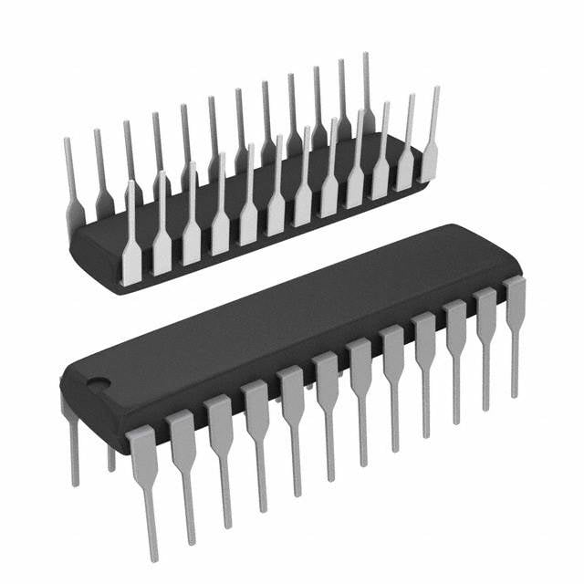
ICGOO在线商城 > 集成电路(IC) > 嵌入式 - CPLD(复杂可编程逻辑器件) > ATF750CL-15PU
- 型号: ATF750CL-15PU
- 制造商: Atmel
- 库位|库存: xxxx|xxxx
- 要求:
| 数量阶梯 | 香港交货 | 国内含税 |
| +xxxx | $xxxx | ¥xxxx |
查看当月历史价格
查看今年历史价格
ATF750CL-15PU产品简介:
ICGOO电子元器件商城为您提供ATF750CL-15PU由Atmel设计生产,在icgoo商城现货销售,并且可以通过原厂、代理商等渠道进行代购。 ATF750CL-15PU价格参考。AtmelATF750CL-15PU封装/规格:嵌入式 - CPLD(复杂可编程逻辑器件), 。您可以下载ATF750CL-15PU参考资料、Datasheet数据手册功能说明书,资料中有ATF750CL-15PU 详细功能的应用电路图电压和使用方法及教程。
| 参数 | 数值 |
| 产品目录 | 集成电路 (IC)半导体 |
| 描述 | IC CPLD 10MC 15NS 24DIPCPLD - 复杂可编程逻辑器件 750 GATE LOW POWER - 15NS |
| 产品分类 | |
| I/O数 | 10 |
| 品牌 | Atmel |
| 产品手册 | |
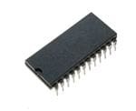
| 产品图片 |
|
| rohs | 符合RoHS无铅 / 符合限制有害物质指令(RoHS)规范要求 |
| 产品系列 | 嵌入式处理器和控制器,CPLD - 复杂可编程逻辑器件,Atmel ATF750CL-15PUATF750C(L) |
| 数据手册 | |
| 产品型号 | ATF750CL-15PU |
| 产品 | ATF750CL |
| 产品种类 | CPLD - 复杂可编程逻辑器件 |
| 供应商器件封装 | 24-PDIP |
| 其它名称 | ATF750CL15PU |
| 包装 | 管件 |
| 可编程类型 | 系统内可编程(最少 1K 次编程/擦除循环) |
| 商标 | Atmel |
| 大电池数量 | 10 |
| 存储类型 | EEPROM |
| 安装类型 | 通孔 |
| 安装风格 | Through Hole |
| 宏单元数 | 10 |
| 封装/外壳 | 24-DIP(0.300",7.62mm) |
| 封装/箱体 | PDIP-24 |
| 工作温度 | -40°C ~ 85°C |
| 工作电源电压 | 5 V |
| 工厂包装数量 | 15 |
| 延迟时间 | 15 ns |
| 延迟时间tpd(1)最大值 | 15.0ns |
| 最大工作温度 | + 85 C |
| 最大工作频率 | 71 MHz |
| 最小工作温度 | - 40 C |
| 栅极数 | - |
| 栅极数量 | 750 |
| 标准包装 | 15 |
| 每个宏指令的积项数 | 8 |
| 电源电压-内部 | 4.5 V ~ 5.5 V |
| 电源电压-最大 | 5.5 V |
| 电源电压-最小 | 4.5 V |
| 输入/输出端数量 | 10 |
| 逻辑元件/块数 | - |
| 逻辑数组块数量——LAB | - |





- 商务部:美国ITC正式对集成电路等产品启动337调查
- 曝三星4nm工艺存在良率问题 高通将骁龙8 Gen1或转产台积电
- 太阳诱电将投资9.5亿元在常州建新厂生产MLCC 预计2023年完工
- 英特尔发布欧洲新工厂建设计划 深化IDM 2.0 战略
- 台积电先进制程称霸业界 有大客户加持明年业绩稳了
- 达到5530亿美元!SIA预计今年全球半导体销售额将创下新高
- 英特尔拟将自动驾驶子公司Mobileye上市 估值或超500亿美元
- 三星加码芯片和SET,合并消费电子和移动部门,撤换高东真等 CEO
- 三星电子宣布重大人事变动 还合并消费电子和移动部门
- 海关总署:前11个月进口集成电路产品价值2.52万亿元 增长14.8%


PDF Datasheet 数据手册内容提取
Features • Advanced, High-speed, Electrically-erasable Programmable Logic Device – Superset of 22V10 – Enhanced Logic Flexibility – Backward Compatible with ATV750B/BL and ATV750/L (cid:129) Low-power Edge-sensing “L” Option with 1 mA Standby Current (cid:129) D- or T-type Flip-flop (cid:129) Product Term or Direct Input Pin Clocking for Flip-flop (cid:129) 7.5 ns Maximum Pin-to-pin Delay with 5V Operation High-speed (cid:129) Highest Density Programmable Logic Available in 24-pin and 28-pin Packages – Advanced Electrically-erasable Technology Complex – Reprogrammable – 100% Tested Programmable (cid:129) Increased Logic Flexibility – 42 Array Inputs, 20 Sum Terms and 20 Flip-flops Logic Device (cid:129) Enhanced Output Logic Flexibility – All 20 Flip-flops Feed Back Internally – 10 Flip-flops are also Available as Outputs ATF750C (cid:129) Programmable Pin-keeper Circuits (cid:129) Dual-in-line and Surface Mount Package in Standard Pinouts ATF750CL (cid:129) Full Military, Commercial and Industrial Temperature Ranges (cid:129) 20-year Data Retention (cid:129) 2000V ESD Protection (cid:129) 1000 Erase/Write Cycles (cid:129) Green Package Options (Pb/Halide-free/RoHS Compliant) Available 1. Block Diagram (OEPRODUCTTERMS) PROGRAMMABLE 12 INTERCONNECT LOGIC INPUT AND 4TO8 OPTION OUTPUT 10 PINS CLOOMGBIICNAATRORRAIYAL PRTEORDMUSCT (UPT020 OPTION PII/NOS FLIP-FLOPS) (CLOCKPIN) 0776L–PLD–11/08
2. Pin Configurations Pin Function CLK Clock IN Logic Inputs I/O Bi-directional Buffers GND Ground VCC +5V Supply 2.1 DIP/SOIC/TSSOP 2.2 PLCC/LCC CLK/IINN 12 2243 VI/OCC ININCLK/IN(1)VCCVCCI/OI/O IINN 34 2221 II//OO IN 5432128272625 I/O IN 5 20 I/O IN 6 24 I/O IN 6 19 I/O IN 7 23 I/O GND(1) 8 22 GND(1) IN 7 18 I/O IN 9 21 I/O IN 8 17 I/O IN 10 20 I/O IN 9 16 I/O IN 11 19 I/O IN 10 15 I/O 12131415161718 IN 11 14 I/O GND 12 13 IN ININGND(1)NDINI/OI/O G Note: For PLCC, pins 1, 8, 15, and 22 can be left uncon- nected. For superior performance, connect VCC to pin 1 and GND to pins 8, 15, and 22. 3. Description The ATF750C(L)s are twice as powerful as most other 24-pin programmable logic devices. Increased product terms, sum terms, flip-flops and output logic configurations translate into more usable gates. High-speed logic and uniform predictable delays guarantee fast in-system performance. The ATF750C(L) is a high-performance CMOS (electrically-eras- able) complex programmable logic device (CPLD) that utilizes Atmel’s proven electrically- erasable technology. Each of the ATF750C(L)’s 22 logic pins can be used as an input. Ten of these can be used as inputs, outputs or bi-directional I/O pins. Each flip-flop is individually configurable as either D- or T-type. Each flip-flop output is fed back into the array independently. This allows burying of all the sum terms and flip-flops. There are 171 total product terms available. There are two sum terms per output, providing added flexibility. A variable format is used to assign between four to eight product terms per sum term. Much more logic can be replaced by this device than by any other 24-pin PLD. With 20 sum terms and flip-flops, complex state machines are easily implemented with logic to spare. Product terms provide individual clocks and asynchronous resets for each flip-flop. Each flip-flop may also be individually configured to have direct input pin controlled clocking. Each output has its own enable product term. One product term provides a common synchronous preset for all flip-flops. Register preload functions are provided to simplify testing. All registers automatically reset upon power-up. The ATF750CL is a low-power device with speeds asfastas 15 ns. The ATF750CL provides the optimum low-power CPLD solution. This device significantly reduces total system power, thereby allowing battery-powered operations. ATF750C(L) 2 0776L–PLD–11/08
ATF750C(L) 4. Absolute Maximum Ratings* Temperature Under Bias................................-55°C to +125°C *NOTICE: Stresses beyond those listed under “Absolute Maximum Ratings” may cause permanent dam- Storage Temperature.....................................-65°C to +150°C age to the device. This is a stress rating only and functional operation of the device at these or any Voltage on Any Pin with other conditions beyond those indicated in the Respect to Ground.........................................-2.0V to +7.0V(1) operational sections of this specification is not implied. Exposure to absolute maximum rating Voltage on Input Pins conditions for extended periods may affect device with Respect to Ground reliability. During Programming.....................................-2.0V to +14.0V(1) Note: 1. Minimum voltage is -0.6V DC, which may under- shoot to -2.0V for pulses of less than 20 ns. Programming Voltage with Maximum output pin voltage is VCC + 0.75V DC, Respect to Ground.......................................-2.0V to +14.0V(1) which may overshoot to 7.0V for pulses of less than 20 ns. 5. DC and AC Operating Conditions All members of the family are specified to operate in either one of two voltage ranges. Parameters are specified as noted to be either 2.7V to 3.6V, 5V ±5% or 5V ±10%. Commercial Industrial 5V Operation -7.5, -10, -15 -10, -15 Military -55°C - +125°C Operating Temperature (Ambient) 0°C - 70°C -40°C - +85°C (case) V Power Supply 5V ± 5% 5V ± 10% 5V ± 10% CC 3 0776L–PLD–11/08
6. Logic Options Combinatorial Output Registered Output Combined Terms Separate Terms Combined Terms Separate Terms 7. Clock Mux CKMUX CKi TO LOGIC CLK CLOCK CELL PIN PRODUCT SELECT TERM 8. Output Options ATF750C(L) 4 0776L–PLD–11/08
ATF750C(L) 9. Bus-friendly Pin-keeper Input and I/Os All input and I/O pins on the ATF750C(L) have programmable “pin-keeper” circuits. If activated, when any pin is driven high or low and then subsequently left floating, it will stay at that previous high or low level. This circuitry prevents unused input and I/O lines from floating to intermediate voltage levels, which causes unnecessary power consumption and system noise. The keeper circuits eliminate the need for external pull-up resistors and eliminate their DC power consumption. Enabling or disabling of the pin-keeper circuits is controlled by the device type chosen in the logic compiler device selection menu. Please refer to the software compiler table for more details. Once the pin-keeper circuits are disabled, normal termination procedures are required for unused inputs and I/Os. 10. Input Diagram V CC INPUT 100K ESD PROTECTION CIRCUIT PROGRAMMABLE OPTION 11. I/O Diagram V CC OE DATA I/O V CC 100K PROGRAMMABLE OPTION 5 0776L–PLD–11/08
12. DC Characteristics Symbol Parameter Condition Min Typ Max Units I Input Load Current V = -0.1V to V + 1V 10 µA LI IN CC Output Leakage I V = -0.1V to V + 0.1V 10 µA LO Current OUT CC Com. 125 180 mA C-7, -10 Ind., Mil. 135 190 mA Power Supply VCC = Max, Com. 125 180 mA I V = Max, C-15 CC Current, Standby OIuNtputs Open Ind., Mil. 135 190 mA Com. 0.12 1 mA CL-15 Ind. 0.15 2 mA Output Short I (1) V = 0.5V -120 mA OS Circuit Current OUT V Input Low Voltage 4.5 ≤ V ≤ 5.5V -0.6 0.8 V IL CC V Input High Voltage 2.0 V + 0.75 V IH CC I = 16 mA Com., Ind. 0.5 V OL Output Low V = V or V , V IN IH IL I = 12 mA Mil. 0.5 V OL Voltage V = Min OL CC I = 24 mA Com. 0.8 V OL Output High V = V or V , V IN IH IL I = -4.0 mA 2.4 V OH Voltage V = Min OH CC Note: 1. Not more than one output at a time should be shorted. Duration of short circuit test should not exceed 30 sec. 13. Input Test Waveforms and Measurement Levels t , t < 3 ns (10% to 90%) R F 14. Output Test Load VCC 300 (390 MIL.) 390 (750 MIL.) ATF750C(L) 6 0776L–PLD–11/08
ATF750C(L) 15. AC Waveforms, Product Term Clock(1) Note: 1. Timing measurement reference is 1.5V. Input AC driving levels are 0.0V and 3.0V, unless otherwise specified. 16. AC Characteristics, Product Term Clock(1) -7 -10 C/CL-15 Symbol Parameter Min Max Min Max Min Max Units t Input or Feedback to Non-registered Output 7.5 10 15 ns PD t Input to Output Enable 7.5 10 15 ns EA t Input to Output Disable 7.5 10 15 ns ER t Clock to Output 3 7.5 4 10 5 12 ns CO t Clock to Feedback 1 5 4 7.5 5 9 ns CF t Input Setup Time 3 4 8/12 ns S t Feedback Setup Time 3 4 7 ns SF t Hold Time 1 2 5 ns H t Clock Period 7 11 14 ns P t Clock Width 3.5 5.5 7 ns W External Feedback 1/(t + t ) 95 71 50/41 MHz S CO f Internal Feedback 1/(t + t ) 125 86 62 MHz MAX SF CF No Feedback 1/(t ) 142 90 71 MHz P t Asynchronous Reset Width 5 10 15 ns AW t Asynchronous Reset Recovery Time 3 10 15 ns AR t Asynchronous Reset to Registered Output Reset 8 12 15 ns AP t Setup Time, Synchronous Preset 4 7 8 ns SP Note: 1. See ordering information for valid part numbers. 7 0776L–PLD–11/08
17. AC Waveforms, Input Pin Clock(1) Note: 1. Timing measurement reference is 1.5V. Input AC driving levels are 0.0V and 3.0V, unless otherwise specified. 18. AC Characteristics, Input Pin Clock -7 -10 C/CL-15 Symbol Parameter Min Max Min Max Min Max Units t Input or Feedback to Non-registered Output 7.5 10 15 ns PD t Input to Output Enable 7.5 10 15 ns EA t Input to Output Disable 7.5 10 15 ns ER t Clock to Output 0 6.5 0 7 0 10 ns COS t Clock to Feedback 0 3.5 0 5 0 5.5 ns CFS t Input Setup Time 4 5 8/12.5 ns SS t Feedback Setup Time 4 5 7 ns SFS t Hold Time 0 0 0 ns HS t Clock Period 7 10 12 ns PS t Clock Width 3.5 5 6 ns WS External Feedback 1/(t + t ) 95 83 55/44 MHz SS COS f Internal Feedback 1/(t + t ) 133 100 80 MHz MAXS SFS CFS No Feedback 1/(t ) 142 100 83 MHz PS t Asynchronous Reset Width 5 10 15 ns AW t Asynchronous Reset Recovery Time 5 10 15 ns ARS t Asynchronous Reset to Registered Output Reset 8 10 15 ns AP t Setup Time, Synchronous Preset 5 5/9 11 ns SPS ATF750C(L) 8 0776L–PLD–11/08
ATF750C(L) 19. Functional Logic Diagram ATF750C, Upper Half 9 0776L–PLD–11/08
20. Functional Logic Diagram ATF750C, Lower Half ATF750C(L) 10 0776L–PLD–11/08
ATF750C(L) 21. Power-up Reset The registers in the ATF750C(L)s are designed to reset during power-up. At a point delayed slightly from V crossing V , all registers will be reset to the low state. The output state will CC RST depend on the polarity of the output buffer. This feature is critical for state machine initialization. However, due to the asynchronous nature of reset and the uncertainty of how V actually rises in the system, the following conditions are CC required: 1. The V rise must be monotonic, CC 2. After reset occurs, all input and feedback setup times must be met before driving the clock terms or pin high, and 3. The clock pin, or signals from which clock terms are derived, must remain stable duringt . PR Parameter Description Typ Max Units t Power-up Reset Time 600 1000 ns PR V Power-up Reset Voltage 2.0 4.5 V RST 22. Pin Capacitance f = 1 MHz, T = 25°C(1) Typ Max Units Conditions C 5 8 pF V = 0V IN IN C 6 8 pF V = 0V OUT OUT Note: 1. Typical values for nominal supply voltage. This parameter is only sampled and is not 100% tested. 11 0776L–PLD–11/08
23. Using the ATF750C’s Many Advanced Features The ATF750C(L)’s advanced flexibility packs more usable gates into 24 pins than any other logic device. The ATF750C(L)s start with the popular 22V10 architecture, and add several enhanced features: (cid:129) Selectable D- and T-type Registers Each ATF750C(L) flip-flop can be individually configured as either D- or T-type. Using the T- type configuration, JK and SR flip-flops are also easily created. These options allow more efficient product term usage. (cid:129) Selectable Asynchronous Clocks Each of the ATF750C(L)’s flip-flops may be clocked by itsown clock product term or directly from Pin 1 (SMD Lead 2). This removes the constraint that all registers must use the same clock. Buried state machines, counters and registers can all coexist in one device while running on separate clocks. Individual flip-flop clock source selection further allows mixing higher performance pin clocking and flexible product term clocking within one design. (cid:129) A Full Bank of Ten More Registers The ATF750C(L) provides two flip-flops per output logic cell for a total of 20. Each register has its own sum term, its own reset term and its own clock term. (cid:129) Independent I/O Pin and Feedback Paths Each I/O pin on the ATF750C(L) has a dedicated input path. Each of the 20 registers has its own feedback terms into the array as well. This feature, combined with individual product terms for each I/O’s output enable, facilitates true bi-directional I/O design. 24. Synchronous Preset and Asynchronous Reset One synchronous preset line is provided for all 20 registers in the ATF750C(L). The appropriate input signals to cause the internal clocks to go to a high state must be received during a syn- chronous preset. Appropriate setup and hold times must be met, as shown in the switching waveform diagram. An individual asynchronous reset line is provided for each of the 20 flip-flops. Both master and slave halves of the flip-flops are reset when the input signals received force the internal resets high. 25. Software Support All family members of the ATF750C(L) can be designed with Atmel®-WinCUPL. Additionally, the ATF750C may be programmed to perform the ATV750(L) functional subset (no T-type flip-flops, pin clocking or D/T2 feedback) using the ATV750 JEDEC file. In this case, the ATF750C becomes a direct replacement or speed upgrade for the ATV750. The ATF750C is a direct replacement for the ATV750(L) and the ATV750B(L). ATF750C(L) 12 0776L–PLD–11/08
ATF750C(L) 26. Software Compiler Mode Selection Table 26-1. Software Compiler Mode Selection Device Atmel - WinCupL Device Mnemonic Pin-keeper V750C Disabled ATF750C-DIP V750CPPK Enabled V750LCC Disabled ATF750C-PLCC V750CPPKLCC Enabled 27. Third Party Programmer Support Table 27-1. Third Party Programmer Support Device Description V750 Cross-programming. JEDEC file compatible with standard V750 JEDEC file (total fuses in JEDEC file = 14394). The Programmer will automatically program “0”s into the User Rrow (UES), and disable the Pin-keeper features. The ATF750C (V750) Fuse Checksum will be the same as the old ATV750/L file. This device type is recommended for customers that are directly migrating from an ATV750/L device to an ATF750C/CL device. V750B Cross-programming. JEDEC file compatible with standard V750B JEDEC file (total fuses in JEDEC file = 14435). The Programmer will automatically program “0”s into the User Row (UES), and disable the Pin-keeper ATF750C (V750B) feature. The Fuse Checksum will be the same as the old ATV750B/BL file. This device type is recommended for customers that are directly migrating from an ATV750B/BL device to an ATF750C/CL device. Programming of User Row (UES) bits supported and Pin-keeper bit is user- programmable. (Total fuses in JEDEC file = 14504). This is the default device ATF750C type and is recommended for users that have re-compiled their source design files to specifically target the ATF750C device. Note: 1. The ATF750C has 14,504 JEDEC fuses. 28. Security Fuse Usage A single fuse is provided to prevent unauthorized copying of the ATF750C(L) fuse patterns. Once the security fuse isprogrammed, all fuses will appear programmed during verify. The security fuse should be programmed last, as its effect is immediate. 13 0776L–PLD–11/08
29. Preload of Registered Outputs The ATF750C(L)’s registers are provided with circuitry to allow loading of each register asyn- chronously with either a high or a low. This feature will simplify testing since any state can be forced into the registers to control test sequencing. A V level on the I/O pin will force the regis- IH ter high; a V will force it low, independent of the output polarity. The PRELOAD state is entered IL by placing a 10.25V to 10.75V signal on pin 8 on DIPs, and lead 10 on SMDs. When the clock term is pulsed high, the data on the I/O pins is placed into the register chosen by the select pin . Level Forced on Registered Select Pin Register #0 State Register #1 State Output Pin during Preload Cycle State after Cycle after Cycle V Low High X IH V Low Low X IL V High X High IH V High X Low IL ATF750C(L) 14 0776L–PLD–11/08
ATF750C(L) AATTFF775500CC S SUUPPPPLLYY C CUURRRREENNTT V VSS.. ATF750CL SUPPLY CURRENT SSUUPPPPLLYY V VOOLLTTAAGGEE ( T(TAA = = 2 255°°CC)) VS. SUPPLY VOLTAGE (TA = 25°C) 114400 160 112200 140 110000 120 mA)mA) 8800 A) 100 I (CCI (CC 46460000 I (µCC 6800 2200 40 00 20 44.5.500 44.7.755 55.0.000 55.2.255 55.5.500 0 SSUUPPPPLLYY V VOOLLTTAAGGEE ( V(V)) 4.50 4.75 5.00 5.25 5.50 SUPPLY VOLTAGE (V) SUPPLY CURRENT VS. FREQUENCY SUPPLY CURRENT VS. FREQUENCY STANDARD POWER (TA = 25°C) LOW-POWER ("L") VERSION (TA = 25°C) 160 140 120 120 100 A) A) 80 I (mCC 80 I (mCC 60 40 40 20 0 0 0 5 10 25 50 75 100 0 5 10 25 50 75 100 FREQUENCY (MHz) FREQUENCY (MHz) ATF750C/CL OUTPUT SOURCE CURRENT ATF750C/CL OUTPUT SOURCE CURRENT VS. SUPPLY VOLTAGE (V = 2.4V) OH VS. OUTPUT VOLTAGE (V = 5V, T = 25°C) CC A 0 0.00 -5 -10.00 -10 -20.00 -15 -30.00 I (mA)OH ---322050 I (mA)OH --5400..0000 -60.00 -35 -40 -70.00 -45 -80.00 -50 -90.00 4 4.5 5 5.5 6 0.00 0.50 1.00 1.50 2.00 2.50 3.00 3.50 4.00 4.50 5.00 SUPPLY VOLTAGE (V) VOH (V) 15 0776L–PLD–11/08
ATF750C/CL OUTPUT SINK CURRENT ATF750C/CL OUTPUT SINK CURRENT VS. SUPPLY VOLTAGE (VOL = 0.5V) VS. OUTPUT VOLTAGE (VCC = 5V, TA = 25°C) 44 140 43 120 42 41 100 A) 40 A) 80 I (mOL 3389 I (mOL 60 37 40 36 20 35 34 0 4 4.5 5 5.5 6 0 0.5 1 1.5 2 2.5 3 3.5 4 4.5 5 SUPPLY VOLTAGE (V) VOL (V) ATF750C/CL OUTPUT SINK CURRENT ATF750C/CL INPUT CURRENT VS. INPUT VOLTAGE VS. OUTPUT VOLTAGE (VCC = 5V, TA = 25°C) (VCC = 5V,TA = 25°C) 90 30 80 25 20 6700 T (uA) 1105 mA) 50 REN 5 I (OL 40 CUR 0 30 UT -5 P -10 20 IN -15 10 -20 0 -25 0 0.1 0.2 0.3 0.4 0.5 0.6 0.7 0.8 0.9 1 0 0.5 1 1.5 2 2.5 3 3.5 4 4.5 5 5.5 6 VOL (V) INPUT VOLTAGE (V) ATF750C/CL INPUT CURRENT VS. INPUT VOLTAGE ATF750C/CL INPUT CLAMP CURRENT (V = 5V,T = 25°C) CC A VS. INPUT VOLTAGE (V = 5V,T = 35°C) WITHOUT PIN-KEEPER CC A 1.8 0 1.6 -10 A) 1.4 mA) -20 INPUT CURRENT (u 00001.....246812 INPUT CURRENT ( -------98765430000000 0 -100 -0.2 0 -0.2 -0.4 -0.6 -0.8 -1 0 0.5 1 1.5 2 2.5 3 3.5 4 4.5 5 5.5 6 INPUT VOLTAGE (V) INPUT VOLTAGE (V) ATF750C(L) 16 0776L–PLD–11/08
ATF750C(L) 30. ATF750C(L) Military Ordering Information Ext. t t f PD COS MAXS (ns) (ns) (MHz) Ordering Code Package Operation Range ATF750C-10GM/883 24D3 ATF750C-10NM/883 28L 10 7 83 5962-0720101MLA 24D3 Military/883 5962-0720101M3A 28L (-55°C to 125°C) ATF750C-15GM/883 24D3 Class B, Fully Compliant ATF750C-15NM/883 28L 15 10 55 5962-0720102MLA 24D3 5962-0720102M3A 28L Note: 1. Special order only: TSSOP package requires special thermal management. 31. ATF750C(L) Green Package Options (Pb/Halide-free/RoHS Compliant) Ext. t t f PD COS MAXS (ns) (ns) (MHz) Ordering Code Package Operation Range ATF750C-7JX 28J Commercial 7.5 6.5 95 ATF750C-7PX 24P3 (0°C to 70°C) ATF750C-7SX 24S ATF750C-10JU 28J ATF750C-10PU 24P3 Industrial 10 7 83 ATF750C-10SU 24S (-40°C to 85°C) ATF750C-10XU 24X ATF750CL-15JU 28J ATF750CL-15PU 24P3 Industrial 15 10 44 ATF750CL-15SU 24S (-40°C to 85°C) ATF750CL-15XU 24X 32. Using “C” Product for Industrial To use commercial product for industrial ranges, down-grade one speed grade from the Industrial to the Commercial device (7 ns “X” = 10ns “U”) and de-rate power by 30%. Package Type 24D3 24-lead, 0.300" Wide, Non-windowed Ceramic Dual Inline Package (CerDIP) 28J 28-lead, Plastic J-leaded Chip Carrier (PLCC) 28L 28-pad, Non-Windowed Ceramic Leadless Chip Carrier (LCC) 24P3 24-lead, 0.300" Wide, Plastic Dual Inline Package (PDIP) 24S 24-lead, 0.300" Wide, Plastic Gull Wing Small Outline (SOIC) 24X(1) 24-lead, 0.173" Wide, Thin Shrink Small Outline (TSSOP) Note: 1. Special order only: TSSOP package requires special thermal management. 17 0776L–PLD–11/08
33. Packaging Information 33.1 24D3 – CerDIP Dimensions in Millimeters and (Inches). Controlling dimension: Inches. MIL-STD 1835 D-9 Config A (Glass Sealed) 32.51(1.280) 31.50(1.240) PIN 1 7.87(0.310) 7.24(0.285) 27.94(1.100) REF 5.08(0.200) 0.127(0.005)MIN MAX SEATING PLANE 1.52(0.060) 5.08(0.200) 0.38(0.015) 3.18(0.125) 0.66(0.026) 1.65(0.065) 0.36(0.014) 1.14(0.045) 2.45(0.100)BSC 8.13(0.320) 7.37(0.290) 0.46(0.018) 0º~ 15º REF 0.20(0.008) 10.20(0.400) MAX 10/21/03 TITLE DRAWING NO. REV. 2325 Orchard Parkway 24D3, 24-lead, 0.300" Wide. Non-windowed, Ceramic San Jose, CA 95131 24D3 B R Dual Inline Package (Cerdip) ATF750C(L) 18 0776L–PLD–11/08
ATF750C(L) 33.2 28J – PLCC 1.14(0.045) X 45˚ 1.14(0.045) X 45˚ PIN NO. 1 0.318(0.0125) IDENTIFIER 0.191(0.0075) E1 E B1 D2/E2 B e A2 D1 A1 D A 0.51(0.020)MAX 45˚ MAX (3X) COMMON DIMENSIONS (Unit of Measure = mm) SYMBOL MIN NOM MAX NOTE A 4.191 – 4.572 A1 2.286 – 3.048 A2 0.508 – – D 12.319 – 12.573 D1 11.430 – 11.582 Note 2 E 12.319 – 12.573 Notes: 1.This package conforms to JEDEC reference MS-018, Variation AB. E1 11.430 – 11.582 Note 2 2.Dimensions D1 and E1 do not include mold protrusion. Allowable protrusion is .010"(0.254 mm) per side. Dimension D1 D2/E2 9.906 – 10.922 and E1 include mold mismatch and are measured at the extreme B 0.660 – 0.813 material condition at the upper or lower parting line. 3. Lead coplanarity is 0.004" (0.102 mm) maximum. B1 0.330 – 0.533 e 1.270 TYP 10/04/01 TITLE DRAWING NO. REV. 2325 Orchard Parkway 28J, 28-lead, Plastic J-leaded Chip Carrier (PLCC) San Jose, CA 95131 28J B R 19 0776L–PLD–11/08
33.3 28L – LCC Dimensions in Millimeters and (Inches). Controlling dimension: Inches. MIL-STD 1835 C-4 11.68(0.460) 11.23(0.442) 2.54(0.100) 2.16(0.085) 11.68(0.460) 11.23(0.442) 1.91(0.075) 1.40(0.055) PIN 1 1.40(0.055) 1.14(0.045) INDEX CORNER 2.41(0.095) 1.91(0.075) 0.635(0.025) X 45˚ 0.381(0.015) 0.305(0.012) RADIUS 0.178(0.007) 7.62(0.300) BSC 0.737(0.029) 0.533(0.021) 1.27(0.050) TYP 1.02(0.040) X 45˚ 2.16(0.085) 7.62(0.300) BSC 1.65(0.065) 10/21/03 TITLE DRAWING NO. REV. 2325 Orchard Parkway 28L, 28-pad, Non-windowed, Ceramic Lid, Leadless Chip San Jose, CA 95131 28L B R Carrier (LCC) ATF750C(L) 20 0776L–PLD–11/08
ATF750C(L) 33.4 24P3 – PDIP D PIN 1 E1 A SEATING PLANE A1 L B B1 e E COMMON DIMENSIONS (Unit of Measure = mm) C SYMBOL MIN NOM MAX NOTE eC eB A – – 5.334 A1 0.381 – – D 31.623 – 32.131 Note 2 E 7.620 – 8.255 E1 6.096 – 7.112 Note 2 B 0.356 – 0.559 Notes: 1. This package conforms to JEDEC reference MS-001, Variation AF. B1 1.270 – 1.651 2. Dimensions D and E1 do not include mold Flash or Protrusion. Mold Flash or Protrusion shall not exceed 0.25 mm (0.010"). L 2.921 – 3.810 C 0.203 – 0.356 eB – – 10.922 eC 0.000 – 1.524 e 2.540 TYP 6/1/04 TITLE DRAWING NO. REV. 2325 Orchard Parkway 24P3, 24-lead (0.300"/7.62 mm Wide) Plastic Dual R San Jose, CA 95131 Inline Package (PDIP) 24P3 D 21 0776L–PLD–11/08
33.5 24S – SOIC B D1 D PIN 1 ID PIN 1 e E A COMMON DIMENSIONS (Unit of Measure = mm) SYMBOL MIN NOM MAX NOTE A1 A – – 2.65 A1 0.10 – 0.30 D 10.00 – 10.65 D1 7.40 – 7.60 0º ~ 8º E 15.20 – 15.60 L1 B 0.33 – 0.51 L 0.40 – 1.27 L L1 0.23 – 0.32 e 1.27 BSC 06/17/2002 TITLE DRAWING NO. REV. 2325 Orchard Parkway San Jose, CA 95131 24S, 24-lead (0.300" body) Plastic Gull Wing Small Outline (SOIC) 24S B R ATF750C(L) 22 0776L–PLD–11/08
ATF750C(L) 33.6 24X – TSSOP Dimensions in Millimeter and (Inches)* JEDEC STANDARD MO-153 AD Controlling dimension: millimeters 0.30(0.012) 0.19(0.007) 4.48(0.176) 6.50(0.256) 4.30(0.169) 6.25(0.246) PIN 1 0.65(0.0256)BSC 7.90(0.311) 7.70(0.303) 1.20(0.047)MAX 0.15(0.006) 0.05(0.002) 0.20(0.008) 0º ~ 8º 0.09(0.004) 0.75(0.030) 0.45(0.018) 04/11/2001 TITLE DRAWING NO. REV. 2325 Orchard Parkway 24X, 24-lead (4.4 mm body width) Plastic Thin Shrink Small Outline R San Jose, CA 95131 Package (TSSOP) 24X A 23 0776L–PLD–11/08
34. Revision History Revision Level – Release Date History Added military-grade devices. K – July 2007 Added fully-green RoHS-compliant devices in select speed grades and packages. L – November 2008 Removed commercial grade leaded package options. ATF750C(L) 24 0776L–PLD–11/08
Headquarters International Atmel Corporation Atmel Asia Atmel Europe Atmel Japan 2325 Orchard Parkway Unit 1-5 & 16, 19/F Le Krebs 9F, Tonetsu Shinkawa Bldg. San Jose, CA 95131 BEA Tower, Millennium City 5 8, Rue Jean-Pierre Timbaud 1-24-8 Shinkawa USA 418 Kwun Tong Road BP 309 Chuo-ku, Tokyo 104-0033 Tel: 1(408) 441-0311 Kwun Tong, Kowloon 78054 Saint-Quentin-en- Japan Fax: 1(408) 487-2600 Hong Kong YvelinesCedex Tel: (81) 3-3523-3551 Tel: (852) 2245-6100 France Fax: (81) 3-3523-7581 Fax: (852) 2722-1369 Tel: (33) 1-30-60-70-00 Fax: (33) 1-30-60-71-11 Product Contact Web Site Technical Support Sales Contact www.atmel.com pld@atmel.com www.atmel.com/contacts Literature Requests www.atmel.com/literature Disclaimer: The information in this document is provided in connection with Atmel products. No license, express or implied, by estoppel or otherwise,to any intellectualproperty right is granted by this document or in connection with the sale of Atmel products. EXCEPT AS SET FORTH IN ATMEL’S TERMS AND CONDI- TIONS OF SALE LOCATED ON ATMEL’S WEB SITE, ATMEL ASSUMES NO LIABILITY WHATSOEVER AND DISCLAIMS ANY EXPRESS, IMPLIED OR STATUTORY WARRANTY RELATING TO ITS PRODUCTS INCLUDING, BUT NOT LIMITED TO, THE IMPLIED WARRANTY OF MERCHANTABILITY, FITNESS FOR A PARTICULAR PURPOSE, OR NON-INFRINGEMENT. IN NO EVENT SHALL ATMEL BE LIABLE FOR ANY DIRECT, INDIRECT, CONSEQUENTIAL, PUNITIVE, SPECIAL OR INCIDEN- TAL DAMAGES (INCLUDING, WITHOUT LIMITATION, DAMAGES FOR LOSS OF PROFITS, BUSINESS INTERRUPTION, OR LOSS OF INFORMATION) ARISING OUT OF THE USE OR INABILITY TO USE THIS DOCUMENT, EVEN IF ATMEL HAS BEEN ADVISED OF THE POSSIBILITY OF SUCH DAMAGES. Atmel makes no representationsor warranties with respect to the accuracy or completeness of the contents of this document and reserves the right to make changes to specifications and product descriptions at any time without notice. Atmel does not make any commitment to update the information contained herein. Unless specifically provided otherwise, Atmel products are not suitable for, and shall not be used in, automotive applications. Atmel’s products are not intended, authorized, or warranted for use as components in applications intended to support or sustainlife. © 2008 Atmel Corporation. All rights reserved. Atmel®, Atmel logo and combinations thereof, and others are registered trademarks or trade- marks of Atmel Corporation or its subsidiaries. Other terms and product names may be trademarks of others. 0776L–PLD–11/08
Mouser Electronics Authorized Distributor Click to View Pricing, Inventory, Delivery & Lifecycle Information: M icrochip: ATF750C-10JU ATF750C-10PU ATF750C-10SU ATF750C-7JX ATF750C-7PX ATF750CL-15JU ATF750CL-15PU ATF750CL-15SU ATF750CL-15XU ATF750C-10GM/883 ATF750C-10NM/883 ATF750C-15GM/883 ATF750C- 15NM/883 ATF750C-7SX
 Datasheet下载
