ICGOO在线商城 > 射频/IF 和 RFID > RF 发射器 > ATA8405C-6DQY-66

 Datasheet下载
- 型号: ATA8405C-6DQY-66
- 制造商: Atmel
- 库位|库存: xxxx|xxxx
- 要求:
| 数量阶梯 | 香港交货 | 国内含税 |
| +xxxx | $xxxx | ¥xxxx |
查看当月历史价格
查看今年历史价格
ATA8405C-6DQY-66产品简介:
ICGOO电子元器件商城为您提供ATA8405C-6DQY-66由Atmel设计生产,在icgoo商城现货销售,并且可以通过原厂、代理商等渠道进行代购。 ATA8405C-6DQY-66价格参考。AtmelATA8405C-6DQY-66封装/规格:RF 发射器, RF Transmitter ASK, FSK 433MHz 6dBm 40kbps PCB, Surface Mount Antenna 10-TFSOP, 10-MSOP (0.118", 3.00mm Width)。您可以下载ATA8405C-6DQY-66参考资料、Datasheet数据手册功能说明书,资料中有ATA8405C-6DQY-66 详细功能的应用电路图电压和使用方法及教程。
| 参数 | 数值 |
| 产品目录 | |
| 描述 | IC TX UHF 433MHZ |
| 产品分类 | |
| 品牌 | Atmel |
| 数据手册 | |
| 产品图片 |
|
| 产品型号 | ATA8405C-6DQY-66 |
| rohs | 无铅 / 符合限制有害物质指令(RoHS)规范要求 |
| 产品系列 | - |
| 其它名称 | ATA8405C-6DQY-66DKR |
| 功率-输出 | 6dBm |
| 包装 | Digi-Reel® |
| 天线连接器 | PCB,表面贴装 |
| 存储容量 | - |
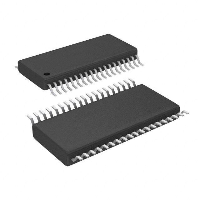
| 封装/外壳 | 10-TFSOP,10-MSOP(0.118",3.00mm 宽) |
| 工作温度 | -40°C ~ 85°C |
| 应用 | RKE,遥控系统 |
| 数据接口 | PCB,表面贴装 |
| 数据速率(最大值) | 40kbps |
| 标准包装 | 1 |
| 特性 | - |
| 电压-电源 | 1.9 V ~ 3.6 V |
| 电流-传输 | 8.5mA |
| 调制或协议 | ASK,FSK |
| 频率 | 433MHz |


PDF Datasheet 数据手册内容提取
ATA8404/ATA8405 UHF ASK/FSK Transmitter DATASHEET Features ● PLL transmitter IC with single-ended output ● High output power (6dBm) ● Low current consumption at 8.1mA (315MHz) and 8.5mA (433MHz) ● Divide by 24 (Atmel® ATA8404) and 32 (Atmel ATA8405) blocks for 13MHz crystal frequencies and for low XTO start-up times ● ASK/FSK modulation with internal FSK switch ● Up to 20Kbps manchester coding, up to 40Kbps NRZ coding ● Power-down ● ENABLE input for parallel usage of controlling pins ● Supply voltage range: 1.9V to 3.6V ● ESD protection at all pins (4kV HBM) ● Small package TSSOP10 Benefits ● Low parasitic FSK switch integrated ● Fast settling time <0.85ms ● Small form factor Applications ● Remote control systems ● Alarm, telemetering, and energy metering systems ● Home entertainment and home automation ● Industrial/aftermarket remote keyless entry systems ● Toys 9136H-AUTO-08/15
1. Description The Atmel® ATA8404/ATA8405 is a PLL transmitter IC, which has been developed for the demands of RF low-cost transmission systems at data rates up to 20kBaud Manchester coding and 40kBaud NRZ coding. The transmitting frequency range is 313MHz to 317MHz (Atmel ATA8404) and 432MHz to 448MHz (Atmel ATA8405), respectively. It can be used in both FSK and ASK systems. Figure 1-1. System Block Diagram UHF ASK/FSK TPM and Remote control UHF ASK/FSK transmitter Remote control receiver 1 Li cell ATA8404 ATA8201 ATA8405 ATA8202 1 to 3 Micro- ATA8203 Demod Control controller ATA8204 Encoder PLL ATARx9x Keys IF Amp Antenna Antenna XTO VCO PLL XTO Power LNA VCO amp. 2 ATA8404/ATA8405 [DATASHEET] 9136H–AUTO–08/15
2. Pin Configuration Figure 2-1. Pinning TSSOP10 CLK 1 10 ENABLE ASK 2 9 GND ATA8404 FSK 3 ATA8405 8 VS ANT2 4 7 XTO1 ANT1 5 6 XTO2 Table 2-1. Pin Description Pin Symbol Function Configuration VS Clock output signal for the microcontroller. The clock output frequency is set by the crystal to f /8. XTAL The CLK output stays Low in 100Ω 1 CLK power-down mode and after CLK enabling of the PLL. The CLK output switches on if 100Ω the oscillation amplitude of the crystal has reached a certain level. 200kΩ ASK 50kΩ V = 1.1V Switches on the power amplifier REF for ASK modulation and enables 2 ASK the PLL and XTO if the ENABLE 200kΩ pin is open. 20μA FSK 200kΩ V = 1.1V REF Switches off the FSK switch (switch has high Z if signal at pin 3 FSK FSK is High) and enables the 5μA PLL and the XTO if the ENABLE pin is open 200kΩ ATA8404/ATA8405 [DATASHEET] 3 9136H–AUTO–08/15
Table 2-1. Pin Description (Continued) Pin Symbol Function Configuration 4 ANT2 Emitter of antenna output stage ANT1 5 ANT1 Open collector antenna output ANT2 210μA (FSK < 0.25V) and Diode switch, used for FSK 6 XTO2 (ENABLE > 1.7V) modulation XT02 VS VS 1.5kΩ 1.2kΩ 7 XTO1 Connection for crystal XTO1 182μA 8 VS Supply voltage See ESD protection circuitry (see Figure 4-9 on page 12) 9 GND Ground See ESD protection circuitry (see Figure 4-9 on page 12) VS ENABLE input 30μA If ENABLE is connected to GND (FSK > 1.7V) and the ASK or FSK pin is High, 10 ENABLE or the device stays in idle mode. (ASK > 1.7V) In normal operation ENABLE is ENABLE 150kΩ left open and ASK or FSK is used to enable the device. 250kΩ 4 ATA8404/ATA8405 [DATASHEET] 9136H–AUTO–08/15
Figure 2-2. Block Diagram ATA8405 Power up/down EN f CLK ENABLE 1 8 10 f 24/ 32 ASK GND 2 9 OR PDF FSK VS 3 8 CP Ampl. OK ANT2 XTO XTO1 4 LF 7 EN ANT1 PA VCO XTO2 5 6 PLL 3. General Description This fully integrated PLL transmitter allows the design of simple, low-cost RF miniature transmitters for remote control and other industrial applications. The VCO is locked to 24f /32f for Atmel® ATA8404/ATA8405. Thus, a XTAL XTAL 13.125MHz/13.56MHz crystal is needed for a 315MHz/433.92MHz transmitter. All other PLL and VCO peripheral elements are integrated. The XTO is a series resonance (current mode) oscillator. Only one capacitor and a crystal connected in series to GND are needed as external elements in an ASK system. The internal FSK switch, together with a second capacitor, can be used for FSK modulation. The crystal oscillator needs typically 0.6ms until the CLK output is activated if a crystal as defined in the electrical characteristics is used (e.g., TPM crystal). For most crystals used in RKE systems, a shorter time will result. The CLK output is switched on if the amplitude of the current flowing through the crystal has reached 35% to 80% of its final value. This is synchronized with the 1.64/1.69MHz CLK output. As a result, the first period of the CLK output is always a full period. The PLL is then locked <250µs after CLK output activation. This means an additional wait time of 250µs is necessary before the PA can be switched on and the data transmission can start. This results in a significantly lower time of about 0.85ms between enabling the Atmel ATA8404/ATA8405 and the beginning of the data transmission which saves battery power. The power amplifier is an open-collector output delivering a current pulse which is nearly independent from the load impedance and can therefore be controlled via the connected load impedance. This output configuration enables a simple matching to any kind of antenna or to 50. A high power efficiency for the power amplifier results if an optimized load impedance of Z =380+j340 (Atmel ATA8404) at 315MHz and Load,opt Z =280+j310 (Atmel ATA8405) at 433.92MHz is used at the 3-V supply voltage. Load,opt ATA8404/ATA8405 [DATASHEET] 5 9136H–AUTO–08/15
4. Functional Description If ASK=Low, FSK=Low, and ENABLE=open or Low, the circuit is in power-down mode consuming only a very small amount of current so that a lithium cell used as power supply can work for many years. If the ENABLE pin is left open, ENABLE is the logical OR operation of the ASK and FSK input pins. This means, the IC can be switched on by either the FSK of the ASK input. If the ENABLE pin is Low and ASK or FSK are High, the IC is in idle mode where the PLL, XTO, and power amplifier are off and the microcontroller ports controlling the ASK and FSK inputs can be used to control other devices. This can help to save ports on the microcontroller in systems where other devices with 3-wire interface are used. With FSK=High, ASK=Low, and ENABLE=open or High, the PLL and the XTO are switched on and the power amplifier is off. When the amplitude of the current through the crystal has reached 35%to80% of its final amplitude, the CLK driver is automatically activated. The CLK output stays Low until the CLK driver has been activated. The driver is activated synchronously with the CLK output frequency, hence, the first pulse on the CLK output is a complete period. The PLL is then locked within <250µs after the CLK driver has been activated, and the transmitter is then ready for data transmission. With ASK=High, the power amplifier is switched on. This is used to perform the ASK modulation. During ASK modulation, the IC is enabled with the FSK or the ENABLE pin. With FSK=Low the switch at pin XTO2 is closed, with FSK=High the switch is open. To achieve a faster start-up of the crystal oscillator, the FSK pin should be High during start-up of the XTO because the series resistance of the resonator seen from pin XTO1 is lower if the switch is off. The different modes of the Atmel® ATA8404/ATA8405 are listed in Table 4-1, the corresponding current consumption values can be found in the table “Electrical Characteristics” on page 13. Table 4-1. Atmel ATA8404/ATA8405 Modes ASK Pin FSK Pin ENABLE Pin Mode Low Low Low/open Power-down mode, FSK switch High Z Low Low High Power-up, PA off, FSK switch Low Z Low High High/open Power-up, PA off, FSK switch High Z High Low High/open Power-up, PA on, FSK switch Low Z High High High/open Power-up, PA on, FSK switch High Z Low/High High Low Idle mode, FSK switch High Z High Low/High Low Idle mode, FSK switch High Z 4.1 Transmission with ENABLE = open 4.1.1 ASK Mode The Atmel ATA8404/ATA8405 is activated by ENABLE = open, FSK=High, ASK=Low. The microcontroller is then switched to external clocking. After typically 0.6ms, the CLK driver is activated automatically (i.e., the microcontroller waits until the XTO and CLK are ready). After another time period of 250µs, the PLL is locked and ready to transmit. The output power can then be modulated by means of pin ASK. After transmission, ASK is switched to Low and the microcontroller returns back to internal clocking. Then, the Atmel ATA8404/ATA8405 is switched to power-down mode with FSK=Low. 6 ATA8404/ATA8405 [DATASHEET] 9136H–AUTO–08/15
Figure 4-1. Timing ASK Mode with ENABLE not Connected to the Microcontroller Δ T > 250 μs XTO FSK ASK CLK Power-down Power-up, Power-up, Power-up, Power-down PA off PA on PA off (High) (Low) 4.1.2 FSK Mode The Atmel® ATA8404/ATA8405 is activated by FSK=High, ASK=Low. The microcontroller is then switched to external clocking. After typically 0.6ms, the CLK driver is activated automatically (i.e., the microcontroller waits until the XTO and CLK are ready. After another time period of 250µs, the PLL is locked and ready to transmit. The power amplifier is switched on with ASK=H. The Atmel ATA8404/ATA8405 is then ready for FSK modulation. The microcontroller starts to switch on and off the capacitor between the crystal load capacitor and GND by means of pin FSK, thus, changing the reference frequency of the PLL. IF FSK=L the output frequency is lower; if FSK=H the output frequency is higher. After transmission, FSK stays High and ASK is switched to Low and the microcontroller returns back to internal clocking. Then, the ATA8404/ATA8405 is switched to power-down mode with FSK=Low. Figure 4-2. Timing FSK Mode with ENABLE not Connected to the Microcontroller Δ T > 250 μs XTO FSK ASK CLK Power-down Power-up, Power-up, Power-up, Power-down PA off PA on PA off (f = High) (f = Low) RF RF 4.2 Transmission with ENABLE = High 4.2.1 FSK Mode The Atmel ATA8404/ATA8405 is activated by ENABLE=High, FSK=High, and ASK=Low. The microcontroller is then switched to external clocking. After typically 0.6ms, the CLK driver is activated automatically (i.e., the microcontroller waits until the XTO and CLK are ready). After another time period of 250µs, the PLL is locked and ready to transmit. The power amplifier is switched on with ASK=H. The Atmel ATA8404/ATA8405 is then ready for FSK modulation. The microcontroller starts to switch on and off the capacitor between the crystal load capacitor and GND by means of pin FSK, thus, changing the reference frequency of the PLL. IF FSK=L the output frequency is lower, if FSK=H output frequency is higher. After transmission, ASK is switched to Low and the microcontroller returns back to internal clocking. Then, the Atmel ATA8404/ATA8405 is switched to power-down mode with ENABLE=Low and FSK=Low. ATA8404/ATA8405 [DATASHEET] 7 9136H–AUTO–08/15
Figure 4-3. Timing FSK Mode with ENABLE Connected to the Microcontroller Δ T > 250 μs XTO ENABLE FSK ASK CLK Power-down Power-up, Power-up, Power-up, Power-down PA off PA on PA off (f = High) (f = Low) RF RF 4.2.2 ASK Mode The Atmel ATA8404/ATA8405 is activated by ENABLE=High, FSK=High and ASK=Low. After activation the microcontroller is switched to external clocking. After typically 0.6ms, the CLK driver is activated automatically (the microcontroller waits until the XTO and CLK are ready). After another time period of 250µs, the PLL is locked and ready to transmit. The output power can then be modulated by means of pin ASK. After transmission, ASK is switched to Low and the microcontroller returns back to internal clocking. Then, the Atmel ATA8404/ATA8405 is switched to power-down mode with ENABLE=Low and FSK=Low. Figure 4-4. Timing ASK Mode with ENABLE Connected to the Microcontroller Δ T > 250 μs XTO ENABLE FSK ASK CLK Power-down Power-up, Power-up, Power-up, Power-down PA off PA on PA off (High) (Low) 8 ATA8404/ATA8405 [DATASHEET] 9136H–AUTO–08/15
4.3 Accuracy of Frequency Deviation The accuracy of the frequency deviation using the XTAL pulling method is about ±20% if the following tolerances are considered. One important aspect is that the values of C and C of typical crystals are strongly correlated, which reduces 0 M the tolerance of the frequency deviation. Figure 4-5. Tolerances of Frequency Modulation VS CStray LM C4 XTAL CM RS C0 C5 Crystal equivalent circuit CSwitch Using a crystal with a motional capacitance of C =4.37fF ±15%, a nominal load capacitance of C =18pF and a parallel M LNOM capacitance of C =1.30pF correlated with C results in C =297C the correlation has a tolerance of 10%, so C =267 0 M 0 M 0 to 326C ). If using the internal FSK switch with C =0.9pF ±20% and estimated parasitics of C =0.7pF ±10%, the M Switch Stray resulting C and C values are C =10pF ±1% and C =15pF ±1% for a nominal frequency deviation of ±19.3kHz with worst 4 5 4 5 case tolerances of ±15.8kHz to ±23.2kHz. 4.4 Accuracy of the Center Frequency The imaginary part of the impedance in large signal steady state oscillation IM ,seen into the pin7 (XTO1), causes some XTO additional frequency tolerances, due to pulling of the XTO oscillation frequency. These tolerances have to be added to the tolerances of the crystal itself (adjustment tolerance, temperature stability and ageing) and the impact on the center frequency due to tolerances of C , C , C and C . The nominal value of IM =110, C and C should be 4 5 Switch Stray XTO Switch Stray absorbed into the C and C values by using a crystal with known frequency and choosing C and C , so that the XTO center 4 5 4 5 frequency equals the crystal frequency, and the frequency deviation is as expected. Then, from the nominal value, the IM XTO has ±90 tolerances, using the pulling formula P=–IM C f with f =13.56MHz and C =4.4fF an XTO M XTO XTO M additional frequency tolerance of P=±16.86ppm results. If using crystals with other C the additional frequency tolerance M can be calculated in the same way. For example, a lower C =3.1fF will reduce the frequency tolerance to 11.87ppm, where M a higher C =5.5fF increases the tolerance to 21.07ppm. M 4.5 CLK Output An output CLK signal of 1.64MHz (Atmel® ATA8404 operating at 315MHz) and 1.69MHz (Atmel ATA8405 operating at 433.92MHz) is provided for a connected microcontroller. The delivered signal is CMOS-compatible with a High and Low time of >125ns if the load capacitance is lower than 20pF. The CLK output is Low in power-down mode due to an internal pull- down resistor. After enabling the PLL and XTO the signal stays Low until the amplitude of the crystal oscillator has reached 35% to 80% of its amplitude. Then, the CLK output is activated synchronously with its output signal so that the first period of the CLK output signal is a full period. 4.5.1 Clock Pulse Take-over by Microcontroller The clock of the crystal oscillator can be used for clocking the microcontroller. Atmel’s ATARx9x microcontroller family provides the special feature of starting with an integrated RC oscillator to switch on the Atmel ATA8404/ATA8405’s external clocking and to wait automatically until the CLK output of the Atmel ATA8404/ATA8405 is activated. After a time period of 250µs the message can be sent with crystal accuracy. ATA8404/ATA8405 [DATASHEET] 9 9136H–AUTO–08/15
4.5.2 Output Matching and Power Setting The output power is set by the load impedance of the antenna. The maximum output power is achieved with a load impedance of Z =380+j340 (Atmel ATA8404) at 315MHz and Z =280+j310 (Atmel ATA8405) at Load,opt Load,opt 433.92MHz. A low resistive path to V is required to deliver the DC current (see Figure 4-6 on page 10). S The power amplifier delivers a current pulse and the maximum output power is delivered to a resistive load if the 0.66pF output capacitance of the power amplifier is compensated by the load impedance. At the ANT1 pin, the RF output amplitude is about V – 0.5V. S The load impedance is defined as the impedance seen from the ATA8404’s ANT1, ANT2 into the matching network. Do not mix up this large-signal load impedance with a small-signal input impedance delivered as an input characteristic of RF amplifiers. The latter is measured from the application into the IC instead of from the IC into the application for a power amplifier. The output capacitance of 0.66pF will be absorbed into the load impedance, so a real impedance of 684 (Atmel® ATA8404) at 315MHz and 623 (Atmel ATA8405) at 433.92MHz should be measured with a network analyses at pin5 (ANT1) with the Atmel ATA8404/ATA8405 soldered, an optimized antenna connected, and the power amplifier switched off. Less output power is achieved by lowering the real parallel part where the parallel imaginary part should be kept constant. Lowering the real part of the load impedance also reduces the supply voltage dependency of the output power. Output power measurement can be done with the circuit as shown in Figure 4-6. Please note that the component values must be changed to compensate for the individual board parasitics until the Atmel ATA8404/ATA8405 has the right load impedance. Also, the damping of the cable used to measure the output power must be calibrated. Figure 4-6. Output Power Measurement Atmel ATA8404/ATA8405 VS C1 = 1 nF L1 = 68 nH/ 39 nH Power meter ANT1 Z = 50Ω ZLopt C2 = 2.2 pF/ 1.8 pF Rin 50Ω ANT2 Table 4-2 and Table 4-3 show the output power and the supply current versus temperature and supply voltage. Table 4-2. Output Power and Supply Current versus Temperature and Supply Voltage for the Atmel ATA8404 with Z =380+j340 (Correlation Tested) Load V = 2.0V V = 3.0V V = 3.6V S S S Ambient Temperature (dBm/mA) (dBm/mA) (dBm/mA) T = 0°C 3.1 ±1.5 / 7.2 6.1 +2/–3 / 7.7 7.1 +2/–3 / 7.9 amb T = +25°C 3.0 ±1.5 / 7.5 6.0 ±2 / 8.1 7.4 ±2 / 8.3 amb T = +50°C 3.0 ±1.5 / 7.5 5.8 +2/–3 / 8.2 7.2 +2/–3 / 8.5 amb Table 4-3. Output Power and Supply Current versus Temperature and Supply Voltage for the Atmel ATA8405 with Z =280+j310 (Correlation Tested) Load V = 2.0V V = 3.0V V = 3.6V S S S Ambient Temperature (dBm/mA) (dBm/mA) (dBm/mA) T = 0°C 3.3 ±1.5 / 7.6 6.2 +2/–3 / 8.1 7.1 +2/–3 / 8.4 amb T = +25°C 3.0 ±1.5 / 8.0 6.0 ±2 / 8.5 7.5 ±2 / 8.8 amb T = +50°C 2.8 ±1.5 / 8.0 5.7 +2/–3 / 8.6 6.8 +2/–3 / 8.8 amb 10 ATA8404/ATA8405 [DATASHEET] 9136H–AUTO–08/15
4.6 Application Circuits For the supply voltage blocking capacitor C , a value of 68nF/X7R is recommended (see Figure 4-7 on page 11 and Figure 3 4-8 on page 12). C and C are used to match the loop antenna to the power amplifier. For C , two capacitors in series 1 2 2 should be used to achieve a better tolerance value and to enable it to realize Z by using capacitors with standard Load,opt values. Together with the pins of Atmel® ATA8404 and the PCB board wires, C a series resonance loop that suppresses the 1st 1 forms harmonic, hence the position of C on the PCB is important. Normally, the best suppression is achieved when C is placed 1 1 as close as possible to the pins ANT1 and ANT2. The loop antenna should not exceed a width of 1.5mm, otherwise the Q-factor of the loop antenna is too high. L (50nH to 100nH) can be printed on the PCB. C should be selected so that the XTO runs on the load resonance frequency 1 4 of the crystal. Normally, a value of 10pF results in a 12pF load-capacitance crystal due to the board parasitic capacitances and the inductive impedance of the XTO1 pin. Figure 4-7. ASK Application Circuit S1 BPXY VDD AVR® (ATtiny) VS 1 S2 BPXY VSS 20 BPXY OSC1 BPXY 7 ATA8404 ATA8405 Power up/down EN CLK f ENABLE 1 8 10 f 24/ ASK 32 GND 2 9 C3 OR PDF FSK VS 3 8 CP VS C2 Ampl. OK ANT2 XTO1 XTAL XTO 4 LF 7 Loop Antenna C1 C4 EN ANT1 XTO2 PA VCO 5 6 PLL L1 VS ATA8404/ATA8405 [DATASHEET] 11 9136H–AUTO–08/15
Figure 4-8. FSK Application Circuit S1 BPXY VDD AVR® (ATtiny) VS 1 S2 BPXY VSS 20 BPXY OSC1 BPXY 7 ATA8404 ATA8405 Power up/down EN CLK f ENABLE 1 8 10 f 24/ ASK 32 GND 2 9 C3 OR PDF FSK VS 3 8 CP VS C2 Ampl. OK ANT2 XTO1 XTAL XTO 4 LF 7 Loop Antenna C1 EN ANT1 XTO2 C5 PA VCO 5 6 PLL L1 C4 VS Figure 4-9. ESD Protection Circuit VS ANT1 CLK ASK FSK ANT2 XTO2 XTO1 ENABLE GND 12 ATA8404/ATA8405 [DATASHEET] 9136H–AUTO–08/15
5. Absolute Maximum Ratings Stresses beyond those listed under “Absolute Maximum Ratings” may cause permanent damage to the device. This is a stress rating only and functional operation of the device at these or any other conditions beyond those indicated in the operational sections of this specification is not implied. Exposure to absolute maximum rating conditions for extended periods may affect device reliability. Parameters Symbol Minimum Maximum Unit Supply voltage V 5 V S Power dissipation P 100 mW tot Junction temperature T 150 °C j Storage temperature T –55 +85 °C stg Ambient temperature T –55 +85 °C amb1 Ambient temperature in power-down mode for 15 minutes without damage with V 3.2V S T 175 °C V <0.25V or ENABLE is open, amb2 ENABLE V <0.25V, V <0.25V ASK FSK Input voltage V –0.3 (V + 0.3)(1) V maxASK S Note: 1. If V + 0.3 is higher than 3.7V, the maximum voltage will be reduced to 3.7V. S 6. Thermal Resistance Parameters Symbol Value Unit Junction ambient R 170 K/W thJA 7. Electrical Characteristics V = 3.0V and T = 25°C. All parameters are referred to GND (pin 9). S amb C =4.37fF, C =1.3pF, C =18pF, C =10pF, C =15pF and R 60 M 0 LNOM 4 5 S Parameters Test Conditions Symbol Min. Typ. Max. Unit Supply voltage V 1.9 3.6 V S Ambient temperature T 0 +50 °C amb V <0.25V or ENABLE is open, ENABLE Supply current, V <0.25V, V <0.25V ASK FSK I 1 power-down mode T =25°C S_Off 100 nA amb T =0°C to +50°C 350 nA amb V <0.25V, V 3.2V Supply current, idle mode ENABLE S I 100 µA ASK,FSK can be Low or High S_IDLE Supply current, power-up, PA off, V 3.2V, V >1.7V, S FSK I 3.6 4.6 mA FSK switch High Z V <0.25V ENABLE is open S ASK V 3.2V, C 10pF S CLK V >1.7V, V >1.7V Supply current, power-up, PA on, FSK ASK ENABLE is open I FSK switch High Z S_Transmit1 Atmel ATA8404 8.1 9.8 mA Atmel ATA8405 8.5 10.5 mA V 3.2V, C 10pF S CLK V <0.25V, V >1.7V Supply current, power-up, PA on, FSK ASK ENABLE is open I FSK Low Z S_Transmit2 Atmel ATA8404 8.4 10.2 mA Atmel ATA8405 8.8 11.0 mA ATA8404/ATA8405 [DATASHEET] 13 9136H–AUTO–08/15
7. Electrical Characteristics (Continued) V = 3.0V and T = 25°C. All parameters are referred to GND (pin 9). S amb C =4.37fF, C =1.3pF, C =18pF, C =10pF, C =15pF and R 60 M 0 LNOM 4 5 S Parameters Test Conditions Symbol Min. Typ. Max. Unit f = 315MHz for Atmel ATA8404, Z = (380 + j340) Output power Load,opt P 4 6 8 dBm f = 433.92MHz for Atmel ATA8405, Out Z = (280 + j310) Load,opt Output power for the full temperature and supply voltage T = 0°C to +50°C P 1 8.2 dBm amb Out range f = f /8 CLK XT0 Load capacitance at pin CLK 20pF Spurious emission f ±f Spour –42 dBc 0 CLK f ±f –60 0 XT0 other spurious are lower With 50 matching network according to Figure 4-6 on page 10 Harmonics 2nd –16 dBc 3rd –15 dBc f = f /24 Atmel ATA8404 XTO 0 f = f /32 Atmel ATA8405 XTO 0 Oscillator frequency XTO f = resonant frequency of the XTAL f (= phase comparator frequency) XTAL, C 4.37fF, load capacitance XTO M selected accordingly T = 0°C to +50°C –14.0 f +14.0 ppm amb XTAL Since pulling P is Imaginary part of XTO1 P = –IM C f Impedance in steady state XTO M XTO IM j20 j110 j200 f can be calculated out of IM XTO oscillation XTO XTO with C =4.37fF M Real part of XTO1 impedance in This value is important for crystal RE –650 –1100 small signal oscillation oscillator start-up XTO Time between ENABLE of the IC with FSK=H and activation of the CLK output. The CLK is activated synchronously to the output frequency Crystal oscillator start-up time if the current through the XTAL has T 0.6 1.4 ms XTO reached 35% to 80% of its maximum amplitude. Crystal parameters: C =4.37fF, C =1.3pF, C =18pF, M 0 LNOM C =10pF, C =15pF, R 60 4 5 S Current flowing through the crystal in XTO drive current steady state oscillation (peak-to-peak I 300 µApp DXTO value) Time between the activation of CLK Locking time of the PLL and when the PLL is locked (transmitter T 250 µs PLL ready for data transmission) PLL loop bandwidth f 250 kHz Loop_PLL In loop phase noise PLL 25kHz distance to carrier L –85 –76 dBc/Hz PLL at 1MHz L –90 –84 dBc/Hz Phase noise VCO at1M at 36MHz L –121 –115 dBc/Hz at36M Atmel ATA8404 310 317 MHz Frequency range of VCO f Atmel ATA8405 VCO 432 448 MHz 14 ATA8404/ATA8405 [DATASHEET] 9136H–AUTO–08/15
7. Electrical Characteristics (Continued) V = 3.0V and T = 25°C. All parameters are referred to GND (pin 9). S amb C =4.37fF, C =1.3pF, C =18pF, C =10pF, C =15pF and R 60 M 0 LNOM 4 5 S Parameters Test Conditions Symbol Min. Typ. Max. Unit Clock output frequency (CMOS Atmel ATA8404 f /192 f 0 MHz microcontroller compatible) Atmel ATA8405 CLK f /256 0 Clock output minimum High and C 20pF, High = 0.8 Vs, Load T 125 ns Low time Low=0.2 V , f <1.7MHz CLKLH S CLK Series resonance resistance of the For proper detection of the XTO R 150 resonator seen from pin XTO1 amplitude s_max Capacitive load at Pin XTO1 C 5 pF L_max This corresponds to 20kBaud in FSK modulation frequency rate Manchester coding and 40kBaud in f 0 20 kHz MOD_FSK NRZ coding FSK switch OFF resistance High Z R 50 k SWIT_OFF FSK switch OFF capacitance High Z capacitance C 0.75 0.9 1.1 pF SWIT_OFF FSK switch ON resistance Low Z R 130 175 SWIT_ON Duty cycle of the modulation signal = 50%, this corresponds to 20kBaud in ASK modulation frequency rate f 0 20 kHz Manchester coding and 40kBaud in MOD_ASK NRZ coding Low level input voltage V 0.25 V Il ASK input High level input voltage V 1.7 V V Ih S Input current high I 30 µA In Low level input voltage V 0.25 V Il FSK input High level input voltage V 1.7 V V Ih S Input current high I 30 µA In Low level input voltage V 0.25 V Il High level input voltage V 1.7 V V ENABLE input Ih S Input current high I –40 +40 µA Inh Input current Low I –40 +40 µA Inl ATA8404/ATA8405 [DATASHEET] 15 9136H–AUTO–08/15
8. Ordering Information Extended Type Number Package Remarks ATA8404C-6DQY-66 TSSOP10 Pb-free ATA8405C-6DQY-66 TSSOP10 Pb-free 9. Package Information TSSOP10 x 1 a 0. 3±0.1 3±0.1 m ± 5 1 8 1. 0. 0.25 5 1 0.5 nom. 3.8±0.3 0. 4 x 0.5 = 2 nom. 4.9±0.1 10 9 8 7 6 technical drawings according to DIN specifications Dimensions in mm 1 2 3 4 5 Not indicated tolerances ±0.05 09/16/05 TITLE GPC DRAWING NO. REV. Package Drawing Contact: Package: TSSOP packagedrawings@atmel.com (acc. to JEDEC Standard MO-187) 6.543-5095.01-4 3 16 ATA8404/ATA8405 [DATASHEET] 9136H–AUTO–08/15
10. Revision History Please note that the following page numbers referred to in this section refer to the specific revision mentioned, not to this document. Revision No. History 9136H-AUTO-08/15 Section 8 “Ordering Information” on page 16 updated 9136G-AUTO-06/14 Put document in the latest template 9136F-AUTO-12/12 Section 8 “Ordering Information” on page 18 changed Features on page 1 changed Table 4.2 “Output Power and Supply Current ...” on page 10 changed 9136E-AUTO-10/11 Table 4.3 “Output Power and Supply Current ...” on page 10 changed Section 7 “Electrical Characteristics” on page 15 changed 9136D-AUTO-10/11 Set datasheet from Preliminary to Standard 9136C-AUTO-10/09 Section 8 “Ordering Information” on page 18 changed Figure 1-1 “System Block Diagram” on page 1 changed 9136B-AUTO-06/09 Figure 4-7 “ASK Application Circuit” on page 12 changed Figure 4-8 “FSK Application Circuit” on page 13 changed ATA8404/ATA8405 [DATASHEET] 17 9136H–AUTO–08/15
X X X X X X Atmel Corporation 1600 Technology Drive, San Jose, CA 95110 USA T: (+1)(408) 441.0311 F: (+1)(408) 436.4200 | www.atmel.com © 2015 Atmel Corporation. / Rev.: 9136H–AUTO–08/15 Atmel®, Atmel logo and combinations thereof, Enabling Unlimited Possibilities®, and others are registered trademarks or trademarks of Atmel Corporation in U.S. and other countries. Other terms and product names may be trademarks of others. DISCLAIMER: The information in this document is provided in connection with Atmel products. No license, express or implied, by estoppel or otherwise, to any intellectual property right is granted by this document or in connection with the sale of Atmel products. EXCEPT AS SET FORTH IN THE ATMEL TERMS AND CONDITIONS OF SALES LOCATED ON THE ATMEL WEBSITE, ATMEL ASSUMES NO LIABILITY WHATSOEVER AND DISCLAIMS ANY EXPRESS, IMPLIED OR STATUTORY WARRANTY RELATING TO ITS PRODUCTS INCLUDING, BUT NOT LIMITED TO, THE IMPLIED WARRANTY OF MERCHANTABILITY, FITNESS FOR A PARTICULAR PURPOSE, OR NON-INFRINGEMENT. IN NO EVENT SHALL ATMEL BE LIABLE FOR ANY DIRECT, INDIRECT, CONSEQUENTIAL, PUNITIVE, SPECIAL OR INCIDENTAL DAMAGES (INCLUDING, WITHOUT LIMITATION, DAMAGES FOR LOSS AND PROFITS, BUSINESS INTERRUPTION, OR LOSS OF INFORMATION) ARISING OUT OF THE USE OR INABILITY TO USE THIS DOCUMENT, EVEN IF ATMEL HAS BEEN ADVISED OF THE POSSIBILITY OF SUCH DAMAGES. Atmel makes no representations or warranties with respect to the accuracy or completeness of the contents of this document and reserves the right to make changes to specifications and products descriptions at any time without notice. Atmel does not make any commitment to update the information contained herein. Unless specifically provided otherwise, Atmel products are not suitable for, and shall not be used in, automotive applications. Atmel products are not intended, authorized, or warranted for use as components in applications intended to support or sustain life. SAFETY-CRITICAL, MILITARY, AND AUTOMOTIVE APPLICATIONS DISCLAIMER: Atmel products are not designed for and will not be used in connection with any applications where the failure of such products would reasonably be expected to result in significant personal injury or death (“Safety-Critical Applications”) without an Atmel officer's specific written consent. Safety-Critical Applications include, without limitation, life support devices and systems, equipment or systems for the operation of nuclear facilities and weapons systems. Atmel products are not designed nor intended for use in military or aerospace applications or environments unless specifically designated by Atmel as military-grade. Atmel products are not designed nor intended for use in automotive applications unless specifically designated by Atmel as automotive-grade.
Mouser Electronics Authorized Distributor Click to View Pricing, Inventory, Delivery & Lifecycle Information: M icrochip: ATA8405C-6DQY-66 ATA8404C-6DQY-66