ICGOO在线商城 > 射频/IF 和 RFID > RF 接收器 > ATA8202C-PXQW

 Datasheet下载
- 型号: ATA8202C-PXQW
- 制造商: Atmel
- 库位|库存: xxxx|xxxx
- 要求:
| 数量阶梯 | 香港交货 | 国内含税 |
| +xxxx | $xxxx | ¥xxxx |
查看当月历史价格
查看今年历史价格
ATA8202C-PXQW产品简介:
ICGOO电子元器件商城为您提供ATA8202C-PXQW由Atmel设计生产,在icgoo商城现货销售,并且可以通过原厂、代理商等渠道进行代购。 ATA8202C-PXQW价格参考。AtmelATA8202C-PXQW封装/规格:RF 接收器, - RF Receiver ASK, FSK 433MHz -113dBm 20kbps PCB, Surface Mount 24-VQFN-EP (5x5)。您可以下载ATA8202C-PXQW参考资料、Datasheet数据手册功能说明书,资料中有ATA8202C-PXQW 详细功能的应用电路图电压和使用方法及教程。
| 参数 | 数值 |
| 产品目录 | |
| 描述 | SWITCHABLE 433MHZ RX INDUSTRIAL |
| 产品分类 | |
| 品牌 | Atmel |
| 数据手册 | |
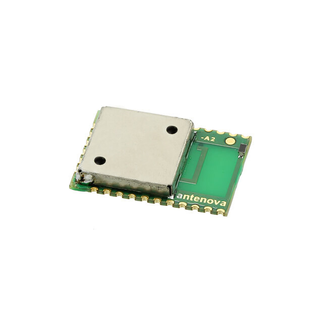
| 产品图片 |
|
| 产品型号 | ATA8202C-PXQW |
| rohs | 无铅 / 符合限制有害物质指令(RoHS)规范要求 |
| 产品系列 | - |
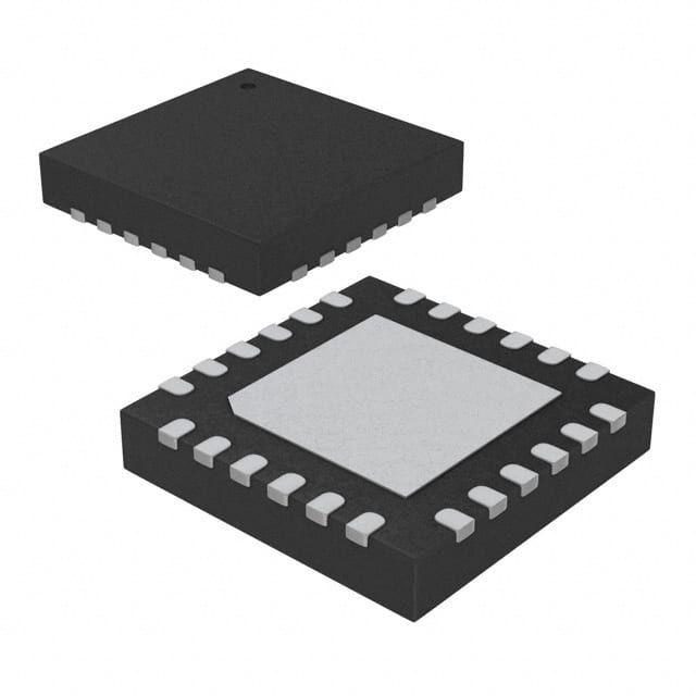
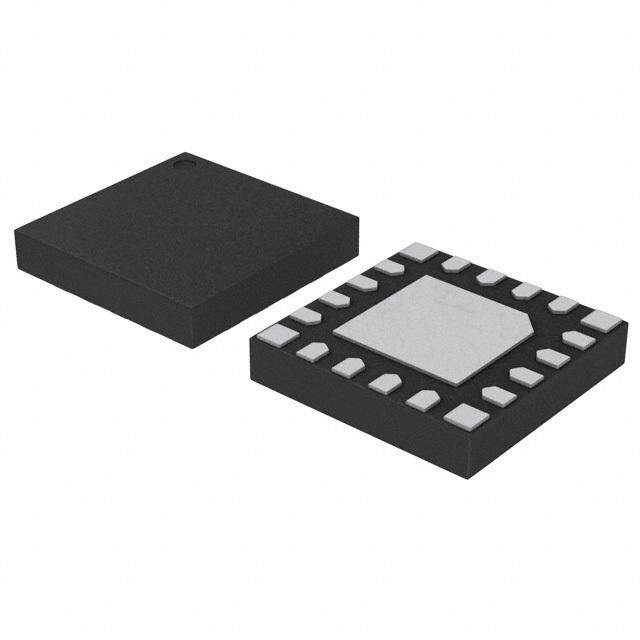
| 供应商器件封装 | 24-QFN(5x5) |
| 其它名称 | ATA8202C-PXQWCT |
| 包装 | 剪切带 (CT) |
| 天线连接器 | PCB,表面贴装 |
| 存储容量 | - |
| 封装/外壳 | 24-VQFN 裸露焊盘 |
| 工作温度 | -40°C ~ 85°C |
| 应用 | AMR,ISM,安防门禁 |
| 数据接口 | PCB,表面贴装 |
| 数据速率(最大值) | 20kbps |
| 标准包装 | 1 |
| 灵敏度 | -113dBm |
| 特性 | 配有 RSSI |
| 电压-电源 | 2.7 V ~ 3.3 V,4.5 V ~ 5.5 V |
| 电流-接收 | 6.7mA |
| 调制或协议 | ASK,FSK |
| 频率 | 433MHz |


_renders/CS4265-CNZR.jpg)


- 商务部:美国ITC正式对集成电路等产品启动337调查
- 曝三星4nm工艺存在良率问题 高通将骁龙8 Gen1或转产台积电
- 太阳诱电将投资9.5亿元在常州建新厂生产MLCC 预计2023年完工
- 英特尔发布欧洲新工厂建设计划 深化IDM 2.0 战略
- 台积电先进制程称霸业界 有大客户加持明年业绩稳了
- 达到5530亿美元!SIA预计今年全球半导体销售额将创下新高
- 英特尔拟将自动驾驶子公司Mobileye上市 估值或超500亿美元
- 三星加码芯片和SET,合并消费电子和移动部门,撤换高东真等 CEO
- 三星电子宣布重大人事变动 还合并消费电子和移动部门
- 海关总署:前11个月进口集成电路产品价值2.52万亿元 增长14.8%


PDF Datasheet 数据手册内容提取
ATA8201/ATA8202 UHF ASK/FSK Receiver DATASHEET Features ● Transparent RF receiver ICs for 315MHz (Atmel® ATA8201) and 433.92MHz (Atmel ATA8202) with high receiving sensitivity ● Fully integrated PLL with low phase noise VCO, PLL, and loop filter ● High FSK/ASK sensitivity: ● –105dBm (Atmel ATA8201, FSK, 9.6Kbits/s, Manchester, BER 10-3 ● –114dBm (Atmel ATA8201, ASK, 2.4Kbits/s, Manchester, BER 10-3) ● –104dBm (Atmel ATA8202, FSK, 9.6Kbits/s, Manchester, BER 10-3) ● –113dBm (Atmel ATA8202, ASK, 2.4Kbits/s, Manchester, BER 10-3) ● Supply current: 6.5mA in Active Mode (3V, 25°C, ASK Mode) ● Data rate: 1Kbit/s to 10Kbits/s Manchester ASK, 1Kbit/s to 20Kbits/s Manchester FSK with four programmable bit rate ranges ● Switching between modulation types ASK/FSK and different data rates possible in ≤1ms typically, without hardware modification on board to allow different modulation schemes ● Low standby current: 50µA at 3V, 25°C ● ASK/FSK receiver uses a low-IF architecture with high selectivity, blocking, and low intermodulation (typical 3-dB blocking 68.0dBCat±3MHz/74.0dBC at ±20.0MHz, system I1dBCP = –31dBm/system IIP3 = –24dBm) ● Telegram pause up to 52ms supported in ASK Mode ● Wide bandwidth AGC to handle large out-of-band blockers above the system I1dBCP ● 440-kHz IF frequency with 30-dB image rejection and 420-kHz IF bandwidth to support PLL transmitters with standard crystals or SAW-based transmitters ● RSSI (received signal strength indicator) with output signal dynamic range of 65dB ● Low in-band sensitivity change of typically ±2.0dB within ±160-kHz center frequency change in the complete temperature and supply voltage range ● Sophisticated threshold control and quasi-peak detector circuit in the data slicer ● Fast and stable XTO start-up circuit (> –1.4kΩ worst-case start impedance) ● Clock generation for microcontroller ● ESD protection at all pins (±4kV HBM, ±200V MM, ±500V FCDM) 4971G-INDCO-09/14
● Dual supply voltage range: 2.7V to 3.3V or 4.5V to 5.5V ● Temperature range: –40°C to +85°C ● Small 5mm×5mm QFN24 package Applications ● Industrial/aftermarket keyless entry and tire pressure monitoring systems ● Alarm, telemetering and energy metering systems ● Remote control systems for consumer and industrial markets ● Access control systems ● Home automation ● Home entertainment ● Toys Benefits ● Supports header and blanking periods of protocols common in RKE and TPM systems (up to 52ms in ASK Mode) λ ● All RF relevant functions are integrated. The single-ended RF input is suited for easy adaptation to /4 or printed-loop antennas ● Allows a low-cost application with only 8 passive components ● Optimal bandwidth maximizes sensitivity while maintaining SAW transmitter compatibility ● Clock output provides an external microcontroller crystal-precision time reference ● Well suited for use with Atmel® PLL transmitter ATA8401/ATA8402/ATA8403/ATA8404/ATA8405 2 ATA8201/ATA8202 [DATASHEET] 4971G–INDCO–09/14
1. General Description The Atmel® ATA8201/ATA8202 is a UHF ASK/FSK transparent receiver IC with low power consumption supplied in a small QFN24 package (body 5mm×5mm, pitch 0.65mm). Atmel ATA8202 is used in the 433MHz to 435MHz band of operation, and Atmel ATA8201 in 313MHz to 317MHz. For improved image rejection and selectivity, the IF frequency is fixed to 440kHz. The IF block uses an 8th-order band pass yielding a receive bandwidth of 420kHz. This enables the use of the receiver in both SAW- and PLL-based transmitter systems utilizing various types of data-bit encoding such as pulse width modulation, Manchester modulation, variable pulse modulation, pulse position modulation, and NRZ. Prevailing encryption protocols such as Keeloq® are easily supported due to the receiver’s ability to hold the current data slicer threshold for up to 52ms when incoming RF telegrams contain a blanking interval. This feature eliminates erroneous noise from appearing on the demodulated data output pin, and simplifies software decoding algorithms. The decoding of the data stream must be carried out by a connected microcontroller device. Because of the highly integrated design, the only required RF components are for the purpose of receiver antenna matching. Atmel ATA8201 and Atmel ATA8202 support Manchester bit rates of 1Kbit/s to 10Kbits/s in ASK and 1Kbit/s to 20Kbits/s in FSK mode. The four discrete bit rate passbands are selectable and cover 1.0Kbit/s to 2.5Kbits/s, 2.0Kbits/s to 5.0Kbits/s, 4.0Kbits/s to 10.0Kbits/s, and 8.0Kbits/s to 10.0Kbits/s or 20.0Kbits/s (for ASK or FSK, respectively). The receiver contains an RSSI output to provide an indication of received signal strength and a SENSE input to allow the customer to select a threshold below which the DATA signal is gated off. ASK/FSK and bit rate ranges are selected by the connected microcontroller device via pins ASK_NFSK, BR0, and BR1. Figure 1-1. System Block Diagram ATA8201/ATA8202 Digital Control Power Logic Supply Antenna RF Receiver Microcontroller (LNA, Mixer, 4 ... 8 VCO, PLL, Microcontroller IF Filter, Interface RSSI Amp., Demodulator) XTO ATA8201/ATA8202 [DATASHEET] 3 4971G–INDCO–09/14
Figure 1-2. Pinning QFN24 T K U S O F TA_ EM K_N 1 0 A D S R R X D C A B B R 24 23 22 21 20 19 TEST2 1 18 TEST3 TEST1 2 17 RSSI CLK_OUT 3 16 SENSE_CTRL CLK_OUT_CTRL1 4 15 SENSE CLK_OUT_CTRL0 5 14 LNA_IN ENABLE 6 13 LNA_GND 7 8 9 10 11 12 2 1 C V C D XTAL XTAL DVC VS5 _AVC GN V 3 S V Table 1-1. Pin Description Pin Symbol Function 1 TEST2 Test pin, during operation at GND 2 TEST1 Test pin, during operation at GND 3 CLK_OUT Output to clock a connected microcontroller 4 CLK_OUT_CTRL1 Input to control CLK_OUT (MSB) 5 CLK_OUT_CTRL0 Input to control CLK_OUT (LSB) 6 ENABLE Input to enable the XTO 7 XTAL2 Reference crystal 8 XTAL1 Reference crystal 9 DVCC Digital voltage supply blocking 10 VS5V Power supply input for voltage range 4.5V to 5.5V 11 VS3V_AVCC Power supply input for voltage range 2.7V to 3.3V 12 GND Ground 13 LNA_GND RF ground 14 LNA_IN RF input 15 SENSE Sensitivity control resistor Sensitivity selection 16 SENSE_CTRL Low: Normal sensitivity, High: Reduced sensitivity 17 RSSI Output of the RSSI amplifier 18 TEST3 Test pin, during operation at GND 19 RX Input to activate the receiver 20 BR0 Bit rate selection, LSB 21 BR1 Bit rate selection, MSB FSK/ASK selection 22 ASK_NFSK Low: FSK, High: ASK 23 CDEM Capacitor to adjust the lower cut-off frequency data filter 24 DATA_OUT Data output GND Ground/backplane (exposed die pad) 4 ATA8201/ATA8202 [DATASHEET] 4971G–INDCO–09/14
Figure 1-3. Block Diagram ASK/FSK ASK Power VS3V_AVCC CDEM Demo- Supply VS5V dulator FSK ASK/FSK ASK_NFSK Control IF Amp SENSE Data DATA_OUT Slicer SENSE_CTRL BR0 IF Filter BR1 GND Standby RX Logic Control LPF CLK_OUT_CTRL1 XTO DVCC CLK_OUT_CTRL0 Div. by 3, 6, 12 IF Amp CLK_OUT RSSI PLL LPF (/24, /32) XTO ENABLE TEST1 LNA_IN LNA VCO TEST2 LNA_GND TEST3 XTAL2 XTAL1 ATA8201/ATA8202 [DATASHEET] 5 4971G–INDCO–09/14
2. RF Receiver As seen in Figure 1-3 on page 5, the RF receiver consists of a low-noise amplifier (LNA), a local oscillator, and the signal processing part with mixer, IF filter, IF amplifier with analog RSSI, FSK/ASK demodulator, data filter, and data slicer. In receive mode, the LNA pre-amplifies the received signal which is converted down to a 440-kHz intermediate frequency (IF), then filtered and amplified before it is fed into an FSK/ASK demodulator, data filter, and data slicer. The received signal strength indicator (RSSI) signal is available at the pin RSSI. 2.1 Low-IF Receiver The receive path consists of a fully integrated low-IF receiver. It fulfills the sensitivity, blocking, selectivity, supply voltage, and supply current specification needed to design, e.g., an industrial/ aftermarket integrated receiver for RKE and TPM systems. A benefit of the integrated receive filter is that no external components needed. At 315MHz, the Atmel® ATA8201 receiver (433.92MHz for the Atmel ATA8202 receiver) has a typical system noise figure of 6.0dB (7.0dB), a system I1dBCP of –31dBm (–30dBm), and a system IIP3 of –24dBm (–23dBm). The signal path is linear for out-of-band disturbers up to the I1dBCP and hence there is no AGC or switching of the LNA needed, and a better blocking performance is achieved. This receiver uses an IF (intermediate frequency) of 440kHz, the typical image rejection is 30dB and the typical 3-dB IF filter bandwidth is 420kHz (f =440kHz±210kHz, f =230kHz and f =650kHz). The IF lo_IF hi_IF demodulator needs a signal-to-noise ratio of 8.5dB for 10Kbits/s Manchester with ±38kHz frequency deviation in FSK mode, thus, the resulting sensitivity at 315MHz (433.92MHz) is typically –105dBm (–104dBm). Due to the low phase noise and spurs of the synthesizer together with the 8th-order integrated IF filter, the receiver has a better selectivity and blocking performance than more complex double superhet receivers, without using external components and without numerous spurious receiving frequencies. A low-IF architecture is also less sensitive to second-order intermodulation (IIP2) than direct conversion receivers where every pulse or amplitude modulated signal (especially the signals from TDMA systems like GSM) demodulates to the receiving signal band at second-order non-linearities. 2.2 Input Matching at LNA_IN The measured input impedances as well as the values of a parallel equivalent circuit of these impedances can be seen in Table 2-1. The highest sensitivity is achieved with power matching of these impedances to the source impedance. Table 2-1. Measured Input Impedances of the LNA_IN Pin f [MHz] Z (RF_IN) [Ω ] R //C [pF] RF In In_p In_p 315 (72.4 – j298) 1300Ω //1.60 433.92 (55 – j216)Ω 900Ω //1.60 The matching of the LNA input to 50Ω is done using the circuit shown in Figure 2-1 and the values of the matching elements given in Table 2-2. The reflection coefficients were always ≤ –10dB. Note that value changes of C1 and L1 may be necessary to compensate individual board layout parasitics. The measured typical FSK and ASK Manchester-code sensitivities with a bit error rate (BER) of 10–3 are shown in Table 2-3 and Table 2-4 on page 7. These measurements were done with wire-wound inductors having quality factors reported in Table 2-2, resulting in estimated matching losses of 0.8dB at 315MHz and 433.92MHz. These losses can be estimated when calculating the parallel equivalent resistance of the inductor with R =2×π×f×L×Q and the matching loss with 10log(1+R /R ). loss L In_p loss Figure 2-1. Input Matching to 50 Ω ATA8201/ATA8202 RFIN C1 14 LNA_IN L1 6 ATA8201/ATA8202 [DATASHEET] 4971G–INDCO–09/14
Table 2-2. Input Matching to 50Ω f [MHz] C [pF] L [nH] Q RF 1 1 L1 315 2.2 68 20 433.92 2.2 36 15 Table 2-3. Measured Typical Sensitivity FSK, ±38kHz, Manchester, BER = 10–3 BR_Range_0 BR_Range_0 BR_Range_1 BR_Range_2 BR_Range_3 BR_Range_3 RF Frequency 1.0Kbit/s 2.5Kbits/s 5Kbits/s 10Kbits/s 10Kbits/s 20Kbits/s 315MHz –108dBm –108dBm –107dBm –105dBm –104dBm –104dBm 433.92MHz –107dBm –107dBm –106dBm –104dBm –103dBm –103dBm Table 2-4. Measured Typical Sensitivity 100% ASK, Manchester, BER = 10–3 BR_Range_0 BR_Range_0 BR_Range_1 BR_Range_2 BR_Range_3 RF Frequency 1.0Kbit/s 2.5Kbits/s 5Kbits/s 10Kbits/s 10Kbits/s 315MHz –114dBm –114dBm –113dBm –111dBm –109dBm 433.92MHz –113dBm –113dBm –112dBm –110dBm –108dBm Conditions for the sensitivity measurement: The given sensitivity values are valid for Manchester-modulated signals. For the sensitivity measurement the distance from edge to edge must be evaluated. As can be seen in Figure 6-1 on page 21, in a Manchester-modulated data stream, the time segments T and 2×T occur. EE EE To reach the specified sensitivity for the evaluation of T and 2×T in the data stream, the following limits should be used EE EE (T min, T max, 2×T min, 2×T max). EE EE EE EE Table 2-5. Limits for Sensitivity Measurements Bit Rate T Min T Typ T Max 2 × T Min 2 × T Typ 2 × T Max EE EE EE EE EE EE 1.0Kbit/s 260µs 500µs 790µs 800µs 1000µs 1340µs 2.4Kbits/s 110µs 208µs 310µs 320µs 416µs 525µs 5.0Kbits/s 55µs 100µs 155µs 160µs 200µs 260µs 9.6Kbits/s 27µs 52µs 78µs 81µs 104µs 131µs ATA8201/ATA8202 [DATASHEET] 7 4971G–INDCO–09/14
2.3 Sensitivity Versus Supply Voltage, Temperature and Frequency Offset To calculate the behavior of a transmission system, it is important to know the reduction of the sensitivity due to several influences. The most important are frequency offset due to crystal oscillator (XTO) and crystal frequency (XTAL) errors, temperature and supply voltage dependency of the noise figure, and IF-filter bandwidth of the receiver. Figure 2-2 and Figure 2-3 on page 8 show the typical sensitivity at 315MHz, ASK, 2.4Kbits/sand9.6Kbits/s, Manchester, Figure 2-4 and Figure 2-5 on page 9 show a typical sensitivity at 315MHz, FSK, 2.4Kbits/s and 9.6Kbits/s, ±38kHz, Manchester versus the frequency offset between transmitter and receiver at T =+25°C and supply voltage VS=VS3V_AVCC = VS5V = 3.0V. amb Figure 2-2. Measured Sensitivity (315MHz, ASK, 2.4Kbits/s, Manchester) Versus Frequency Offset Input Sensitivity (dBm) at BER < 1e-3, ATA8201, ASK, 2.4Kbits/s (Manchester), BR = 0 -118 -117 -116 m) -115 3.0V/25°C B -114 d sitivity ( ----111111113210 en -109 S -108 ut -107 p n -106 I -105 -104 -103 -300 -200 -100 0 100 200 300 delta RF (kHz) at 315MHz Figure 2-3. Measured Sensitivity (315MHz, ASK, 9.6Kbits/s, Manchester) Versus Frequency Offset Input Sensitivity (dBm) at BER < 1e-3, ATA8201, ASK, 9.6Kbits/s (Manchester), BR = 2 -115 -114 -113 m) -112 3.0V/25°C B -111 d sitivity ( ----111110000987 en -106 S -105 ut -104 p n -103 I -102 -101 -100 -300 -200 -100 0 100 200 300 delta RF (kHz) at 315MHz 8 ATA8201/ATA8202 [DATASHEET] 4971G–INDCO–09/14
Figure 2-4. Measured Sensitivity (315MHz, FSK, 2.4Kbits/s, ±38kHz, Manchester) Versus Frequency Offset Input Sensitivity (dBm) at BER < 1e-3, ATA8201, FSK, 2.4Kbits/s (Manchester), BR = 0 -112 -111 -110 m) -109 3.0V/25°C B -108 d y ( -107 vit -106 nsiti --110054 e S -103 ut -102 p -101 n I -100 -99 -98 -300 -200 -100 0 100 200 300 delta RF (kHz) at 315MHz Figure 2-5. Measured Sensitivity (315MHz, FSK, 9.6Kbits/s, ±38kHz, Manchester) Versus Frequency Offset Input Sensitivity (dBm) at BER < 1e-3, ATA8201, FSK, 9.64Kbits/s (Manchester), BR = 2 -110 -109 -108 m) -107 3.0V/25°C B -106 d y ( --110054 vit -103 siti -102 n -101 e S -100 ut -99 np -98 I -97 -96 -95 -300 -200 -100 0 100 200 300 delta RF (kHz) at 315MHz As can be seen in Figure 2-5 on page 9, the supply voltage has almost no influence. The temperature has an influence of about ±1.0dB, and a frequency offset of ±160kHz also influences by about ±1dB. All these influences, combined with the sensitivity of a typical IC (–105dB), are then within a range of –103.0dBm and –107.0dBm over temperature, supply voltage, and frequency offset. The integrated IF filter has an additional production tolerance of ±10kHz, hence, a frequency offset between the receiver and the transmitter of ±160kHz can be accepted for XTAL and XTO tolerances. Note: For the demodulator used in the Atmel® ATA8201/ATA8202, the tolerable frequency offset does not change with the data frequency. Hence, the value of ±160kHz is valid for 1Kbit/s to 10Kbits/s. This small sensitivity change over supply voltage, frequency offset, and temperature is very unusual in such a receiver. It is achieved by an internal, very fast, and automatic frequency correction in the FSK demodulator after the IF filter, which leads to a higher system margin. This frequency correction tracks the input frequency very quickly. If, however, the input frequency makes a larger step (for example, if the system changes between different communication partners), the receiver has to be → → restarted. This can be done by switching back to Standby mode and then again to Active mode (pin RX 1 0 1) or by → → generating a positive pulse on pin ASK_NFSK (0 1 0). ATA8201/ATA8202 [DATASHEET] 9 4971G–INDCO–09/14
2.4 RX Supply Current Versus Temperature and Supply Voltage Table 2-7 shows the typical supply current of the receiver in Active mode versus supply voltage and temperature with VS=VS3V_AVCC = VS5V. Table 2-6. Measured Current in Active Mode ASK VS = VS3V_AVCC = VS5V 3.0V T = 25°C 6.5mA amb Table 2-7. Measured Current in Active Mode FSK VS = VS3V_AVCC = VS5V 3.0V T = 25°C 6.7mA amb 2.5 Blocking, Selectivity As can be seen in Figure 2-6 on page 10, and Figure 2-7 and Figure 2-8 on page 11, the receiver can receive signals 3dB higher than the sensitivity level in the presence of large blockers of –34.5dBm or –28dBm with small frequency offsets of ±3MHz or ±20MHz. Figure 2-6, and Figure 2-7 on page 11 show the narrow-band blocking, and Figure 2-8 on page 11 shows the wide-band blocking characteristic. The measurements were done with a useful signal of 315MHz, FSK, 10Kbits/s, ±38kHz, Manchester, BR_Range2 with a level of –105dBm+3dB=–102dBm, which is 3dB above the sensitivity level. The figures show how much larger than –102dBm a continuous wave signal can be, until the BER is higher than 10–3. The measurements were done at the 50Ω input shown in Figure 2-1 on page 6. At 3 MHz, for example, the blocker can be 67.5dBC higher than – 102dBm, or –102dBm+67.5dBC=–34.5dBm. Figure 2-6. Close-in 3-dB Blocking Characteristic and Image Response at 315MHz 70 60 C) 50 B d el ( 40 v Le 30 g n 20 ki c o 10 Bl 0 -10 -2 -1.5 -1 -0.5 0 0.5 1 1.5 2 Distance from Interfering to Receiving Signal (MHz) 10 ATA8201/ATA8202 [DATASHEET] 4971G–INDCO–09/14
Figure 2-7. Narrow-band 3-dB Blocking Characteristic at 315MHz 80 70 C) 60 B d 50 vel ( 40 e L g 30 n ki 20 c o Bl 10 0 -10 -5 -4 -3 -2 -1 0 1 2 3 4 5 Distance from Interfering to Receiving Signal (MHz) Figure 2-8. Wide-band 3-dB Blocking Characteristic at 315MHz 80 70 C) 60 B d 50 vel ( 40 e L g 30 n ki 20 c o Bl 10 0 -10 -50 -40 -30 -20 -10 0 10 20 30 40 50 Distance from Interfering to Receiving Signal (MHz) Table 2-8 shows the blocking performance measured relative to –102dBm for some frequencies. Note that sometimes the blocking is measured relative to the sensitivity level 104dBm (denoted dBS), instead of the carrier –102dBm (denoted dBC). Table 2-8. Blocking 3dB Above Sensitivity Level With BER < 10–3 Frequency Offset Blocking Level Blocking +1.5MHz –44.5dBm 57.5dBC, 60.5dBS –1.5MHz –44.5dBm 57.5dBC, 60.5dBS +2MHz –39.0dBm 63dBC, 66dBS –2MHz –36.0dBm 66dBC, 69dBS +3MHz –34.5dBm 67.5dBC, 70.5dBS –3MHz –34.5dBm 67.5dBC, 70.5dBS +20MHz –28.0dBm 74dBC, 77dBS –20MHz –28.0dBm 74dBC, 77dBS The Atmel® ATA8201/ATA8202 can also receive FSK and ASK modulated signals if they are much higher than the I1dBCP. It can typically receive useful signals at –10dBm. This is often referred to as the nonlinear dynamic range (that is, the maximum to minimum receiving signal), and is 95dB for 10Kbits/s Manchester (FSK). This value is useful if the transmitter and receiver are very close to each other. ATA8201/ATA8202 [DATASHEET] 11 4971G–INDCO–09/14
2.6 In-band Disturbers, Data Filter, Quasi-peak Detector, Data Slicer If a disturbing signal falls into the received band, or if a blocker is not a continuous wave, the performance of a receiver strongly depends on the circuits after the IF filter. Hence, the demodulator, data filter, and data slicer are important. The data filter of the Atmel® ATA8201/ATA8202 functions also as a quasi-peak detector. This results in a good suppression of above mentioned disturbers and exhibits a good carrier-to-noise performance. The required useful-signal-to-disturbing- signal ratio, at a BER of 10–3, is less than 14dB in ASK mode and less than 3dB (BR_Range_0 to BR_Range_2) and 6dB (BR_Range_3) in FSK mode. Due to the many different possible waveforms, these numbers are measured for the signal, as well as for disturbers, with peak amplitude values. Note that these values are worst-case values and are valid for any type of modulation and modulating frequency of the disturbing signal, as well as for the receiving signal. For many combinations, lower carrier-to-disturbing-signal ratios are needed. 2.7 RSSI Output The output voltage of the pin RSSI is an analog voltage, proportional to the input power level. Using the RSSI output signal, the signal strength of different transmitters can be distinguished. The usable dynamic range of the RSSI amplifier is 65dB, the input power range P(RF ) is IN –110dBm to –45dBm, and the gain is 15mV/dB. Figure 2-9 shows the RSSI characteristic of a typical device at 315MHz with VS3V_AVCC=VS5V=3V and T =25°C with a matched input as shown in Table 2-2 and Figure 2-1 on page 6. At amb 433.92MHz, 1dB more signal level is needed for the same RSSI results. Figure 2-9. Typical RSSI Characteristic at 315MHz Versus Temperature and Supply Voltage 1.7 1.6 3V, 25°C 1.5 1.4 1.3 SI (V) 11..21 max: +9dBm S R 1.0 _ 0.9 V 0.8 min: -9dBm 0.7 0.6 0.5 0.4 -130 -120-110 -100 -90 -80 -70 -60 -50 -40 -30 -20 -10 Pin (dBm) As can be seen in Figure 2-9 on page 12, for single devices there is a variance over temperature and supply voltage range of ±3dB. The total variance over production, temperature, and supply voltage range is ±9dB. 2.8 Frequency Synthesizer The LO generates the carrier frequency for the mixer via a PLL synthesizer. The XTO (crystal oscillator) generates the reference frequency f . The VCO (voltage-controlled oscillator) generates the drive voltage frequency f for the mixer. f XTO LO LO is divided by the factor 24 (Atmel ATA8201) or 32 (Atmel ATA8202). The divided frequency is compared to f by the phase XTO frequency detector. The current output of the phase frequency detector is connected to the fully integrated loop filter, and thereby generates the control voltage for the VCO. By means of that configuration, the VCO is controlled in a way, such that f /24 (f /32) is equal to f . If f is determined, f can be calculated using the following formula: f =f /24 LO LO XTO LO XTO XTO LO (f =f /32). The synthesizer has a phase noise of –130dBC/Hz at 3MHz and spurs of –75dBC. XTO LO Care must be taken with the harmonics of the CLK output signal, as well as with the harmonics produced by a microprocessor clocked using the signal, as these harmonics can disturb the reception of signals. 12 ATA8201/ATA8202 [DATASHEET] 4971G–INDCO–09/14
3. XTO The XTO is an amplitude-regulated Pierce oscillator type with external load capacitances (2×16pF). Due to additional internal and board parasitics (C ) of approximately 2pF on each side, the load capacitance amounts to 2×18pF (9pF total). P The XTO oscillation frequency f is the reference frequency for the integer-N synthesizer. When designing the system in XTO terms of receiving and transmitting frequency offset, the accuracy of the crystal and XTO have to be considered. The XTO’s additional pulling (including the R tolerance) is only ±5ppm. The XTAL versus temperature, aging, and M tolerances is then the main source of frequency error in the local oscillator. The XTO frequency depends on XTAL properties and the load capacitances C at pin XTAL1 and XTAL2. The pulling (p) L1,2 of f from the nominal f is calculated using the following formula: XTO XTAL C C –C p = -----m--×------------------------L---N-------------L---------------------×10-6ppm 2 (C +C )×(C +C ) O LN O L C , the crystal’s motional capacitance; C , the shunt capacitance; and C , the nominal load capacitance of the XTAL, are m 0 LN found in the datasheet. C is the total actual load capacitance of the crystal in the circuit, and consists of C and C L L1 L2 connected in series. Figure 3-1. Crystal Equivalent Circuit Crystal Equivalent Circuit XTAL C0 Lm Cm Rm C C L1 L2 C = C x C / (C + C ) L L1 L2 L1 L2 With C ≤ 10fF, C ≥1.0pF, C =9pF and C =16pF±1%, the pulling amounts to P≤ ±1ppm. m 0 LN L1,2 The C of the XTAL has to be lower than C /2 =7.9pF for a Pierce oscillator type in order to not enter the steep region of 0 Lmin pulling versus load capacitance where there is risk of an unstable oscillation. To ensure proper start-up behavior, the small signal gain and the negative resistance provided by this XTO at start is very large. For example, oscillation starts up even in the worst case with a crystal series resistance of 1.5kΩ at C ≤ 2.2pF with 0 this XTO. The negative resistance is approximately given by ⎧Z ×Z +Z ×Z +Z ×Z ×gm⎫ Re{Zxtocore} = Re⎨----1---Z-------+---3--Z--------+---2--Z--------+--3---Z-------×---1--Z--------×--3---g---m----------⎬ ⎩ 1 2 3 1 2 ⎭ with Z and Z as complex impedances at pins XTAL1 and XTAL2, hence 1 2 Z =–j/(2×p×f ×C )+5Ω and Z =–j/(2×p×f ×C )+5Ω . 1 XTO L1 2 XTO L2 Z consists of crystal C in parallel with an internal 110-kΩ resistor, hence 3 0 Z =–j/(2×p×f ×C )/110kΩ , gm is the internal transconductance between XTAL1 and XTAL2, with typically 20mS at 3 XTO 0 25°C. With f =13.5MHz, gm=20mS, C =9pF, and C =2.2pF, this results in a negative resistance of about 2kΩ . The worst XTO L 0 case for technology, supply voltage, and temperature variations is then always higher than 1.4kΩ for C ≤ 2.2pF. 0 Due to the large gain at start, the XTO is able to meet a very low start-up time. The oscillation start-up time can be estimated with the time constant τ. 2 τ = ------------------------------------------------------------------------------------------------------------ 4×π2×f 2×C ×(Re(Z )+R ) XTAL m xtocore m ATA8201/ATA8202 [DATASHEET] 13 4971G–INDCO–09/14
After 10τ to 20τ, an amplitude detector detects the oscillation amplitude and sets XTO_OK to High if the amplitude is large enough; this activates the CLK_OUT output if it is enabled via the pins CLK_OUT_CTRL0 and CLK_OUT_CTRL1. Note that the necessary conditions of the DVCC voltage also have to be fulfilled. It is recommended to use a crystal with C =3.0fF to 10fF, C =9pF, R <120Ω and C =1.0pF to 2.2pF. m LN m 0 Lower values of C can be used, slightly increasing the start-up time. Lower values of C or higher values of C (up to 15fF) m 0 m can also be used, with only little influence on pulling. Figure 3-2. XTO Block Diagram CL1 CL2 XTAL1 XTAL2 CLK_OUT_CTRL0 CLK_OUT_CTRL1 CLK_OUT & fFXTO Divider /3, /6, /12 XTO_OK Amplitude Detector Divider /16 fDCLK The relationship between f and the f is shown in Table 3-1. XTO RF Table 3-1. Calculation of f RF Frequency [MHz] f [MHz] f XTO RF 433.92 (Atmel ATA8202) 13.57375 f × 32 – 440kHz XTO 315.0 (Atmel ATA8201) 13.1433 f × 24 – 440kHz XTO Attention must be paid to the harmonics of the CLK_OUT output signal f as well as to the harmonics produced by an CLK_OUT microprocessor clocked with it, since these harmonics can disturb the reception of signals if they get to the RF input. If the CLK_OUT signal is used, it must be carefully laid out on the application PCB. The supply voltage of the microcontroller must also be carefully blocked. 14 ATA8201/ATA8202 [DATASHEET] 4971G–INDCO–09/14
3.1 Pin CLK_OUT Pin CLK_OUT is an output to clock a connected microcontroller. The clock is available in Standby and Active modes. The frequency f can be adjusted via the pins CLK_OUT_CTRL0 and CLK_OUT_CTRL1, and is calculated as follows: CLK_OUT Table 3-2. Setting of f CLK_OUT CLK_OUT_CTRL1 CLK_OUT_CTRL0 Function Clock on pin CLK_OUT is switched off 0 0 (Low level on pin CLK_OUT) 0 1 f =f /3 CLK_OUT XTO 1 0 f =f /6 CLK_OUT XTO 1 1 f =f /12 CLK_OUT XTO The signal at CLK_OUT output has a nominal 50% duty cycle. To save current, it is recommended that CLK_OUT be switched off during Standby mode. 3.2 Basic Clock Cycle of the Digital Circuitry The complete timing of the digital circuitry is derived from one clock. As seen in Figure 3-2 on page 14, this clock cycle, T , is derived from the crystal oscillator (XTO) in combination with a divider. DCLK f f = ---X---T---O-- DCLK 16 T controls the following application relevant parameters: DCLK - Debouncing of the data signal stream - Start-up time of the RX signal path The start-up time and the debounce characteristic depend on the selected bit rate range (BR_Range) which is defined by pins BR0 and BR1. The clock cycle T is defined by the following formulas for further reference: XDCLK BR_Range ⇒ BR_Range0: T = 8 × T XDCLK DCLK BR_Range1: T = 4 × T XDCLK DCLK BR_Range2: T = 2 × T XDCLK DCLK BR_Range3: T = 1 × T XDCLK DCLK ATA8201/ATA8202 [DATASHEET] 15 4971G–INDCO–09/14
4. Sensitivity Reduction The output voltage of the RSSI amplifier is internally compared to a threshold voltage V . V is determined by the Th_red Th_red value of the external resistor R . R is connected between the pins SENSE and VS3V_AVCC (see Figure 10-1 on Sense Sense page 25). The output of the comparator is fed into the digital control logic. By this means, it is possible to operate the receiver at a lower sensitivity. If the level on input pin SENSE_CTRL is low, the receiver operates at full sensitivity. If the level on input pin SENSE_CTRL is high, the receiver operates at a lower sensitivity. The reduced sensitivity is defined by the value of R , the maximum sensitivity by the signal-to-noise ratio of the LNA input. The reduced sensitivity depends Sense on the signal strength at the output of the RSSI amplifier. Since different RF input networks may exhibit slightly different values for the LNA gain, the sensitivity values given in the electrical characteristics refer to a specific input matching. This matching is illustrated in Figure 2-1 on page 6 and exhibits the best possible sensitivity. If the sensitivity reduction feature is not used, pin SENSE can be left open, pin SENSE_CTRL must be set to GND. To operate with reduced sensitivity, pin SENSE_CTRL must be set to high before the RX signal path will be enabled by setting pin RX to high (see Figure 4-1 on page 16). As long as the RSSI level is lower than V (defined by the external Th_red resistor R ) no data stream is available on pin DATA_OUT (low level on pin DATA_OUT). An internal RS flip-flop will be Sense set to high the first time the RSSI voltage crosses V , and from then on the data stream will be available on pin Th_red DATA_OUT. From then on the receiver also works with full sensitivity. This makes sure that a telegram will not be interrupted if the RSSI level varies during the transmission. The RS flip-flop can be set back, and thus the receiver switched back to reduced sensitivity, by generating a positive pulse on pin ASK_NFSK (see Figure 4-2 on page 17). In FSK mode, operating with reduced sensitivity follows the same way. Figure 4-1. Reduced Sensitivity Active ENABLE ASK_NFSK SENSE_CTRL RX VTh_red RSSI tStartup_PLL tStartup_Sig_Proc DATA_OUT 16 ATA8201/ATA8202 [DATASHEET] 4971G–INDCO–09/14
Figure 4-2. Restart Reduced Sensitivity ENABLE ASK_NFSK SENSE_CTRL RX VTh_red RSSI tStartup_Sig_Proc DATA_OUT 5. Power Supply Figure 5-1. Power Supply VS3V_AVCC SW_DVCC IN V_REG OUT VS5V DVCC 3.0V typ. EN RX The supply voltage range of the Atmel® ATA8201/ATA8202 is 2.7V to 3.3V or 4.5V to 5.5V. Pin VS3V_AVCC is the supply voltage input for the range 2.7V to 3.3V, and is used in battery applications using a single lithium 3V cell. Pin VS5V is the voltage input for the range 4.5V to 5.5V (car applications) in this case the voltage regulator V_REG regulates VS3V_AVCC to typically 3.0V. If the voltage regulator is active, a blocking capacitor of 2.2µF has to be connected to VS3V_AVCC (see Figure 10-1 on page 25). DVCC is the internal operating voltage of the digital control logic and is fed via the switch SW_DVCC by VS3V_AVCC. DVCC must be blocked on pin DVCC with 68nF (see Figure 9-1 on page 24 and Figure 10-1 on page 25). Pin RX is the input to activate the RX signal processing and set the receiver to Active mode. ATA8201/ATA8202 [DATASHEET] 17 4971G–INDCO–09/14
5.1 OFF Mode A low level on pin RX and ENABLE will set the receiver to OFF mode (low power mode). In this mode, the crystal oscillator is shut down and no clock is available on pin CLK_OUT. The receiver is not sensitive to a transmitter signal in this mode. Table 5-1. Standby Mode RX ENABLE Function 0 0 OFF mode 5.2 Standby Mode The receiver activates the Standby mode if pin ENABLE is set to “1”. In Standby mode, the XTO is running and the clock on pin CLK_OUT is available after the start-up time of the XTO has elapsed (dependent on pin CLK_OUT_CTRL0 and CLK_OUT_CTRL1). During Standby mode, the receiver is not sensitive to a transmitter signal. In Standby mode, the RX signal path is disabled and the power consumption I is typically 50µA (CLK_OUT output off, Standby VS3V_AVCC=VS5V=3V). The exact value of this current is strongly dependent on the application and the exact operation mode, therefore check the section “Electrical Characteristics: General” on page 26 for the appropriate application case. Table 5-2. Standby Mode RX ENABLE Function 0 1 Standby mode Figure 5-2. Standby Mode (CLK_OUT_CTRL0 or CLK_OUT_CTRL1 = 1) CLK_OUT tXTO_Startup ENABLE Standby Mode 5.3 Active Mode The Active mode is enabled by setting the level on pin RX to high. In Active mode, the RX signal path is enabled and if a valid signal is present it will be transferred to the connected microcontroller. Table 5-3. Active Mode RX ENABLE Function 1 1 Active mode During T the PLL is enabled and starts up. If the PLL is locked, the signal processing circuit starts up Startup_PLL (T ). After the start-up time, all circuits are in stable condition and ready to receive. The duration of the start-up Startup_Sig_Proc sequence depends on the selected bit rate range. 18 ATA8201/ATA8202 [DATASHEET] 4971G–INDCO–09/14
Figure 5-3. Active Mode CLK_OUT ENABLE RX DATA_OUT DATA_OUT valid tStartup_PLL tStartup_Sig_Proc IStandby IStartup_PLL IActive IActive Standby Mode Startup Active Mode Table 5-4. Start-up Time Atmel ATA8202 (433.92MHz) Atmel ATA8201 (315MHz) BR1 BR0 T T T T Startup_PLL Startup_Sig_Proc Startup_PLL Startup_Sig_Proc 0 0 1096µs 1132µs 0 1 644µs 665µs 261µs 269µs 1 0 417µs 431µs 1 1 304µs 324µs Table 5-5. Modulation Scheme ASK_NFSK RF at Pin LNA_IN Level at Pin DATA_OUT IN f 1 FSK_H 0 f 0 FSK_L f on 1 ASK 1 f off 0 ASK ATA8201/ATA8202 [DATASHEET] 19 4971G–INDCO–09/14
6. Bit Rate Ranges Configuration of the bit rate ranges is carried out via the two pins BR0 and BR1. The microcontroller uses these two interface lines to set the corner frequencies of the band-pass data filter. Switching the bit rate ranges while the RF front end is in Active mode can be done on the fly and will not take longer than 100µs if done while remaining in either ASK or FSK mode. If the modulation scheme is changed at the same time, the switching time is (T , see Figure 7-1 on page 22). Startup_Sig_Proc Each BR_Range is defined by a minimum edge-to-edge time. To maintain full sensitivity of the receiver, edge-to-edge transition times of incoming data should not be less than the minimum for the selected BR_Range. Table 6-1. BR Ranges ASK Minimum Edge-to-edge Edge-to-edge Time Period T EE Recommended Bit Rate Time Period T of the of the Data Signal During the EE BR1 BR0 BR_Range (Manchester)(1) Data Signal(2) Start-up Period(3) 0 0 BR_Range0 1.0Kbit/s to 2.5Kbits/s 200µs 200µs to 500µs 0 1 BR_Range1 2.0Kbits/s to 5.0Kbits/s 100µs 100µs to 250µs 1 0 BR_Range2 4.0Kbits/s to 10.0Kbits/s 50µs 50µs to 125µs 1 1 BR_Range3 8.0Kbits/s to 10.0Kbits/s 50µs 50µs to 62.5µs Table 6-2. BR Ranges FSK Minimum Edge-to-edge Edge-to-edge Time Period T EE Recommended Bit Rate Time Period T of the of the Data Signal During the EE BR1 BR0 BR_Range (Manchester)(1) Data Signal(2) Start-up Period(3) 0 0 BR_Range0 1.0Kbit/s to 2.5Kbits/s 200µs 200µs to 500µs 0 1 BR_Range1 2.0Kbits/s to 5.0Kbits/s 100µs 100µs to 250µs 1 0 BR_Range2 4.0Kbits/s to 10.0Kbits/s 50µs 50µs to 125µs 1 1 BR_Range3 8.0Kbits/s to 20.0Kbits/s 25µs 25µs to 62.5µs Note: If during the start-up period (T +T ) there is no RF signal, the data filter settles to the Startup_PLL Startup_Sig_Proc noise floor, leading to noise on pin DATA_OUT. Notes: 1. As can be seen, a bit stream of, for example, 2.5Kbits/s can be received in BR_Range0 and BR_Range1 (overlapping BR_Ranges). To get the full sensitivity, always use the lowest possible BR_Range (here, BR_Range0). The advantage in the next higher BR_Range (BR_Range1) is the shorter start-up period, mean- ing lower current consumption during Polling mode. Thus, it is a decision between sensitivity and current consumption. 2. The receiver is also capable of receiving non-Manchester-modulated signals, such as PWM, PPM, VPWM, NRZ. In ASK mode, the header and blanking periods occurring in Keeloq-like protocols (up to 52ms) are supported. 3. To ensure an accurate settling of the data filter during the start-up period (T +T ), the Startup_PLL Startup_Sig_Proc edge-to-edge time T of the data signal (preamble) must be inside the given limits during this period. EE 20 ATA8201/ATA8202 [DATASHEET] 4971G–INDCO–09/14
Figure 6-1. Examples of Supported Modulation Formats TEE TEE TEE TEE MAN: Logic 0 Logic 1 TEE TEE TEE TEE TEE TEE PWM: Logic 0 Logic 1 Logic 0 Logic 1 TEE TEE TEE VPWM: On Transition Low to High Logic 0 Logic 1 TEE TEE TEE On Transition High to Low TEE TEE TEE TEE TEE TEE PPM: Logic 0 Logic 1 TEE TEE NRZ: Logic 0 Logic 1 Figure 6-2. Supported Header and Blanking Periods Preamble Header Data Burst Guard Time Data Burst ATA8201/ATA8202 [DATASHEET] 21 4971G–INDCO–09/14
7. ASK_NFSK The ASK_NFSK pin allows the microcontroller to rapidly switch the RF front end between demodulation modes. A logic 1 on this pin selects ASK mode, and a logic 0 FSK mode. The time to change modes (T ) depends on the bit rate Startup_Sig_Proc range being selected (not current bit rate range) and is given in Table 5-4 on page 19. This response time is specified for applications that require an ASK preamble followed by FSK data (for typical TPM applications). During T , the Startup_Sig_Proc level on pin DATA_OUT is low. Figure 7-1. ASK Preamble 2.4Kbits/s followed by FSK Data 9.6Kbits/s ENABLE RX BR1 BR0 ASK_NFSK DATA_OUT Data valid BR0 Data valid BR3 TStartup_Sig_Proc 22 ATA8201/ATA8202 [DATASHEET] 4971G–INDCO–09/14
8. Polling Current Calculation Figure 8-1. Polling Cycle ENABLE RX L L L L P P up_ IActive up_ IActive art art St St I I ISupply IStandby IStandby TBitcheck (= 1 / Signal_Bitrate (average) TStartup_Sig_Proc (Startup Signal Processing) TStartup_PLL (Startup RF-PLL) In an industrial or aftermarket RKE and TPM system, the average chip current in Polling mode, I , is an important Polling parameter. The polling period must be controlled by the connected microcontroller via the pins ENABLE and RX. The polling current can be calculated as follows: I =(T /T )×I +(T /T )×I + Polling Startup_PLL Polling_Period Startup_PLL Startup_Sig_Proc Polling_Period Active (T /T )×I +(T –T –T –T )/ T ×I Bitcheck Polling_Period Active Polling_Period Startup_PLL Startup_Sig_Proc Bitcheck Polling_Period Standby T : depends on 315MHz/433.92MHz application. Startup_PLL T : depends on 315MHz/433.92MHz application and the selected bit Startup_Sig_Proc rate range. T : depends on the signal bit rate (1/Signal_Bit_Rate). Bitcheck T : depends on the transmitter telegram (preburst). Polling_Period I : depends on 3V or 5V application and the setting of pin CLK_OUT. Startup_PLL I : depends on 3V or 5V application, ASK or FSK mode and the setting of Active pin CLK_OUT. I : depends on 3V or 5V application and the setting of pin CLK_OUT. Standby Example:- 315-MHz application (ATA8201), bit rate: 9.6Kbits/s, T =8ms Polling_Period --> T = 269µs Startup_PLL --> T = 324µs (Bit Rate Range 3) Startup_Sig_Proc --> T = 104µs Bitcheck 3V application; ASK mode, CLK_OUT disabled --> I = 4.5mA Startup_PLL --> I = 6.5mA Active --> I = 0.05mA Standby --> I = 0.545mA Polling ATA8201/ATA8202 [DATASHEET] 23 4971G–INDCO–09/14
9. 3V Application Figure 9-1. 3V Application 15nF T M K 1 0 X output TEST2A_OU CDE _NFS BR BR RTEST3 T K A S D A output TEST1 RSSI r e oll ATA8201/ r output CLK_OUT SENSE_CTRL nt ATA8202 o c o output CLK_OUT_CTRL1 SENSE r Mic 2.2pF RFIN input CLK_OUT_CTRL0 LNA_IN C C VSS oVuCtpCut ENABXTAL2LE XTAL1 DVCC VS5V VS3V_AV LNAGND_GND 6381n5HM/H3z6/n4H33.92MHz 68nF 18pF 18pF 68nF VCC = 2.7V to 3.3V Note: Paddle (backplane) must be connected to GND 24 ATA8201/ATA8202 [DATASHEET] 4971G–INDCO–09/14
10. 5V Application Figure 10-1. 5V Application with Reduced/Full Sensitivity 15nF output T M K 1 0 X output TEST2A_OU CDE _NFS BR BR RTEST3 T K A S D A er output TEST1 RSSI oll ntr output CLK_OUT ATA8201/ SENSE_CTRL o ATA8202 oc RSense cr output CLK_OUT_CTRL1 SENSE Mi 2.2pF input CLK_OUT_CTRL0 LNA_IN C VSS oVuCtpCut ENABXTAL2LE XTAL1 DVCC VS5V VS3V_AVC LNAGND_GND RFIN 68nH/36nH 315MHz/433.92MHz 68nF 18pF 18pF 2.2µF 68nF VCC = 4.5V to 5.5V Note: Paddle (backplane) must be connected to GND ATA8201/ATA8202 [DATASHEET] 25 4971G–INDCO–09/14
11. Absolute Maximum Ratings Stresses beyond those listed under “Absolute Maximum Ratings” may cause permanent damage to the device. This is a stress rating only and functional operation of the device at these or any other conditions beyond those indicated in the operational sections of this specification is not implied. Exposure to absolute maximum rating conditions for extended periods may affect device reliability. Parameters Symbol Min. Max. Unit Junction temperature T +150 °C j Storage temperature T –55 +125 °C stg Ambient temperature T –40 +85 °C amb Supply voltage VS5V V +6 V S ESD (Human Body Model ESD S 5.1) HBM –4 +4 kV every pin ESD (Machine Model JEDEC A115A) MM –200 +200 V every pin ESD (Field Induced Charge Device Model ESD FCDM –500 +500 V STM 5.3.1-1999) every pin Maximum input level, input matched to 50Ω P 0 dBm in_max 12. Thermal Resistance Parameters Symbol Value Unit Junction ambient R 35 K/W thJA 13. Electrical Characteristics: General All parameters refer to GND and are valid for T =25°C, V =V =3V, and V =5V. Typical values are given at amb VS3V_AVCC VS5V VS5V f =315MHz unless otherwise specified. Details about current consumption, timing, and digital pin properties can be found in the RF specific sections of the “Electrical Characteristics”. No. Parameters Test Conditions Pin(1) Symbol Min. Typ. Max. Unit Type* 1 OFF Mode V =V ≤3V 10, 11 4 µA A Supply current in OFF VS3V_AVCC VS5V 1.1 V =5V 10 I 4 µA A mode VS5V SOFF CLK_OUT disabled 2 Standby Mode XTO running V =V ≤3V 10,11 I 50 100 µA A VS3V_AVCC VS5V Standby Supply current CLK_OUT disabled 2.1 Standby mode XTO running V =5V 10,11 I 50 100 µA A VS5V Standby CLK_OUT disabled XTO startup 2.2 System start-up time XTAL: C =5fF, T 0.3 ms A m XTO_Startup C =1.8pF, R =15Ω 0 m *) Type means: A = 100% tested, B = 100% correlation tested, C = Characterized on samples, D = Design parameter Note: 1. Pin numbers in parenthesis were measured with RF_IN matched to 50 Ω according to Figure 2-1 on page 6 with compo- nent values as in Table 2-2 on page 7 (RF ). IN 26 ATA8201/ATA8202 [DATASHEET] 4971G–INDCO–09/14
13. Electrical Characteristics: General (Continued) All parameters refer to GND and are valid for T =25°C, V =V =3V, and V =5V. Typical values are given at amb VS3V_AVCC VS5V VS5V f =315MHz unless otherwise specified. Details about current consumption, timing, and digital pin properties can be found in the RF specific sections of the “Electrical Characteristics”. No. Parameters Test Conditions Pin(1) Symbol Min. Typ. Max. Unit Type* From Standby mode to Active mode T + Active mode start-up Startup_PLL 2.3 BR_Range_3 T A time Startup_Sig_Pro Atmel ATA5745 565 µs c Atmel ATA5746 593 µs 3 Active Mode RF operating frequency Atmel ATA8201 14 fRF 313 317 MHz A 3.1 range Atmel ATA8202 14 f 433 435 MHz A RF V =V =3V VS3V_AVCC VS5V ASK mode 10,11 I 6.5 mA A CLK_OUT disabled Active SENSE_CTRL = 0 V =V =3V VS3V_AVCC VS5V FSK mode 10,11 I 6.7 mA A CLK_OUT disabled Active Supply current Active SENSE_CTRL = 0 3.2 mode V =5V VS5V ASK mode 10 I 6.7 mA A CLK_OUT disabled Active SENSE_CTRL = 0 V =5V VS5V FSK mode 10 I 6.9 mA A CLK_OUT disabled Active SENSE_CTRL = 0 V =V =3V VS3V_AVCC VS5V T = 8ms Polling_Period Supply current Polling BR_Range_3, ASK 3.3 10,11 I 545 µA C mode mode, CLK_OUT Polling disabled Data rate = 9.6Kbits/s FSK deviation f = ±38kHz DEV BER = 10–3 T = 25°C amb Bit rate 9.6Kbits/s BR2 (14) P –103 –105 –106.5 dBm B Input sensitivity FSK REF_FSK 3.4 fRF = 315MHz Bit rate 2.4Kbits/s BR0 (14) PREF_FSK –106 –108 –109.5 dBm B FSK deviation ±18kHz to ±50kHz Bit rate 9.6Kbits/s BR2 (14) P –101 dBm B REF_FSK Bit rate 2.4Kbits/s BR0 (14) P –104 dBm B REF_FSK *) Type means: A = 100% tested, B = 100% correlation tested, C = Characterized on samples, D = Design parameter Note: 1. Pin numbers in parenthesis were measured with RF_IN matched to 50 Ω according to Figure 2-1 on page 6 with compo- nent values as in Table 2-2 on page 7 (RF ). IN ATA8201/ATA8202 [DATASHEET] 27 4971G–INDCO–09/14
13. Electrical Characteristics: General (Continued) All parameters refer to GND and are valid for T =25°C, V =V =3V, and V =5V. Typical values are given at amb VS3V_AVCC VS5V VS5V f =315MHz unless otherwise specified. Details about current consumption, timing, and digital pin properties can be found in the RF specific sections of the “Electrical Characteristics”. No. Parameters Test Conditions Pin(1) Symbol Min. Typ. Max. Unit Type* ASK 100% level of carrier, BER = 10–3 Input sensitivity ASK T = 25°C 3.5 amb f = 315MHz RF Bit rate 9.6Kbits/s BR2 (14) P –109 –111 –112.5 dBm B REF_ASK Bit rate 2.4Kbits/s BR0 (14) P –112 –114 –115.5 dBm B REF_ASK Sensitivity change at f =315MHz to RF f =433.92MHz f =433.92MHz 3.6 RF RF (14) Δ P +1 dB B compared to P=P + Δ P REF1 REF_ASK REF1 f =315MHz P=P + Δ P RF REF_FSK REF1 FSK f = ±38kHz DEV Δ f ≤ ±160kHz OFFSET Sensitivity change ASK 100% versus temperature, Δ f ≤ ±160kHz 3.7 OFFSET (14) Δ P +4.5 –1.5 B supply voltage and P = P + Δ P + REF2 REF_ASK REF1 frequency offset Δ P REF2 P = P + Δ P + REF_FSK REF1 Δ P REF2 R connected from dBm Sense pin SENSE to P (peak Ref_Red pin VS3V_AVCC level) R = 62kΩ Sense –76 dBm C f = 433.92MHz in Reduced sensitivity R = 82kΩ Sense –88 dBm C f = 433.92MHz in 3.8 R = 62kΩ Sense –76 dBm C f = 315MHz in R = 82kΩ Sense –88 dBm C f = 315MHz in Reduced sensitivity R = 62kΩ Sense variation over full R = 82kΩ Δ P –10 +10 dB Sense Red operating range P = P + P Red Ref_Red Δ Red Maximum frequency difference of f between RF receiver and transmitter Maximum frequency in FSK mode (f is the 3.9 RF (14) Δ f –160 +160 kHz B offset in FSK mode center frequency of the OFFSET FSK signal with f = 10Kbits/s BIT f = ±38kHz DEV *) Type means: A = 100% tested, B = 100% correlation tested, C = Characterized on samples, D = Design parameter Note: 1. Pin numbers in parenthesis were measured with RF_IN matched to 50 Ω according to Figure 2-1 on page 6 with compo- nent values as in Table 2-2 on page 7 (RF ). IN 28 ATA8201/ATA8202 [DATASHEET] 4971G–INDCO–09/14
13. Electrical Characteristics: General (Continued) All parameters refer to GND and are valid for T =25°C, V =V =3V, and V =5V. Typical values are given at amb VS3V_AVCC VS5V VS5V f =315MHz unless otherwise specified. Details about current consumption, timing, and digital pin properties can be found in the RF specific sections of the “Electrical Characteristics”. No. Parameters Test Conditions Pin(1) Symbol Min. Typ. Max. Unit Type* With up to 2dB loss of sensitivity. Note that the tolerable Supported FSK frequency offset is 12kHz 3.10 (14) f ±18 ±38 ±50 kHz B frequency deviation lower for f = ±50kHz DEV DEV than for f = ±38kHz, DEV hence, Δ f ≤ ±148kHz OFFSET f = 315MHz (14) NF 6.0 9 dB B RF 3.11 System noise figure f = 433.92MHz (14) NF 7.0 10 dB B RF f = 433.92MHz f 440 kHz A RF IF 3.12 Intermediate frequency f = 315MHz f 440 kHz A RF IF 3dB bandwidth This value is for information only! 3.13 System bandwidth Note that for crystal and (14) SBW 435 kHz A system frequency offset calculations, Δ f OFFSET must be used. Δ f = 1.8MHz meas1 System out-band Δ f = 3.6MHz (14) IIP3 –24 dBm C meas2 3.14 3rd-order input intercept f = 315MHz RF point f = 433.92MHz (14) IIP3 –23 dBm C RF Δ f = 1MHz System outband input 1- meas1 (14) I1dBCP –31 –36 dBm C 3.15 fRF = 315MHz dB compression point f = 433.92MHz (14) I1dBCP –30 –35 dBm C RF f = 315MHz 14 Z (72.4 – j298) Ω C RF in_LNA 3.16 LNA input impedance f = 433.92MHz 14 Z (55 – j216) Ω C RF in_LNA Maximum peak RF input BER < 10–3, ASK: 100% (14) PIN_max +5 –10 dBm C 3.17 level, ASK and FSK FSK: f = ±38kHz (14) P +5 –10 dBm C DEV IN_max f < 1GHz (14) –57 dBm C f >1GHz (14) –47 dBm C f = 315.44MHz –90 LO 2 × f (14) –94 dBm C 3.18 LO spurs at LNA_IN LO 4 × f –68 LO f = 434.36MHz –92 LO 2 × f (14) –88 dBm C LO 4 × f –58 LO With the complete image band A 3.19 Image rejection f = 315MHz (14) 24 30 dB RF f = 433.92MHz (14) 24 30 dB A RF *) Type means: A = 100% tested, B = 100% correlation tested, C = Characterized on samples, D = Design parameter Note: 1. Pin numbers in parenthesis were measured with RF_IN matched to 50 Ω according to Figure 2-1 on page 6 with compo- nent values as in Table 2-2 on page 7 (RF ). IN ATA8201/ATA8202 [DATASHEET] 29 4971G–INDCO–09/14
13. Electrical Characteristics: General (Continued) All parameters refer to GND and are valid for T =25°C, V =V =3V, and V =5V. Typical values are given at amb VS3V_AVCC VS5V VS5V f =315MHz unless otherwise specified. Details about current consumption, timing, and digital pin properties can be found in the RF specific sections of the “Electrical Characteristics”. No. Parameters Test Conditions Pin(1) Symbol Min. Typ. Max. Unit Type* Peak level of useful signal to peak level of interferer for BER < 10–3 with any modulation Useful signal to interferer 3.20 scheme of interferer ratio FSK BR_Ranges 0, 1, 2 (14) SNR 2 3 dB B FSK0-2 FSK BR_Range_3 (14) SNR 4 6 dB B FSK3 ASK (P < P ) (14) SNR 10 14 dB B RF RFIN_High ASK Dynamic range (14),17 D 65 dB A RSSI Lower level of range f = 315MHz (14),17 P –110 dBm A RF RFIN_Low f = 433.92MHz RF 3.21 RSSI output Upper level of range f = 315MHz (14),17 P –45 dBm A RF RFIN_High f = 433.92MHz RF Gain (14),17 15 mV/dB A Output voltage range (14),17 V 350 1675 mV A RSSI Output resistance 3.22 17 R 8 10 12.5 kΩ C RSSI pin RSSI Sensitivity (BER = 10–3) is reduced by 3dB if a continuous wave blocking signal at ±Δ f is Δ P Block higher than the useful signal level (Bit rate = 10Kbits/s, FSK, f ±38kHz, DEV Manchester code, BR_Range2) f = 315MHz 3.23 Blocking RF Δ f ±1.5MHz 57.5 Δ f ±2MHz 63.0 (14) Δ P dBC C Δ f ±3MHz Block 67.5 Δ f ±10MHz 72.0 Δ f ±20MHz 74.0 f = 433.92MHz RF Δ f ±1.5MHz 56.5 Δ f ±2MHz 62.0 (14) Δ P dBC C Δ f ±3MHz Block 66.5 Δ f ±10MHz 71.0 Δ f ±20MHz 73.0 Capacitor connected to 3.24 CDEM 23 –5% 15 +5% nF D pin 23 (CDEM) *) Type means: A = 100% tested, B = 100% correlation tested, C = Characterized on samples, D = Design parameter Note: 1. Pin numbers in parenthesis were measured with RF_IN matched to 50 Ω according to Figure 2-1 on page 6 with compo- nent values as in Table 2-2 on page 7 (RF ). IN 30 ATA8201/ATA8202 [DATASHEET] 4971G–INDCO–09/14
13. Electrical Characteristics: General (Continued) All parameters refer to GND and are valid for T =25°C, V =V =3V, and V =5V. Typical values are given at amb VS3V_AVCC VS5V VS5V f =315MHz unless otherwise specified. Details about current consumption, timing, and digital pin properties can be found in the RF specific sections of the “Electrical Characteristics”. No. Parameters Test Conditions Pin(1) Symbol Min. Typ. Max. Unit Type* 4 XTO At startup; after startup Transconductance XTO 4.1 the amplitude is regulated 7,8 g 20 mS B at start m, XTO to V PPXTAL C ≤2.2pF 0 4.2 XTO start-up time C < 14fF 7,8 T 300 µs A m XTO_Startup R ≤120Ω m 4.3 Maximum C of XTAL 7,8 C 3.8 pF D 0 0max Pulling of LO frequency 1.0pF ≤C ≤2.2pF f due to XTO, C and 0 4.4 LO L1 C =4.0fF to 7.0fF 3 Δ f –5 +5 ppm C C versus temperature m XTO L2 R ≤ 120Ω and supply changes m C =5fF, C =1.8pF m 0 R =15Ω m Amplitude XTAL after V(XTAL1, XTAL2) 4.5 7,8 V 700 mVpp C startup peak-to-peak value PPXTAL V(XTAL1) 7,8 V 350 mVpp C peak-to-peak value PPXTAL C ≤ 2.2pF, small signal Maximum series 0 start impedance, this 4.6 resistance R of XTAL at 7,8 Z –1400 –2000 Ω B m value is important for XTAL12_START startup crystal oscillator startup Maximum series C ≤ 2.2pF 4.7 resistance R of XTAL 0 7,8 R 15 120 Ω B m C < 14fF m_max after startup m Nominal XTAL load f =433.92MHz 13.57375 4.8 RF 7,8 f MHz D resonant frequency f =315MHz XTAL 13.1433 RF CLK_OUT_CRTL1=0 f disabled (low level on pin CLK_OUT_CTRL0=0 CLK CLK_OUT) --> CLK_OUT disabled CLK_OUT_CRTL1=0 f CLK_OUT_CTRL0=1 f = ---X---T---O-- CLK 3 External CLK_OUT --> division ratio=3 4.9 3 f MHz A frequency CLK_OUT_CRTL1=1 CLK_OUT f CLK_OUT_CTRL0=0 f = ---X---T---O-- CLK 6 --> division ratio=6 CLK_OUT_CRTL1=1 f CLK_OUT_CTRL0=1 f = ---X---T---O-- CLK 12 --> division ratio=12 *) Type means: A = 100% tested, B = 100% correlation tested, C = Characterized on samples, D = Design parameter Note: 1. Pin numbers in parenthesis were measured with RF_IN matched to 50 Ω according to Figure 2-1 on page 6 with compo- nent values as in Table 2-2 on page 7 (RF ). IN ATA8201/ATA8202 [DATASHEET] 31 4971G–INDCO–09/14
13. Electrical Characteristics: General (Continued) All parameters refer to GND and are valid for T =25°C, V =V =3V, and V =5V. Typical values are given at amb VS3V_AVCC VS5V VS5V f =315MHz unless otherwise specified. Details about current consumption, timing, and digital pin properties can be found in the RF specific sections of the “Electrical Characteristics”. No. Parameters Test Conditions Pin(1) Symbol Min. Typ. Max. Unit Type* f =433.92MHz RF CLK_OUT division ratio = 3 4.52458 = 6 3 f 2.26229 MHz D CLK_OUT = 12 1.13114 CLK_OUT has nominal 50% duty cycle f =315MHz RF CLK_OUT division ratio = 3 4.3811 = 6 3 f 2.190 MHz D CLK_OUT = 12 1.0952 CLK_OUT has nominal 50% duty cycle V (XTAL1, XTAL2) DC 4.10 DC voltage after startup XTO running (Standby 7,8 V –250 –45 mV C DCXTO mode, Active mode) 5 Synthesizer At ±f , CLK_OUT CLK_OUT enabled (division ratio=3) SP –75 –70 dBC C RX f =315MHz RF 5.1 Spurs in Active mode f =433.92MHz RF at ±f XTO f =315MHz SP –75 –70 dBC A RF RX f =433.92MHz RF Phase noise at 3MHz f =315MHz 5.2 RF L –130 –127 dBC/Hz A Active mode f =433.92MHz RX3M RF Phase noise at 20MHz 5.3 Noise floor L –135 –132 dBC/Hz B Active mode RX20M 6 Microcontroller Interface f <4.5MHz CLK_OUT C =10pF L t 20 30 ns C =Load capacitance on rise CLK_OUT output rise L 6.1 pin CLK_OUT 3 C and fall time t 20 30 ns 2.7V≤V ≤3.3V or fall VS5V 4.5V≤V ≤5.5V VS5V 20% to 80%V VS5V Internal equivalent Used for current 6.2 3 C 8 pF C capacitance calculation CLK_OUT *) Type means: A = 100% tested, B = 100% correlation tested, C = Characterized on samples, D = Design parameter Note: 1. Pin numbers in parenthesis were measured with RF_IN matched to 50 Ω according to Figure 2-1 on page 6 with compo- nent values as in Table 2-2 on page 7 (RF ). IN 32 ATA8201/ATA8202 [DATASHEET] 4971G–INDCO–09/14
14. Electrical Characteristic: 3V Application All parameters refer to GND and are valid for T =25°C, V = V = 3V and V =5V. Typical values are given at amb VS3V_AVCC VS5V VS5V f =433.92MHz unless otherwise specified. Details about current consumption, timing, and digital pin properties can be found in the RF specific sections of the “Electrical Characteristics”. No. Parameters Test Conditions Pin Symbol Min. Typ. Max. Unit Type* 7 3V Application Supply current in OFF V =V ≤3V 7.1 VS3V_AVCC VS5V 10, 11 I 2 µA A mode CLK_OUT disabled SOFF V = V ≤3V VS3V_AVCC VS5V external load C on pin CLK_OUT = 12pF CLK enabled 420 C Current in Standby (division ratio 3) 7.2 10, 11 I µA mode (XTO is running) CLK enabled Standby 290 C (division ratio 6) CLK enabled 220 C (division ratio 12) CLK disabled 50 A Current during V = V ≤3V 7.3 VS3V_AVCC VS5V 10, 11 I 4.5 mA C T CLK disabled Startup_PLL Startup_PLL V = V ≤3V Current in Active mode VS3V_AVCC VS5V 7.4 CLK disabled 10, 11 I 6.5 mA A ASK Active SENSE_CTRL=0 V = V ≤3V Current in Active mode VS3V_AVCC VS5V 7.5 CLK disabled 10, 11 I 6.7 mA A FSK Active SENSE_CTRL=0 *) Type means: A = 100% tested, B = 100% correlation tested, C = Characterized on samples, D = Design parameter ATA8201/ATA8202 [DATASHEET] 33 4971G–INDCO–09/14
15. Electrical Characteristics: 5V Application All parameters refer to GND and are valid for T =25°C, V = V = 3V and V =5V. Typical values are given at amb VS3V_AVCC VS5V VS5V f =433.92MHz unless otherwise specified. Details about current consumption, timing, and digital pin properties can be found in the RF specific sections of the “Electrical Characteristics”. No. Parameters Test Conditions Pin Symbol Min. Typ. Max. Unit Type* 8 5V Application Supply current in OFF V =5V 8.1 VS5V 10 I 2 µA A mode CLK_OUT disabled SOFF V ≤5V VS5V external load C on pin CLK_OUT=12pF CLK enabled 700 C Current in Standby (division ratio 3) 8.2 10 I µA mode (XTO is running) CLK enabled Standby 490 C (division ratio 6) CLK enabled 370 C (division ratio 12) CLK disabled 50 A Current during V =5V 8.3 VS5V 10 I 4.7 mA C T CLK disabled Startup_PLL Startup_PLL V =5V Current in Active mode VS5V 8.4 CLK disabled 10 I 6.7 mA A ASK Active SENSE_CTRL=0 V =5V Current in Active mode VS5V 8.5 CLK disabled 10 I 6.9 mA A FSK Active SENSE_CTRL=0 *) Type means: A = 100% tested, B = 100% correlation tested, C = Characterized on samples, D = Design parameter 34 ATA8201/ATA8202 [DATASHEET] 4971G–INDCO–09/14
16. Digital Timing Characteristics All parameters refer to GND and are valid for T = 25°C, V = V = 3V, and V =5V. Typical values are given at amb VS3V_AVCC VS5V VS5V f =433.92MHz unless otherwise specified. Details about current consumption, timing, and digital pin properties can be found in the RF specific sections of the “Electrical Characteristics” No. Parameters Test Conditions Pin Symbol Min. Typ. Max. Unit Type* 9 Basic Clock Cycle of the Digital Circuitry 9.1 Basic clock cycle T 16/f 16/f µs A DCLK XTO XTO BR_Range_0 8 8 BR_Range_1 4 4 Extended basic clock 9.2 BR_Range_2 T 2 2 µs A cycle XDCLK BR_Range_3 1 1 × T × T DCLK DCLK 10 Active Mode 15µs + 10.1 Startup PLL T 208 × µs A Startup_PLL T DCLK BR_Range_0 929.5 929.5 BR_Range_1 545.5 545.5 Startup signal 10.2 BR_Range_2 T 353.5 353.5 A processing Startup_Sig_Proc BR_Range_3 257.5 257.5 × T × T DCLK DCLK ASK BR_Range = BR_Range0 1.0 2.5 BR_Range1 2.0 5.0 BR_Range2 4.0 10.0 BR_Range3 8.0 10.0 10.3 Bit rate range BR_Range Kbits/s A FSK BR_Range = BR_Range0 1.0 2.5 BR_Range1 2.0 5.0 BR_Range2 4.0 10.0 BR_Range3 8.0 20.0 BR_Range_0 Minimum time period BR_Range_1 10 × 10.4 between edges at pin 24 T µs A BR_Range_2 DATA_OUT_min T DATA_OUT XDCLK BR_Range_3 Edge-to-edge time BR_Range_0 200 500 period of the data BR_Range_1 100 250 10.5 T µs B signal for full sensitivity BR_Range_2 DATA_OUT 50 125 in Active mode BR_Range_3 25 62.5 *) Type means: A = 100% tested, B = 100% correlation tested, C = Characterized on samples, D = Design parameter ATA8201/ATA8202 [DATASHEET] 35 4971G–INDCO–09/14
17. Digital Port Characteristics All parameters refer to GND and are valid for T = 25°C, V = V = 3V, and V =5V. Typical values are given at amb VS3V_AVCC VS5V VS5V f =433.92MHz unless otherwise specified. Details about current consumption, timing, and digital pin properties can be found in the RF specific sections of the “Electrical Characteristics” No. Parameters Test Conditions Pin Symbol Min. Typ. Max. Unit Type* 11 Digital Ports ENABLE input VS = VVS3V_AVCC = 0.2 × VS V = 2.7V to 3.3V -Low level input VS5V 6 V V A V = V = Il voltage 4.S5V toV S55.V5V 0.12 × VS 11.1 V = V = S VS3V_AVCC -High level input VVS5V = 2.7V to 3.3V 6 V 0.8 × V V A voltage V = V = 4.5V to Ih S S VS5V 5.5V VS = VVS3V_AVCC = 0.2 × V S RX input VVS5V = 2.7V to 3.3V 19 V V A - Low level input voltage V = V = Il S VS5V 0.12 × V 4.5V to 5.5V S 11.2 V = V = S VS3V_AVCC -High level input VVS5V = 2.7V to 3.3V 19 V 0.8 × V V A voltage V = V = Ih S S VS5V 4.5V to 5.5V VS = VVS3V_AVCC = 0.2 × V BR0 input S V = 2.7V to 3.3V VS5V -Low level input 20 V V A Il V = V = voltage S VS5V 0.12 × V 4.5V to 5.5V S 11.3 V = V = S VS3V_AVCC -High level input VVS5V = 2.7V to 3.3V 20 V 0.8 × V V A voltage V = V = Ih S S VS5V 4.5V to 5.5V V = V = S VS3V_AVCC BR1 input V = 2.7V to 3.3V 0.2 × V VS5V S -Low level input 21 V V A V = V = Il 0.12 × V voltage S VS5V S 4.5V to 5.5V 11.4 V = V = S VS3V_AVCC -High level input VVS5V = 2.7V to 3.3V 21 V 0.8 × V V A voltage V = V = Ih S S VS5V 4.5V to 5.5V V = V = S VS3V_AVCC ASK_NFSK input V = 2.7V to 3.3V 0.2 × V VS5V S -Low level input 22 V V A V = V = Il 0.12 × V voltage S VS5V S 4.5V to 5.5V 11.5 V = V = S VS3V_AVCC -High level input VVS5V = 2.7V to 3.3V 22 V 0.8 × V V A voltage V = V = Ih S S VS5V 4.5V to 5.5V *) Type means: A = 100% tested, B = 100% correlation tested, C = Characterized on samples, D = Design parameter 36 ATA8201/ATA8202 [DATASHEET] 4971G–INDCO–09/14
17. Digital Port Characteristics (Continued) All parameters refer to GND and are valid for T = 25°C, V = V = 3V, and V =5V. Typical values are given at amb VS3V_AVCC VS5V VS5V f =433.92MHz unless otherwise specified. Details about current consumption, timing, and digital pin properties can be found in the RF specific sections of the “Electrical Characteristics” No. Parameters Test Conditions Pin Symbol Min. Typ. Max. Unit Type* V = V = SENSE_CTRL input VS =V S23.V7_VAV tCoC 3.3V 0.2 × VS VS5V -Low level input 16 V V A Il V = V = voltage S VS5V 0.12 × V 4.5V to 5.5V S 11.6 V = V = S VS3V_AVCC -High level input VVS5V = 2.7V to 3.3V 16 V 0.8 × V V A voltage V = V = Ih S S VS5V 4.5V to 5.5V CLK_OUT_CTRL0 VS = VVS3V_AVCC = 0.2 × V input VVS5V = 2.7V to 3.3V S 5 V V A -Low level input V = V = Il S VS5V 0.12 × V voltage 4.5V to 5.5V S 11.7 V = V = S VS3V_AVCC -High level input VVS5V = 2.7V to 3.3V 5 V 0.8 × V V A voltage V = V = Ih S S VS5V 4.5V to 5.5V CLK_OUT_CTRL1 VS = VVS3V_AVCC = 0.2 × V input VVS5V = 2.7V to 3.3V S 4 V V A -Low level input V = V = Il S VS5V 0.12 × V voltage 4.5V to 5.5V S 11.8 V = V = S VS3V_AVCC -High level input VVS5V = 2.7V to 3.3V 4 V 0.8 × V V A voltage V = V = Ih S S VS5V 4.5V to 5.5V TEST1 input must 11.9 TEST1 input always be connected 2 0 0 V D directly to GND TEST2 output must 11.10 TEST2 output always be connected 1 0 0 V D directly to GND TEST3 input must 11.11 TEST3 input always be connected 18 0 0 V D directly to GND *) Type means: A = 100% tested, B = 100% correlation tested, C = Characterized on samples, D = Design parameter ATA8201/ATA8202 [DATASHEET] 37 4971G–INDCO–09/14
17. Digital Port Characteristics (Continued) All parameters refer to GND and are valid for T = 25°C, V = V = 3V, and V =5V. Typical values are given at amb VS3V_AVCC VS5V VS5V f =433.92MHz unless otherwise specified. Details about current consumption, timing, and digital pin properties can be found in the RF specific sections of the “Electrical Characteristics” No. Parameters Test Conditions Pin Symbol Min. Typ. Max. Unit Type* V = V = S VS3V_AVCC V = 2.7V to 3.3V VS5V DATA_OUT output V = V = 24 V 0.15 0.4 V B -Saturation voltage low S VS5V ol 4.5V to 5.5V I = 250µA DATA_OUT 11.12 V = V = S VS3V_AVCC V = 2.7V to 3.3V VS5V -Saturation voltage V – V = V = 24 V V – 0.4 VS V B high S VS5V oh VS 0.15 4.5V to 5.5V I = –250µA DATA_OUT V = V = S VS3V_AVCC V = 2.7V to 3.3V VS5V CLK_OUT output V = V = 3 V 0.15 0.4 V B -Saturation voltage low S VS5V ol 4.5V to 5.5V I = 100µA DATA_OUT 11.13 V = V = S VS3V_AVCC V = 2.7V to 3.3V VS5V -Saturation voltage V – V = V = 3 V V – 0.4 VS V B high S VS5V oh VS 0.15 4.5V to 5.5V I = –100µA DATA_OUT *) Type means: A = 100% tested, B = 100% correlation tested, C = Characterized on samples, D = Design parameter 38 ATA8201/ATA8202 [DATASHEET] 4971G–INDCO–09/14
18. Ordering Information Extended Type Number Package MOQ Remarks ATA8202C-PXQW-1 QFN24 6000pcs 5mm × 5mm, Pb-free, 433.92MHz ATA8201C-PXQW-1 QFN24 6000pcs 5mm × 5mm, Pb-free, 315MHz 19. Package Information Top View D 24 1 PIN 1 ID E technical drawings according to DIN 6 specifications Dimensions in mm 1 3 Side View A A A Bottom View D2 7 12 6 13 COMMON DIMENSIONS 2 E (Unit of Measure = mm) Symbol MIN NOM MAX NOTE 1 18 A 0.8 0.85 0.9 Z 24 19 A1 0.0 0.035 0.05 e A3 0.16 0.21 0.26 D 4.9 5 5.1 D2 3.5 3.6 3.7 E 4.9 5 5.1 Z 10:1 L E2 3.5 3.6 3.7 L 0.35 0.4 0.45 b 0.2 0.25 0.3 e 0.65 b 10/18/13 TITLE GPC DRAWING NO. REV. Package Drawing Contact: Package: VQFN_5x5_24L packagedrawings@atmel.com Exposed pad 3.6x3.6 6.543-5132.02-4 1 ATA8201/ATA8202 [DATASHEET] 39 4971G–INDCO–09/14
20. Revision History Please note that the following page numbers referred to in this section refer to the specific revision mentioned, not to this document. Revision No. History • Section 18 “Ordering Information” on page 39 updated 4971G-INDCO-09/14 • Section 19 “Package Information” on page 39 updated 4971F-INDCO-07/14 • Put datasheet in the latest template 4971E-INDCO-12/12 • Section 18 “Ordering Information” on page 39 changed • Section 13 “Electrical Characteristics: General” on pages 26 to 32 changed • Section 14 “Electrical Characteristic: 3V Application” on page 33 changed 4971D-INDCO-07/12 • Section 15 “Electrical Characteristic: 5V Application” on page 34 changed • Section 18 “Ordering Information” on page 39 changed • Put datasheet in the newest template 4971C-INDCO-04/09 • Benefits on page 2 updated 4971B-INDCO-10/07 • Put datasheet in the newest template 40 ATA8201/ATA8202 [DATASHEET] 4971G–INDCO–09/14
X X X X X X Atmel Corporation 1600 Technology Drive, San Jose, CA 95110 USA T: (+1)(408) 441.0311 F: (+1)(408) 436.4200 | www.atmel.com © 2014 Atmel Corporation. / Rev.: Rev.: 4971G–INDCO–09/14 Atmel®, Atmel logo and combinations thereof, Enabling Unlimited Possibilities®, and others are registered trademarks or trademarks of Atmel Corporation in U.S. and other countries. Other terms and product names may be trademarks of others. DISCLAIMER: The information in this document is provided in connection with Atmel products. No license, express or implied, by estoppel or otherwise, to any intellectual property right is granted by this document or in connection with the sale of Atmel products. EXCEPT AS SET FORTH IN THE ATMEL TERMS AND CONDITIONS OF SALES LOCATED ON THE ATMEL WEBSITE, ATMEL ASSUMES NO LIABILITY WHATSOEVER AND DISCLAIMS ANY EXPRESS, IMPLIED OR STATUTORY WARRANTY RELATING TO ITS PRODUCTS INCLUDING, BUT NOT LIMITED TO, THE IMPLIED WARRANTY OF MERCHANTABILITY, FITNESS FOR A PARTICULAR PURPOSE, OR NON-INFRINGEMENT. IN NO EVENT SHALL ATMEL BE LIABLE FOR ANY DIRECT, INDIRECT, CONSEQUENTIAL, PUNITIVE, SPECIAL OR INCIDENTAL DAMAGES (INCLUDING, WITHOUT LIMITATION, DAMAGES FOR LOSS AND PROFITS, BUSINESS INTERRUPTION, OR LOSS OF INFORMATION) ARISING OUT OF THE USE OR INABILITY TO USE THIS DOCUMENT, EVEN IF ATMEL HAS BEEN ADVISED OF THE POSSIBILITY OF SUCH DAMAGES. Atmel makes no representations or warranties with respect to the accuracy or completeness of the contents of this document and reserves the right to make changes to specifications and products descriptions at any time without notice. Atmel does not make any commitment to update the information contained herein. Unless specifically provided otherwise, Atmel products are not suitable for, and shall not be used in, automotive applications. Atmel products are not intended, authorized, or warranted for use as components in applications intended to support or sustain life. SAFETY-CRITICAL, MILITARY, AND AUTOMOTIVE APPLICATIONS DISCLAIMER: Atmel products are not designed for and will not be used in connection with any applications where the failure of such products would reasonably be expected to result in significant personal injury or death (“Safety-Critical Applications”) without an Atmel officer's specific written consent. Safety-Critical Applications include, without limitation, life support devices and systems, equipment or systems for the operation of nuclear facilities and weapons systems. Atmel products are not designed nor intended for use in military or aerospace applications or environments unless specifically designated by Atmel as military-grade. Atmel products are not designed nor intended for use in automotive applications unless specifically designated by Atmel as automotive-grade.
Mouser Electronics Authorized Distributor Click to View Pricing, Inventory, Delivery & Lifecycle Information: M icrochip: ATA8201-EK ATA8201C-PXQW ATA8202C-PXQW ATA8202C-PXQW-1 ATA8201C-PXQW-1