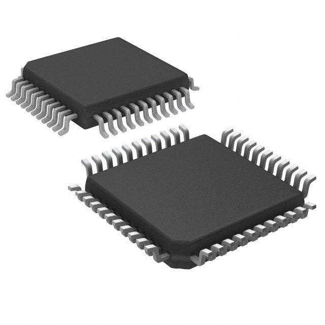
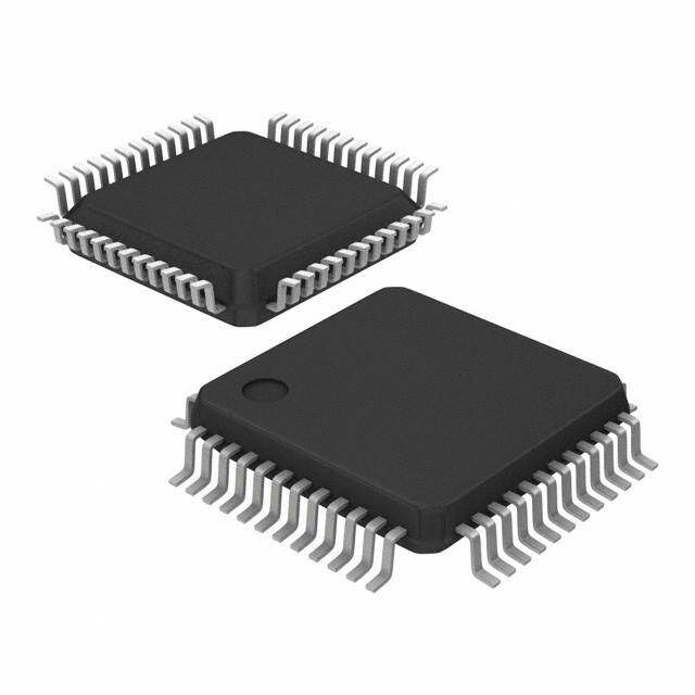
ICGOO在线商城 > 集成电路(IC) > 嵌入式 - 微控制器 > AT90PWM3B-16MUR
- 型号: AT90PWM3B-16MUR
- 制造商: Atmel
- 库位|库存: xxxx|xxxx
- 要求:
| 数量阶梯 | 香港交货 | 国内含税 |
| +xxxx | $xxxx | ¥xxxx |
查看当月历史价格
查看今年历史价格
AT90PWM3B-16MUR产品简介:
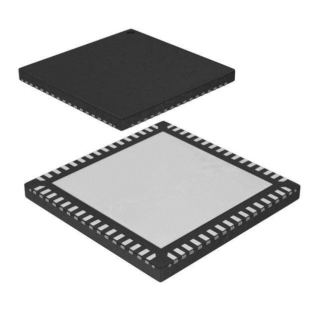
ICGOO电子元器件商城为您提供AT90PWM3B-16MUR由Atmel设计生产,在icgoo商城现货销售,并且可以通过原厂、代理商等渠道进行代购。 AT90PWM3B-16MUR价格参考。AtmelAT90PWM3B-16MUR封装/规格:嵌入式 - 微控制器, AVR 微控制器 IC AVR® 90PWM 照明 8-位 16MHz 8KB(8K x 8) 闪存 32-QFN(7x7)。您可以下载AT90PWM3B-16MUR参考资料、Datasheet数据手册功能说明书,资料中有AT90PWM3B-16MUR 详细功能的应用电路图电压和使用方法及教程。
| 参数 | 数值 |
| 产品目录 | 集成电路 (IC) |
| 描述 | IC MCU 8BIT 8KB FLASH 32QFN |
| EEPROM容量 | 512 x 8 |
| 产品分类 | |
| I/O数 | 27 |
| 品牌 | Atmel |
| 数据手册 | |
| 产品图片 |
|
| 产品型号 | AT90PWM3B-16MUR |
| PCN其它 | |
| RAM容量 | 512 x 8 |
| rohs | 无铅 / 符合限制有害物质指令(RoHS)规范要求 |
| 产品系列 | AVR® 90PWM 照明 |
| 产品培训模块 | http://www.digikey.cn/PTM/IndividualPTM.page?site=cn&lang=zhs&ptm=24997http://www.digikey.cn/PTM/IndividualPTM.page?site=cn&lang=zhs&ptm=25692http://www.digikey.cn/PTM/IndividualPTM.page?site=cn&lang=zhs&ptm=26162http://www.digikey.cn/PTM/IndividualPTM.page?site=cn&lang=zhs&ptm=26159http://www.digikey.cn/PTM/IndividualPTM.page?site=cn&lang=zhs&ptm=26180 |
| 供应商器件封装 | 32-QFN |
| 其它名称 | AT90PWM3B-16MUR-ND |
| 包装 | 带卷 (TR) |
| 外设 | 欠压检测/复位,POR,PWM,WDT |
| 封装/外壳 | 32-VFQFN 裸露焊盘 |
| 工作温度 | -40°C ~ 105°C |
| 振荡器类型 | 内部 |
| 数据转换器 | A/D 11x10b; D/A 1x10b |
| 标准包装 | 4,000 |
| 核心处理器 | AVR |
| 核心尺寸 | 8-位 |
| 电压-电源(Vcc/Vdd) | 2.7 V ~ 5.5 V |
| 程序存储器类型 | 闪存 |
| 程序存储容量 | 8KB(8K x 8) |
| 连接性 | SPI,UART/USART |
| 速度 | 16MHz |
| 配用 | /product-detail/zh/ATSTK600-SOIC/ATSTK600-SOIC-ND/1812228/product-detail/zh/ATAVRMC200/ATAVRMC200-ND/1118920/product-detail/zh/ATAVRFBKIT/ATAVRFBKIT-ND/1086725/product-detail/zh/ATSTK520/ATSTK520-ND/804782 |



PDF Datasheet 数据手册内容提取
Features • High Performance, Low Power Atmel® AVR® 8-bit Microcontroller (cid:129) Advanced RISC Architecture – 129 Powerful Instructions - Most Single Clock Cycle Execution – 32 x 8 General Purpose Working Registers – Fully Static Operation – Up to 1 MIPS throughput per MHz – On-chip 2-cycle Multiplier (cid:129) Data and Non-Volatile Program Memory 8-bit Atmel – 8K Bytes Flash of In-System Programmable Program Memory (cid:129) Endurance: 10,000 Write/Erase Cycles Microcontroller – Optional Boot Code Section with Independent Lock Bits (cid:129) In-System Programming by On-chip Boot Program with 8K Bytes (cid:129) True Read-While-Write Operation – 512 Bytes of In-System Programmable EEPROM In-System (cid:129) Endurance: 100,000 Write/Erase Cycles Programmable – 512 Bytes Internal SRAM – Programming Lock for Flash Program and EEPROM Data Security Flash (cid:129) On Chip Debug Interface (debugWIRE) (cid:129) Peripheral Features – Two or three 12-bit High Speed PSC (Power Stage Controllers) with 4-bit Resolution Enhancement AT90PWM2 (cid:129) Non Overlapping Inverted PWM Output Pins With Flexible Dead-Time (cid:129) Variable PWM duty Cycle and Frequency AT90PWM3 (cid:129) Synchronous Update of all PWM Registers (cid:129) Auto Stop Function for Event Driven PFC Implementation (cid:129) Less than 25 Hz Step Width at 150 kHz Output Frequency (cid:129) PSC2 with four Output Pins and Output Matrix – One 8-bit General purpose Timer/Counter with Separate Prescaler and Capture AT90PWM2B Mode – One 16-bit General purpose Timer/Counter with Separate Prescaler, Compare AT90PWM3B Mode and Capture Mode – Programmable Serial USART (cid:129) Standard UART mode (cid:129) 16/17 bit Biphase Mode for DALI Communications Summary – Master/Slave SPI Serial Interface – 10-bit ADC (cid:129) Up To 11 Single Ended Channels and 2 Fully Differential ADC Channel Pairs (cid:129) Programmable Gain (5x, 10x, 20x, 40x on Differential Channels) (cid:129) Internal Reference Voltage – 10-bit DAC – Two or three Analog Comparator with Resistor-Array to Adjust Comparison Voltage – 4 External Interrupts – Programmable Watchdog Timer with Separate On-Chip Oscillator (cid:129) Special Microcontroller Features – Low Power Idle, Noise Reduction, and Power Down Modes – Power On Reset and Programmable Brown Out Detection – Flag Array in Bit-programmable I/O Space (4 bytes) 4317KS–AVR–03/2013
AT90PWM2/3/2B/3B – In-System Programmable via SPI Port – Internal Calibrated RC Oscillator (8 MHz) – On-chip PLL for fast PWM (32 MHz, 64 MHz) and CPU (16 MHz) (cid:129) Operating Voltage: 2.7V - 5.5V (cid:129) Extended Operating Temperature: – -40C to +105C 12 bit PWM with ADC ADC Analog Product Package deadtime Input Diff Compar Application AT90PWM2 SO24 2 x 2 8 1 2 One fluorescent ballast AT90PWM2B AT90PWM3 SO32, HID ballast, fluorescent ballast, 3 x 2 11 2 3 AT90PWM3B QFN32 Motor control 1. History Product Revision AT90PWM2 First revision of parts, only for running production. AT90PWM3 Second revision of parts, for all new developments. The major changes are : (cid:129) complement the PSCOUT01, PSCOUT11, PSCOUT21 polarity in centered mode - See “PSCn0 & PSCn1 Basic Waveforms in Center Aligned Mode” on page 140. (cid:129) Add the PSC software triggering capture - See “PSC 0 Input Capture Register – PICR0H and PICR0L” on page 171. AT90PWM2B AT90PWM3B (cid:129) Add bits to read the PSC output activity - See “PSC0 Interrupt Flag Register – PIFR0” on page 173. (cid:129) Add some clock configurations - See “Device Clocking Options Select AT90PWM2B/3B” on page 31. (cid:129) Change Amplifier Synchonization - See “Amplifier” on page 252. and See “” on page 254. (cid:129) Correction of the Errata - See “Errata” on page 351. This datasheet deals with product characteristics of AT90PW2 and AT90WM3. It will be updated as soon as characterization will be done. 2. Disclaimer Typical values contained in this datasheet are based on simulations and characterization of other AVR microcontrollers manufactured on the same process technology. Min and Max val- ues will be available after the device is characterized. 2 4317KS–AVR–03/2013
AT90PWM2/3/2B/3B 3. Pin Configurations Figure 3-1. SOIC 24-pin Package AT90PWM2/2B SOIC24 (PSCOUT00/XCK/SS_A) PD0 1 24 PB7(ADC4/PSCOUT01/SCK) (RESET/OCD) PE0 2 23 PB6 (ADC7/ICP1B) (PSCIN0/CLKO) PD1 3 22 PB5 (ADC6/INT2) (PSCIN2/OC1A/MISO_A) PD2 4 21 PB4 (AMP0+) (TXD/DALI/OC0A/SS/MOSI_A) PD3 5 20 PB3 (AMP0-) VCC 6 19 AREF GND 7 18 AGND (MISO/PSCOUT20) PB0 8 17 AVCC (MOSI/PSCOUT21) PB1 9 16 PB2 (ADC5/INT1) (OC0B/XTAL1) PE1 10 15 PD7 (ACMP0) (ADC0/XTAL2) PE2 11 14 PD6 (ADC3/ACMPM/INT0) (ADC1/RXD/DALI/ICP1A/SCK_A) PD4 12 13 PD5 (ADC2/ACMP2) Figure 3-2. SOIC 32-pin Package AT90PWM3/3B SOIC 32 (PSCOUT00/XCK/SS_A) PD0 1 32 PB7(ADC4/PSCOUT01/SCK) (INT3/PSCOUT10) PC0 2 31 PB6 (ADC7/PSCOUT11/ICP1B) (RESET/OCD) PE0 3 30 PB5 (ADC6/INT2) (PSCIN0/CLKO) PD1 4 29 PC7 (D2A) (PSCIN2/OC1A/MISO_A) PD2 5 28 PB4 (AMP0+) (TXD/DALI/OC0A/SS/MOSI_A) PD3 6 27 PB3 (AMP0-) (PSCIN1/OC1B) PC1 7 26 PC6 (ADC10/ACMP1) VCC 8 25 AREF GND 9 24 AGND (T0/PSCOUT22) PC2 10 23 AVCC (T1/PSCOUT23) PC3 11 22 PC5 (ADC9/AMP1+) (MISO/PSCOUT20) PB0 12 21 PC4 (ADC8/AMP1-) (MOSI/PSCOUT21) PB1 13 20 PB2 (ADC5/INT1) (OC0B/XTAL1) PE1 14 19 PD7 (ACMP0) (ADC0/XTAL2) PE2 15 18 PD6 (ADC3/ACMPM/INT0) (ADC1/RXD/DALI/ICP1A/SCK_A) PD4 16 17 PD5 (ADC2/ACMP2) 3 4317KS–AVR–03/2013
AT90PWM2/3/2B/3B Figure 3-3. QFN32 (7*7 mm) Package. AT90PWM3/3B QFN 32 B) A) K) 1 _ C P S S C 0) K/S 01/ 11/I CIN0/CLKO) SET/OCD) 3/PSCOUT1 COUT00/XC C4/PSCOUT C7/PSCOUT C6/INT2) A) PS RE NT PS AD AD AD D2 (1 (0 (I0 (0 7 ( 6 ( 5 ( 7 ( D E C D B B B C P P P P P P P P 2 1 0 9 8 7 6 5 3 3 3 2 2 2 2 2 (PSCIN2/OC1A/MISO_A) PD2 1 24 PB4 (AMP0+) (TXD/DALI/OC0A/SS/MOSI_A) PD3 2 23 PB3 (AMP0-) (PSCIN1/OC1B) PC1 3 22 PC6 (ADC10/ACMP1) VCC 4 21 AREF GND 5 20 AGND (T0/PSCOUT22) PC2 6 19 AVCC (T1/PSCOUT23) PC3 7 18 PC5 (ADC9/AMP1+) (MISO/PSCOUT20) PB0 8 17 PC4 (ADC8/AMP1-) 0 1 2 3 4 5 6 9 1 1 1 1 1 1 1 1 1 2 4 5 6 7 2 B E E D D D D B P P P P P P P P (MOSI/PSCOUT21) (OC0B/XTAL1) (ADC0/XTAL2) D/DALI/ICP1_A/SCK_A) (ADC2/ACMP2 ) (ADC3/ACMPM/INT0) (ACMP0) (ADC5/INT1) X R 1/ C D A ( Note: The Center GND PADDLE has to be connected to GND. 4 4317KS–AVR–03/2013
AT90PWM2/3/2B/3B 3.1 Pin Descriptions Table 3-1. Pin out description S024 Pin SO32 Pin QFN32 Pin Number Number Number Mnemonic Type Name, Function & Alternate Function 7 9 5 GND Power Ground: 0V reference 18 24 20 AGND Power Analog Ground: 0V reference for analog part 6 8 4 VCC power Power Supply: Analog Power Supply: This is the power supply voltage for analog 17 23 19 AVCC Power part For a normal use this pin must be connected. Analog Reference : reference for analog converter . This is the 19 25 21 AREF Power reference voltage of the A/D converter. As output, can be used by external analog MISO (SPI Master In Slave Out) 8 12 8 PBO I/O PSCOUT20 output MOSI (SPI Master Out Slave In) 9 13 9 PB1 I/O PSCOUT21 output ADC5 (Analog Input Channel5 ) 16 20 16 PB2 I/O INT1 20 27 23 PB3 I/O AMP0- (Analog Differential Amplifier 0 Input Channel ) 21 28 24 PB4 I/O AMP0+ (Analog Differential Amplifier 0 Input Channel ) ADC6 (Analog Input Channel 6) 22 30 26 PB5 I/O INT 2 ADC7 (Analog Input Channel 7) 23 31 27 PB6 I/O ICP1B (Timer 1 input capture alternate input) PSCOUT11 output (see note 1) PSCOUT01 output 24 32 28 PB7 I/O ADC4 (Analog Input Channel 4) SCK (SPI Clock) 5 4317KS–AVR–03/2013
AT90PWM2/3/2B/3B Table 3-1. Pin out description (Continued) S024 Pin SO32 Pin QFN32 Pin Number Number Number Mnemonic Type Name, Function & Alternate Function PSCOUT10 output (see note 1) 2 30 PC0 I/O INT3 PSCIN1 (PSC 1 Digital Input) 7 3 PC1 I/O OC1B (Timer 1 Output Compare B) T0 (Timer 0 clock input) 10 6 PC2 I/O PSCOUT22 output T1 (Timer 1 clock input) 11 7 PC3 I/O NA PSCOUT23 output ADC8 (Analog Input Channel 8) 21 17 PC4 I/O AMP1- (Analog Differential Amplifier 1 Input Channel ) ADC9 (Analog Input Channel 9) 22 18 PC5 I/O AMP1+ (Analog Differential Amplifier 1 Input Channel ) ADC10 (Analog Input Channel 10) 26 22 PC6 I/O ACMP1 (Analog Comparator 1 Positive Input ) 29 25 PC7 I/O D2A : DAC output PSCOUT00 output 1 1 29 PD0 I/O XCK (UART Transfer Clock) SS_A (Alternate SPI Slave Select) PSCIN0 (PSC 0 Digital Input ) 3 4 32 PD1 I/O CLKO (System Clock Output) PSCIN2 (PSC 2 Digital Input) 4 5 1 PD2 I/O OC1A (Timer 1 Output Compare A) MISO_A (Programming & alternate SPI Master In Slave Out) TXD (Dali/UART Tx data) OC0A (Timer 0 Output Compare A) 5 6 2 PD3 I/O SS (SPI Slave Select) MOSI_A (Programming & alternate Master Out SPI Slave In) ADC1 (Analog Input Channel 1) RXD (Dali/UART Rx data) 12 16 12 PD4 I/O ICP1A (Timer 1 input capture) SCK_A (Programming & alternate SPI Clock) ADC2 (Analog Input Channel 2) 13 17 13 PD5 I/O ACMP2 (Analog Comparator 2 Positive Input ) ADC3 (Analog Input Channel 3 ) 14 18 14 PD6 I/O ACMPM reference for analog comparators INT0 15 19 15 PD7 I/O ACMP0 (Analog Comparator 0 Positive Input ) RESET (Reset Input) 2 3 31 PE0 I/O or I OCD (On Chip Debug I/O) XTAL1: XTAL Input 10 14 10 PE1 I/O OC0B (Timer 0 Output Compare B) 6 4317KS–AVR–03/2013
AT90PWM2/3/2B/3B Table 3-1. Pin out description (Continued) S024 Pin SO32 Pin QFN32 Pin Number Number Number Mnemonic Type Name, Function & Alternate Function XTAL2: XTAL OuTput 11 15 11 PE2 I/O ADC0 (Analog Input Channel 0) 1. PSCOUT10 & PSCOUT11 are not present on 24 pins package 4. Overview The AT90PWM2/2B/3/3B is a low-power CMOS 8-bit microcontroller based on the AVR enhanced RISC architecture. By executing powerful instructions in a single clock cycle, the AT90PWM2/2B/3/3B achieves throughputs approaching 1 MIPS per MHz allowing the system designer to optimize power consumption versus processing speed. 7 4317KS–AVR–03/2013
AT90PWM2/3/2B/3B 4.1 Block Diagram Figure 4-1. Block Diagram Data Bus 8-bit Program Status Interrupt 8Kx8 Flash Counter and Control Unit Program Memory SPI Unit 32 x 8 Instruction General Watchdog Register Purpose Timer Registrers 3 Analog Instruction Comparators Decoder g g n ssin essi ALU DALI USART Control Lines dre ddr d A Direct A ndirect Timer 0 I Timer 1 Data SRAM 512 bytes ADC EEPROM 512 bytes DAC I/O Lines PSC 2/1/0 The AVR core combines a rich instruction set with 32 general purpose working registers. All the 32 registers are directly connected to the Arithmetic Logic Unit (ALU), allowing two independent registers to be accessed in one single instruction executed in one clock cycle. The resulting architecture is more code efficient while achieving throughputs up to ten times faster than con- ventional CISC microcontrollers. The AT90PWM2/2B/3/3B provides the following features: 8K bytes of In-System Programmable Flash with Read-While-Write capabilities, 512 bytes EEPROM, 512 bytes SRAM, 53 general purpose I/O lines, 32 general purpose working registers, three Power Stage Controllers, two flexible Timer/Counters with compare modes and PWM, one USART with DALI mode, an 11- channel 10-bit ADC with two differential input stage with programmable gain, a 10-bit DAC, a programmable Watchdog Timer with Internal Oscillator, an SPI serial port, an On-chip Debug system and four software selectable power saving modes. 8 4317KS–AVR–03/2013
AT90PWM2/3/2B/3B The Idle mode stops the CPU while allowing the SRAM, Timer/Counters, SPI ports and interrupt system to continue functioning. The Power-down mode saves the register contents but freezes the Oscillator, disabling all other chip functions until the next interrupt or Hardware Reset. The ADC Noise Reduction mode stops the CPU and all I/O modules except ADC, to minimize switch- ing noise during ADC conversions. In Standby mode, the Crystal/Resonator Oscillator is running while the rest of the device is sleeping. This allows very fast start-up combined with low power consumption. The device is manufactured using Atmel’s high-density nonvolatile memory technology. The On- chip ISP Flash allows the program memory to be reprogrammed in-system through an SPI serial interface, by a conventional nonvolatile memory programmer, or by an On-chip Boot program running on the AVR core. The boot program can use any interface to download the application program in the application Flash memory. Software in the Boot Flash section will continue to run while the Application Flash section is updated, providing true Read-While-Write operation. By combining an 8-bit RISC CPU with In-System Self-Programmable Flash on a monolithic chip, the Atmel AT90PWM2/3 is a powerful microcontroller that provides a highly flexible and cost effective solution to many embedded control applications. The AT90PWM2/3 AVR is supported with a full suite of program and system development tools including: C compilers, macro assemblers, program debugger/simulators, in-circuit emulators, and evaluation kits. 4.2 Pin Descriptions 4.2.1 VCC Digital supply voltage. 4.2.2 GND Ground. 4.2.3 Port B (PB7..PB0) Port B is an 8-bit bi-directional I/O port with internal pull-up resistors (selected for each bit). The Port B output buffers have symmetrical drive characteristics with both high sink and source capability. As inputs, Port B pins that are externally pulled low will source current if the pull-up resistors are activated. The Port B pins are tri-stated when a reset condition becomes active, even if the clock is not running. Port B also serves the functions of various special features of the AT90PWM2/2B/3/3B as listed on page 69. 4.2.4 Port C (PC7..PC0) Port C is an 8-bit bi-directional I/O port with internal pull-up resistors (selected for each bit). The Port C output buffers have symmetrical drive characteristics with both high sink and source capability. As inputs, Port C pins that are externally pulled low will source current if the pull-up resistors are activated. The Port C pins are tri-stated when a reset condition becomes active, even if the clock is not running. Port C is not available on 24 pins package. Port C also serves the functions of special features of the AT90PWM2/2B/3/3B as listed on page 72. 9 4317KS–AVR–03/2013
AT90PWM2/3/2B/3B 4.2.5 Port D (PD7..PD0) Port D is an 8-bit bi-directional I/O port with internal pull-up resistors (selected for each bit). The Port D output buffers have symmetrical drive characteristics with both high sink and source capability. As inputs, Port D pins that are externally pulled low will source current if the pull-up resistors are activated. The Port D pins are tri-stated when a reset condition becomes active, even if the clock is not running. Port D also serves the functions of various special features of the AT90PWM2/2B/3/3B as listed on page 75. 4.2.6 Port E (PE2..0) RESET/ XTAL1/ XTAL2 Port E is an 3-bit bi-directional I/O port with internal pull-up resistors (selected for each bit). The Port E output buffers have symmetrical drive characteristics with both high sink and source capability. As inputs, Port E pins that are externally pulled low will source current if the pull-up resistors are activated. The Port E pins are tri-stated when a reset condition becomes active, even if the clock is not running. If the RSTDISBL Fuse is programmed, PE0 is used as an I/O pin. Note that the electrical char- acteristics of PE0 differ from those of the other pins of Port C. If the RSTDISBL Fuse is unprogrammed, PE0 is used as a Reset input. A low level on this pin for longer than the minimum pulse length will generate a Reset, even if the clock is not running. The minimum pulse length is given in Table 9-1 on page 47. Shorter pulses are not guaranteed to generate a Reset. Depending on the clock selection fuse settings, PE1 can be used as input to the inverting Oscil- lator amplifier and input to the internal clock operating circuit. Depending on the clock selection fuse settings, PE2 can be used as output from the inverting Oscillator amplifier. The various special features of Port E are elaborated in “Alternate Functions of Port E” on page 78 and “Clock Systems and their Distribution” on page 29. 4.2.7 AVCC AVCC is the supply voltage pin for the A/D Converter. It should be externally connected to V , CC even if the ADC is not used. If the ADC is used, it should be connected to V through a low- CC pass filter. 4.2.8 AREF This is the analog reference pin for the A/D Converter. 4.3 About Code Examples This documentation contains simple code examples that briefly show how to use various parts of the device. These code examples assume that the part specific header file is included before compilation. Be aware that not all C compiler vendors include bit definitions in the header files and interrupt handling in C is compiler dependent. Please confirm with the C compiler documen- tation for more details. 10 4317KS–AVR–03/2013
AT90PWM2/3/2B/3B 5. Ordering Information Speed (MHz) Power Supply Ordering Code Package Operation Range 16 2.7 - 5.5V AT90PWM3-16SQ SO32 Extended (-40C to 105C) 16 2.7 - 5.5V AT90PWM3-16MQT QFN32 Extended (-40C to 105C) 16 2.7 - 5.5V AT90PWM3-16MQ QFN32 Extended (-40C to 105C) 16 2.7 - 5.5V AT90PWM2-16SQ SO24 Extended (-40C to 105C) 16 2.7 - 5.5V AT90PWM3B-16SE SO32 Engineering Samples 16 2.7 - 5.5V AT90PWM3B-16ME QFN32 Engineering Samples 16 2.7 - 5.5V AT90PWM2B-16SE SO24 Engineering Samples 16 2.7 - 5.5V AT90PWM3B-16SU SO32 Extended (-40C to 105C) 16 2.7 - 5.5V AT90PWM3B-16MU QFN32 Extended (-40C to 105C) 16 2.7 - 5.5V AT90PWM2B-16SU SO24 Extended (-40C to 105C) Note: All packages are Pb free, fully LHF Note: This device can also be supplied in wafer form. Please contact your local Atmel sales office for detailed ordering information and minimum quantities. Note: Parts numbers are for shipping in sticks (SO) or in trays (QFN). These devices can also be supplied in Tape and Reel. Please contact your local Atmel sales office for detailed ordering information and minimum quantities. Note: 16MQT = Trays Note: 16MQ = Tape and Reel Note: PWM2 is not recommended for new designs, use PWM2B for your developments Note: PWM3 is not recommended for new designs, use PWM3B for your developments 11 4317KS–AVR–03/2013
AT90PWM2/3/2B/3B 6. Package Information Package Type SO24 24-Lead, Small Outline Package SO32 32-Lead, Small Outline Package QFN32 32-Lead, Quad Flat No lead 12 4317KS–AVR–03/2013
AT90PWM2/3/2B/3B 6.1 SO24 13 4317KS–AVR–03/2013
AT90PWM2/3/2B/3B 6.2 SO32 14 4317KS–AVR–03/2013
AT90PWM2/3/2B/3B 6.3 QFN32 15 4317KS–AVR–03/2013
AT90PWM2/3/2B/3B 16 4317KS–AVR–03/2013
AT90PWM2/3/2B/3B 7. Errata 7.1 AT90PWM2&3 Rev. A (Mask Revision) (cid:129) PGM: PSCxRB Fuse (cid:129) PSC: Prescaler (cid:129) PSC: PAOCnA and PAOCnB Register Bits (Asynchronous output control) (cid:129) PSC: PEVxA/B Flag Bits (cid:129) PSC: Output Polarity in Centered Mode (cid:129) PSC: Output Activity (cid:129) VREF (cid:129) DALI (cid:129) DAC: Register Update (cid:129) DAC: Output spikes (cid:129) DAC driver: Output Voltage linearity (cid:129) ADC: Conversion accuracy (cid:129) Analog comparator: Offset value (cid:129) Analog comparator: Output signal (cid:129) PSC: Autolock modes (cid:129) DALI: 17th bit detection (cid:129) PSC: One ramp mode with PSC input mode 8 1. PGM: PSCnRB Fuse The use of PSCnRB fuse can make the parallel ISP fail. Workaround: When PSCnRB fuses are used, use the serial programming mode to load a new program version. 2. PSC: Prescaler The use of PSC's prescaler have the following effects : It blocks the sample of PSC inputs until the two first cycles following the set of PSC run bit. A fault is not properly transferred to other (slave) PSC. Workaround: Clear the prescaler PPREx bit when stopping the PSC (prun = 0), and set them to appropri- ate value when starting the PSC (prun = 1), these bits are in the same PCTL register Do not use the prescaler when a fault on one PSC should affect other PSC’s 3. PSC: PAOCnA and PAOCnB Register Bits (Asynchronous output control) These register bits are malfunctioning. Workaround: Do not use this feature. 4. PSC: PEVnA/B flag bits These flags are set when a fault arises, but can also be set again during the fault itself. Workaround: Don't clear these flags before the fault disappears. 17 4317KS–AVR–03/2013
AT90PWM2/3/2B/3B 5. PSC: Output Polarity in Centered Mode In centered mode, PSCOUTn1 outputs are not inverted, so they are active at the same time as PSCOUTn0. Workaround: Use an external inverter (or a driver with inverting output) to drive the load on PSCOUTn1. 6. PSC : POACnA/B Output Activity These register bits are not implemented in rev A. Workaround: Do not use this feature. 7. VREF Remark: To have Internal Vref on AREF pin select an internal analog feature such as DAC or ADC. Some stand by power consuption may be observed if Vref equals AVcc 8. DALI Some troubles on Dali extension when edges are not symmetric. Workaround: Use an optocoupler providing symmetric edges on Rx and Tx DALI lines (only recom- manded for software validation purpose). 9. DAC: Register Update Registers DACL & DACH are not written when the DAC is not enabled. Workaround: Enable DAC with DAEN before writing in DACL & DACH. To prevent an unwanted zero out- put on DAC pin, enable DAC output, with DAOE afterwards. 10. DAC : Output spikes During transition between two codes, a spike may appears Work around: Filter spike or wait for steady state No spike appears if the 4 last signifiant bits remain zero. 11. DAC driver: Output Voltage linearity The voltage linearity of the DAC driver is limited when the DAC output goes above Vcc - 1V. Work around: Do not use AVcc as Vref ; internal Vref gives good results 12. ADC : Conversion accuracy The conversion accuracy degrades when the ADC clock is 1 & 2 MHz. Work around: When a 10 bit conversion accuracy is required, use an ADC clock of 500 kHz or below. 13. Analog comparator: Offset value The offset value increases when the common mode voltage is above Vcc - 1.5V. Work around: Limit common mode voltage 18 4317KS–AVR–03/2013
AT90PWM2/3/2B/3B 14. Analog comparator: Output signal The comparator output toggles at the comparator clock frequency when the voltage differ- ence between both inputs is lower than the offset. This may occur when comparing signal with small slew rate. Work around: This effect normally do not impact the PSC, as the transition is sampled once per PSC cycle Be carefull when using the comparator as an interrupt source. 15. PSC : Autolock mode This mode is not properly handled when CLKPSC is different from CLK IO. Work around: With CLKPSC equals 64/32 MHz (CLKPLL), use LOCK mode 16. DALI : 17th bit detection 17th bit detection do not occurs if the signal arrives after the sampling point. Workaround: Use this feature only for sofware development and not in field conditions 17. PSC : One ramp mode with PSC input mode 8 The retriggering is not properly handled in this case. Work around: Do not program this case. 18. PSC : Desactivation of outputs in mode 14 See “PSC Input Mode 14: Fixed Frequency Edge Retrigger PSC and Disactivate Output” on page 156. Work around: Do not use this mode to desactivate output if retrigger event do not occurs during On-Time. 7.2 AT90PWM2B/3B (cid:129) PSC : Double End-Of-Cycle Interrupt Request in Centered Mode • ADC : Conversion accuracy 1. PSC : Double End-Of-Cycle Interrupt Request in Centered Mode In centered mode, after the “expected” End-Of-Cycle Interrupt, a second unexpected Inter- rupt occurs 1 PSC cycle after the previous interrupt. Work around: While CPU cycle is lower than PSC clock, the CPU sees only one interrupt request. For PSC clock period greater than CPU cycle, the second interrupt request must be cleared by software. 2. ADC : Conversion accuracy The conversion accuracy degrades when the ADC clock is 2 MHz. Work around: When a 10 bit conversion accuracy is required, use an ADC clock of 1 MHz or below. At 2 Mhz the ADC can be used as a 7 bits ADC. 3. DAC Driver linearity above 3.6V With 5V Vcc, the DAC driver linearity is poor when DAC output level is above Vcc-1V. At 5V, DAC output for 1023 will be around 5V - 40mV. 19 4317KS–AVR–03/2013
AT90PWM2/3/2B/3B Work around: . Use, when Vcc=5V, Vref below Vcc-1V. Or, when Vref=Vcc=5V, do not uses codes above 800. 4. DAC Update in Autotrig mode If the cpu writes in DACH register at the same instant that the selected trigger source occurs and DAC Auto Trigger is enabled, the DACH register is not updated by the new value. Work around: . When using the autotrig mode, write twice in the DACH register. The time between the two CPU writes, must be different than the trigger source frequency. 20 4317KS–AVR–03/2013
AT90PWM2/3/2B/3B 8. Errata 8.1 AT90PWM2&3 Rev. A (Mask Revision) (cid:129) PGM: PSCxRB Fuse (cid:129) PSC: Prescaler (cid:129) PSC: PAOCnA and PAOCnB Register Bits (Asynchronous output control) (cid:129) PSC: PEVxA/B Flag Bits (cid:129) PSC: Output Polarity in Centered Mode (cid:129) PSC: Output Activity (cid:129) VREF (cid:129) DALI (cid:129) DAC: Register Update (cid:129) DAC: Output spikes (cid:129) DAC driver: Output Voltage linearity (cid:129) ADC: Conversion accuracy (cid:129) Analog comparator: Offset value (cid:129) Analog comparator: Output signal (cid:129) PSC: Autolock modes (cid:129) DALI: 17th bit detection (cid:129) PSC: One ramp mode with PSC input mode 8 1. PGM: PSCnRB Fuse The use of PSCnRB fuse can make the parallel ISP fail. Workaround: When PSCnRB fuses are used, use the serial programming mode to load a new program version. 2. PSC: Prescaler The use of PSC's prescaler have the following effects: It blocks the sample of PSC inputs until the two first cycles following the set of PSC run bit. A fault is not properly transferred to other (slave) PSC. Workaround: Clear the prescaler PPREx bit when stopping the PSC (prun = 0), and set them to appropri- ate value when starting the PSC (prun = 1), these bits are in the same PCTL register Do not use the prescaler when a fault on one PSC should affect other PSC’s 3. PSC: PAOCnA and PAOCnB Register Bits (Asynchronous output control) These register bits are malfunctioning. Workaround: Do not use this feature. 4. PSC: PEVnA/B flag bits These flags are set when a fault arises, but can also be set again during the fault itself. Workaround: Don't clear these flags before the fault disappears. 21 4317KS–AVR–03/2013
AT90PWM2/3/2B/3B 5. PSC: Output Polarity in Centered Mode In centered mode, PSCOUTn1 outputs are not inverted, so they are active at the same time as PSCOUTn0. Workaround: Use an external inverter (or a driver with inverting output) to drive the load on PSCOUTn1. 6. PSC: POACnA/B Output Activity These register bits are not implemented in rev A. Workaround: Do not use this feature. 7. VREF Remark: To have Internal Vref on AREF pin select an internal analog feature such as DAC or ADC. Some stand by power consuption may be observed if Vref equals AVcc 8. DALI Some troubles on Dali extension when edges are not symmetric. Workaround: Use an optocoupler providing symmetric edges on Rx and Tx DALI lines (only recom- manded for software validation purpose). 9. DAC: Register Update Registers DACL & DACH are not written when the DAC is not enabled. Workaround: Enable DAC with DAEN before writing in DACL & DACH. To prevent an unwanted zero out- put on DAC pin, enable DAC output, with DAOE afterwards. 10. DAC : Output spikes During transition between two codes, a spike may appears Work around: Filter spike or wait for steady state No spike appears if the 4 last signifiant bits remain zero. 11. DAC driver: Output Voltage linearity The voltage linearity of the DAC driver is limited when the DAC output goes above Vcc - 1V. Work around: Do not use AVcc as Vref ; internal Vref gives good results 12. ADC : Conversion accuracy The conversion accuracy degrades when the ADC clock is 1 & 2 MHz. Work around: When a 10 bit conversion accuracy is required, use an ADC clock of 500 kHz or below. 13. Analog comparator: Offset value The offset value increases when the common mode voltage is above Vcc - 1.5V. Work around: Limit common mode voltage 22 4317KS–AVR–03/2013
AT90PWM2/3/2B/3B 14. Analog comparator: Output signal The comparator output toggles at the comparator clock frequency when the voltage differ- ence between both inputs is lower than the offset. This may occur when comparing signal with small slew rate. Work around: This effect normally do not impact the PSC, as the transition is sampled once per PSC cycle Be careful when using the comparator as an interrupt source. 15. PSC : Autolock mode This mode is not properly handled when CLKPSC is different from CLK IO. Work around: With CLKPSC equals 64/32 MHz (CLKPLL), use LOCK mode 16. DALI : 17th bit detection 17th bit detection do not occurs if the signal arrives after the sampling point. Workaround: Use this feature only for sofware development and not in field conditions 17. PSC : One ramp mode with PSC input mode 8 The retriggering is not properly handled in this case. Work around: Do not program this case. 18. PSC : Desactivation of outputs in mode 14 See “PSC Input Mode 14: Fixed Frequency Edge Retrigger PSC and Disactivate Output” on page 156. Work around: Do not use this mode to deactivate output if retrigger event do not occurs during On-Time. 8.2 AT90PWM2B/3B (cid:129) PSC : Double End-Of-Cycle Interrupt Request in Centered Mode • ADC : Conversion accuracy 1. PSC : Double End-Of-Cycle Interrupt Request in Centered Mode In centered mode, after the “expected” End-Of-Cycle Interrupt, a second unexpected Inter- rupt occurs 1 PSC cycle after the previous interrupt. Work around: While CPU cycle is lower than PSC clock, the CPU sees only one interrupt request. For PSC clock period greater than CPU cycle, the second interrupt request must be cleared by software. 2. ADC : Conversion accuracy The conversion accuracy degrades when the ADC clock is 2 MHz. Work around: When a 10 bit conversion accuracy is required, use an ADC clock of 1 MHz or below. At 2 Mhz the ADC can be used as a 7 bits ADC. 3. DAC Driver linearity above 3.6V With 5V Vcc, the DAC driver linearity is poor when DAC output level is above Vcc-1V. At 5V, DAC output for 1023 will be around 5V - 40mV. 23 4317KS–AVR–03/2013
AT90PWM2/3/2B/3B Work around: Use, when Vcc=5V, Vref below Vcc-1V. Or, when Vref=Vcc=5V, do not uses codes above 800. 4. DAC Update in Autotrig mode If the cpu writes in DACH register at the same instant that the selected trigger source occurs and DAC Auto Trigger is enabled, the DACH register is not updated by the new value. Work around: When using the autotrig mode, write twice in the DACH register. The time between the two CPU writes, must be different than the trigger source frequency. 24 4317KS–AVR–03/2013
Atmel Corporation Atmel Asia Limited Atmel Munich GmbH Atmel Japan G.K. 1600 Technology Drive Unit 01-5 & 16, 19F Business Campus 16F Shin-Osaki Kangyo Bldg San Jose, CA 95110 BEA Tower, Millennium City 5 Parkring 4 1-6-4 Osaki, Shinagawa-ku USA 418 Kwun Tong Roa D-85748 Garching b. Munich Tokyo 141-0032 Tel: (+1) (408) 441-0311 Kwun Tong, Kowloon GERMANY JAPAN Fax: (+1) (408) 487-2600 HONG KONG Tel: (+49) 89-31970-0 Tel: (+81) (3) 6417-0300 www.atmel.com Tel: (+852) 2245-6100 Fax: (+49) 89-3194621 Fax: (+81) (3) 6417-0370 Fax: (+852) 2722-1369 © 2013 Atmel Corporation. All rights reserved. / Rev.: 4317KS–AVR–03/2013 Atmel®, Atmel logo and combinations thereof, Enabling Unlimited Possibilities®, and others are registered trademarks or trademarks of Atmel Corporation or its subsidiaries. Other terms and product names may be trademarks of others. Disclaimer: The information in this document is provided in connection with Atmel products. No license, express or implied, by estoppel or otherwise, to any intellectual property right is granted by this document or in connection with the sale of Atmel products. EXCEPT AS SET FORTH IN THE ATMEL TERMS AND CONDITIONS OF SALES LOCATED ON THE ATMEL WEBSITE, ATMEL ASSUMES NO LIABILITY WHATSOEVER AND DISCLAIMS ANY EXPRESS, IMPLIED OR STATUTORY WARRANTY RELATING TO ITS PRODUCTS INCLUDING, BUT NOT LIMITED TO, THE IMPLIED WARRANTY OF MERCHANTABILITY, FITNESS FOR A PARTICULAR PURPOSE, OR NON-INFRINGEMENT. IN NO EVENT SHALL ATMEL BE LIABLE FOR ANY DIRECT, INDIRECT, CONSEQUENTIAL, PUNITIVE, SPECIAL OR INCIDENTAL DAMAGES (INCLUDING, WITHOUT LIMITATION, DAMAGES FOR LOSS AND PROFITS, BUSINESS INTERRUPTION, OR LOSS OF INFORMATION) ARISING OUT OF THE USE OR INABILITY TO USE THIS DOCUMENT, EVEN IF ATMEL HAS BEEN ADVISED OF THE POSSIBILITY OF SUCH DAMAGES. Atmel makes no representations or warranties with respect to the accuracy or completeness of the contents of this document and reserves the right to make changes to specifications and products descriptions at any time without notice. Atmel does not make any commitment to update the information contained herein. Unless specifically provided otherwise, Atmel products are not suitable for, and shall not be used in, automotive applications. Atmel products are not intended, authorized, or warranted for use as components in applications intended to support or sustain life.
Mouser Electronics Authorized Distributor Click to View Pricing, Inventory, Delivery & Lifecycle Information: M icrochip: AT90PWM3B-16MU AT90PWM3B-16SU AT90PWM3B-16SUR AT90PWM3-16SQ AT90PWM3-16MQ AT90PWM3-16MQT AT90PWM3B-16MUR
/AT90PWM3B-16MUR.jpg)
 Datasheet下载
%20Renders/32-VQFN%20Exposed%20Pad.jpg)


