ICGOO在线商城 > AT42QT1070-SSU
- 型号: AT42QT1070-SSU
- 制造商: Atmel
- 库位|库存: xxxx|xxxx
- 要求:
| 数量阶梯 | 香港交货 | 国内含税 |
| +xxxx | $xxxx | ¥xxxx |
查看当月历史价格
查看今年历史价格
AT42QT1070-SSU产品简介:
ICGOO电子元器件商城为您提供AT42QT1070-SSU由Atmel设计生产,在icgoo商城现货销售,并且可以通过原厂、代理商等渠道进行代购。 提供AT42QT1070-SSU价格参考以及AtmelAT42QT1070-SSU封装/规格参数等产品信息。 你可以下载AT42QT1070-SSU参考资料、Datasheet数据手册功能说明书, 资料中有AT42QT1070-SSU详细功能的应用电路图电压和使用方法及教程。
| 参数 | 数值 |
| 产品目录 | |
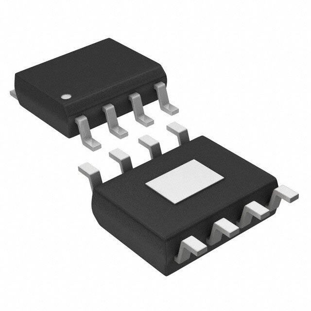
| 描述 | IC TOUCH SENSOR 7KEY 14SOIC电容触摸传感器 QTouch 7 Ch. Touch Sensor IC |
| 产品分类 | 电容式触摸传感器,接近传感器 IC电容触摸传感器 |
| 品牌 | Atmel |
| 产品手册 | |
| 产品图片 |
|
| rohs | 符合RoHS无铅 / 符合限制有害物质指令(RoHS)规范要求 |
| 产品系列 | Atmel AT42QT1070-SSUQTouch™ |
| 数据手册 | |
| 产品型号 | AT42QT1070-SSU |
| 产品种类 | 电容触摸传感器 |
| 供应商器件封装 | 14-SO |
| 其它名称 | AT42QT1070-SSU QS529DKR |
| 分辨率(位) | - |
| 包装 | Digi-Reel® |
| 参考设计库 | http://www.digikey.com/rdl/4294959886/4294959868/869 |
| 商标 | Atmel |
| 安装类型 | 表面贴装 |
| 封装/外壳 | 14-SOIC(0.154",3.90mm 宽) |
| 工作温度 | -40°C ~ 85°C |
| 工厂包装数量 | 3000 |
| 数据接口 | I²C |
| 数据速率/采样率(SPS,BPS) | - |
| 标准包装 | 1 |
| 电压-电源 | 1.8 V ~ 5.5 V |
| 电压基准 | 内部 |
| 电流-电源 | ±10mA |
| 类型 | 电容式开关 |
| 触摸面板接口 | - |
| 评估工具 | 可供 |
| 输入/按键数 | 7 键(Comms),5 键(独立式) |
| 配用 | /product-detail/zh/ATEVK1070B/ATEVK1070B-ND/2522740/product-detail/zh/ATEVK1070A/ATEVK1070A-ND/2522739 |





- 商务部:美国ITC正式对集成电路等产品启动337调查
- 曝三星4nm工艺存在良率问题 高通将骁龙8 Gen1或转产台积电
- 太阳诱电将投资9.5亿元在常州建新厂生产MLCC 预计2023年完工
- 英特尔发布欧洲新工厂建设计划 深化IDM 2.0 战略
- 台积电先进制程称霸业界 有大客户加持明年业绩稳了
- 达到5530亿美元!SIA预计今年全球半导体销售额将创下新高
- 英特尔拟将自动驾驶子公司Mobileye上市 估值或超500亿美元
- 三星加码芯片和SET,合并消费电子和移动部门,撤换高东真等 CEO
- 三星电子宣布重大人事变动 还合并消费电子和移动部门
- 海关总署:前11个月进口集成电路产品价值2.52万亿元 增长14.8%
.jpg)

PDF Datasheet 数据手册内容提取
Atmel AT42QT1070 Seven-channel QTouch® Touch Sensor IC DATASHEET Features Configurations: Comms mode Standalone mode Number of Keys: Comms mode: 1 – 7 keys (or 1 – 6 keys plus a Guard Channel) Standalone mode: 1 – 4 keys plus a fixed Guard Channel on key 0 Number of I/O Lines: Standalone mode: 5 outputs Technology: Patented spread-spectrum charge-transfer Key Outline Sizes: 6mmx 6mm or larger (panel thickness dependent); widely different sizes and shapes possible Layers Required: One Electrode Materials: Etched copper; Silver; Carbon; Indium Tin Oxide (ITO) Panel Materials: Plastic; Glass; Composites; Painted surfaces (low particle density metallic paints possible Panel Thickness: Up to 10mm glass; Up to 5mm plastic (electrode size dependent) Key Sensitivity: Comms mode: individually settable via simple commands over I2C-compatible interface Standalone mode: settings are fixed Interface: I2C-compatible slave mode (400kHz). Discrete detection outputs Signal Processing: Self-calibration Auto drift compensation Noise filtering Adjacent Key Suppression® (AKS®) – up to three groups possible Power: 1.8V – 5.5V Package: 14-pin SOIC RoHS compliant IC 20-pin VQFN RoHS compliant IC 9596C–AT42–05/2013
1. Pinouts and Schematics 1.1 Pinout Configuration – Comms Mode (14-pin SOIC) VDD 1 14 VSS MODE (Vss) 2 13 KEY0 QT1070 SDA 3 12 KEY1 RESET 4 11 KEY2 CHANGE 5 10 KEY3 SCL 6 9 KEY4 KEY6 7 8 KEY5 1.2 Pinout Configuration – Standalone Mode (14-pin SOIC) VDD 1 14 VSS MODE (Vdd) 2 13 KEY0 QT1070 OUT0 3 12 KEY1 RESET 4 11 KEY2 OUT4 5 10 KEY3 OUT3 6 9 KEY4 OUT2 7 8 OUT1 AT42QT1070 [DATASHEET] 2 9596C–AT42–05/2013
1.3 Pinout Configuration – Comms Mode (20-pin VQFN) 5 6 Y Y C C C E E N N N K K 20 19 18 17 16 KEY4 1 15 SCL KEY3 2 14 CHANGE KEY2 3 QT1070 13 RESET KEY1 4 12 SDA KEY0 5 11 MODE (Vss) 6 7 8 9 10 C C S D C N N S D N V V 1.4 Pinout Configuration – Standalone Mode (20-pin VQFN) 1 2 T T C C C U U N N N O O 20 19 18 17 16 KEY4 1 15 OUT3 KEY3 2 14 OUT4 KEY2 3 QT1070 13 RESET KEY1 4 12 OUT0 KEY0 5 11 MODE (Vdd) 6 7 8 9 10 C C S D C N N S D N V V AT42QT1070 [DATASHEET] 3 9596C–AT42–05/2013
1.5 Pin Descriptions Table 1-1. Pin Listings (14-pin SOIC) Name Name If Unused, (Comms (Standalone Connect Pin Mode) Mode) Type Description To... 1 VDD VDD P Power – Mode selection pin 2 MODE MODE I Comms Mode – connect to Vss – Standalone Mode – connect to Vdd Comms Mode – I2C data line 3 SDA OUT0 OD Standalone Mode – open drain output for guard Open channel 4 RESET RESET I RESET – has internal pull-up 60k resistor Open CHANGE line for controlling the communications flow 5 CHANGE OUT4 OD Open Comms Mode – connect to CHANGE line Standalone Mode – connect to output Comms Mode – connect to I2C clock 6 SCL OUT3 OD Open Standalone Mode – connect to output Comms Mode – connect to Key 6 7 KEY6 OUT2 O/OD Open Standalone Mode – connect to output Comms Mode – connect to Key 5 8 KEY5 OUT1 O/OD Open Standalone Mode – connect to output 9 KEY4 KEY4 O Key 4 Open 10 KEY3 KEY3 O Key 3 Open 11 KEY2 KEY2 O Key 2 Open 12 KEY1 KEY1 O Key 1 Open 13 KEY0 KEY0 O Key 0 Open 14 VSS VSS P Ground – I Input only O Output only, push-pull OD Open drain output P Ground or power AT42QT1070 [DATASHEET] 4 9596C–AT42–05/2013
Table 1-2. Pin Listings (20-pin VQFN) Name Name If Unused, (Comms (Standalone Connect Pin Mode) Mode) Type Description To... 1 KEY4 KEY4 O Key 4 Open 2 KEY3 KEY3 O Key 3 Open 3 KEY2 KEY2 O Key 2 Open 4 KEY1 KEY1 O Key 1 Open 5 KEY0 KEY0 O Key 0 Open 6 NC NC – Not connected – 7 NC NC – Not connected – 8 VSS VSS P Ground – 9 VDD VDD P Power – 10 NC NC – Not connected – Mode selection pin 11 MODE MODE I Comms Mode – connect to Vss – Standalone Mode – connect to Vdd Comms Mode – I2C data line 12 SDA OUT0 OD Standalone Mode – open drain output for Open guard channel 13 RESET RESET I RESET – has internal pull-up 60k resistor Open CHANGE line for controlling the communications flow 14 CHANGE OUT4 OD Open Comms Mode – connect to CHANGE line Standalone Mode – connects to output Comms Mode – connect to I2C clock 15 SCL OUT3 OD Open Standalone Mode – connect to output Comms Mode – connect to Key 6 16 KEY6 OUT2 O/OD Open Standalone Mode – connect to output Comms Mode – connect to Key 5 17 KEY5 OUT1 O/OD Open Standalone Mode – connect to output 18 NC NC – Not connected – 19 NC NC – Not connected – 20 NC NC – Not connected – I Input only O Output only, push-pull OD Open drain output P Ground or power AT42QT1070 [DATASHEET] 5 9596C–AT42–05/2013
1.6 Schematics Figure 1-1. Typical Circuit – Comms (14-pin SOIC) Vdd C1 Vdd Vss 1 Vdd RSCL Vdd SCL 6 SCL QT1070 KEY6 7 Rs6 K6 RSDA RCHG RRST KEY5 8 Rs5 K5 SDA 3 SDA KEY4 9 Rs4 K4 CHANGE 5 CHANGE KEY3 10 Rs3 K3 RESET 4 RESET KEY2 11 Rs2 K2 KEY1 12 Rs1 K1 KEY0 13 Rs0 K0 Vss MODE (Vss) 14 2 Vss Figure 1-2. Typical Circuit – Standalone (14-pin SOIC) Vdd C1 OUTPUTS OUTPUTS COUT1, 2and3are optional COUT0and4are optional 2 1 Vss COUT3 COUT0 MODE (Vdd) VOddUT3 6 ROUT3 COUT2 Vdd COUT4 QT1070 OUT2 7 ROUT2 COUT1 ROUT0 Vss OUT1 8 ROUT1 R1 3 OUT0 KEY4 9 Rs4 K4 Vss ROUT4 5 OUT4 KEY3 10 Rs3 K3 RESET 4 RESET KEY2 11 Rs2 K2 KEY1 12 Rs1 K1 KEY0 13 Rs0 K0 Vss 14 Vss AT42QT1070 [DATASHEET] 6 9596C–AT42–05/2013
Figure 1-3. Typical Circuit – Comms (20-pin VQFN) Vdd C1 Vss 9 Vdd Vdd Vdd QT1070 RSCL RSDA RCHG RRST SCL 15 SDA 12 SDA KEY6 16 Rs6 K6 CHANGE 14 CHANGE KEY5 17 Rs5 K5 RESET 13 RESET KEY4 1 Rs4 K4 6 N/C KEY3 2 Rs3 K3 7 N/C KEY2 3 Rs2 K2 10 N/C KEY1 4 Rs1 K1 18 N/C KEY0 5 Rs0 K0 19 N/C 20 N/C Vss MODE (Vss) 8 11 Vss Figure 1-4. Typical Circuit – Standalone (20-pin VQFN) Vdd C1 OUTPUTS OUTPUTS COUT1, 2and3are optional COUT0and4are optional 11 9 Vss COUT3 MODE (Vdd) Vdd COUT0 OUT3 15 RsOUT3 COUT2 Vdd ROUT0 COUT4 QT1070 OUT2 16 RsOUT2 COUT1 Vss OUT1 17 RLOUT1 R1 12 OUT0 KEY4 1 Rs4 K4 Vss ROUT4 14 OUT4 KEY3 2 Rs3 K3 RESET 13 RESET KEY2 3 Rs2 K2 6 N/C KEY1 4 Rs1 K1 7 N/C KEY0 5 Rs0 K0 10 N/C 18 N/C 19 N/C 20 N/C Vss 8 Vss For component values in Figure 1-1, 1-2, 1-3, and 1-4, check the following sections: Section 3.1 on page 12: Series resistors (Rs0 – Rs6 for comms mode and Rs0 – Rs4 for standalone mode) Section 3.2 on page 12: LED traces Section 3.4 on page 12: Power Supply (voltage levels) Section 4.4 on page 14: SDA, SCL pull-up resistors AT42QT1070 [DATASHEET] 7 9596C–AT42–05/2013
2. Overview 2.1 Introduction The AT42QT1070 (QT1070) is a digital burst mode charge-transfer (QT™) capacitive sensor driver. The device can sense from one to seven keys, dependent on mode. The QT1070 includes all signal processing functions necessary to provide stable sensing under a wide variety of changing conditions, and the outputs are fully debounced. Only a few external parts are required for operation and no external Cs capacitors are required. The QT1070 modulates its bursts in a spread-spectrum fashion in order to heavily suppress the effects of external noise, and to suppress RF emissions. The QT1070 uses a dual-pulse method of acquisition. This provides greater noise immunity and eliminates the need for external sampling capacitors, allowing touch sensing using a single pin. 2.2 Modes 2.2.1 Comms Mode The QT1070 can operate in comms mode where a host can communicate with the device via an I2C bus. This allows the user to configure settings for Threshold, Adjacent Key Suppression (AKS), Detect Integrator, Low Power (LP) Mode, Guard Channel and Max Time On for keys. 2.2.2 Standalone Mode The QT1070 can operate in a standalone mode where an I2C interface is not required. To enter standalone mode, connect the Mode pin to Vdd before powering up the QT1070. In standalone mode, the start-up values are hard coded in firmware and cannot be changed. The default start-up values are used. This means that key detection is reported via their respective IOs. The Guard channel feature is automatically implemented on key 0 in standalone mode. This means that this channel gets priority over all other keys going into touch. 2.3 Keys Dependent on mode, the QT1070 can have a minimum of one key and a maximum of seven keys. These can be constructed in different shapes and sizes. See “Features” on page 1 for the recommended dimensions. Comms mode – 1 to 7 keys (or 1 to 6 keys plus Guard Channel) Standalone mode – 1 to 4 keys plus a Guard Channel Unused keys should be disabled by setting the averaging factor to zero (see Section 5.9 on page 18). The status register can be read to determine the touch status of the corresponding key. It is recommended using the open-drain CHANGE line to detect when a change of status has occurred. 2.4 Input/Output (IO) Lines There are no IO lines in comms mode. In Standalone mode pins OUT0 – OUT4 can be used as open drain outputs for driving LEDs. 2.5 Acquisition/Low Power Mode (LP) There are 255 different acquisition times possible. These are controlled via the LP mode byte (see Section 5.11 on page 19) which can be written to via I2C communication. LP mode controls the intervals between acquisition measurements. Longer intervals consume lower power but have an increased response time. During calibration, touch and during the detect integrator (DI) period, the LP mode is temporarily set to LP mode 1 for a faster response. AT42QT1070 [DATASHEET] 8 9596C–AT42–05/2013
The QT1070 operation is based on a fixed cycle time of approximately 8ms. The LP mode setting indicates how many of these periods exist per measurement cycle. For example, If LP mode = 1, there is an acquisition every cycle (8ms). If LP mode = 3, there is an acquisition every 3 cycles (24ms). If a high Averaging Factor (see Section 5.9 on page 18) setting is selected then the acquisition time may exceed 8ms. LP settings above mode 32 (256 ms) result in slower thermal drift compensation and should be avoided in applications where fast thermal transients occur. 2.6 Adjacent Key Suppression (AKS) Technology The device includes the Atmel-patented Adjacent Key Suppression (AKS) technology, to allow the use of tightly spaced keys on a keypad with no loss of selectability by the user. There can be up to three AKS groups, implemented so that only one key in the group may be reported as being touched at any one time. Once a key in a particular AKS group is in detect no other key in that group can go into detect. Only when the key in detect goes out of detection can another key go into detect state. The keys which are members of the AKS groups can be set (see Section 5.9 on page 18). Keys outside the group may be in detect simultaneously. 2.7 CHANGE Line (Comms Mode Only) The CHANGE line is active low and signals when there is a change of state in the Detection or Input key status bytes. It is cleared (allowed to float high) when the host reads the status bytes. If the status bytes change back to their original state before the host has read the status bytes (for example, a touch followed by a release), the CHANGE line will be held low. In this case, a read to any memory location will clear the CHANGE line. The CHANGE line is open-drain and should be connected via a 47k resistor to Vdd. It is necessary for minimum power operation as it ensures that the QT1070 can sleep for as long as possible. Communications wake up the QT1070 from sleep causing a higher power consumption if the part is randomly polled. Note: The CHANGE line is pulled low 100ms after power-up or reset. 2.8 Types of Reset 2.8.1 External Reset An external reset logic line can be used if desired, fed into the RESET pin. However, under most conditions it is acceptable to tie RESET to Vdd. 2.8.2 Soft Reset The host can cause a device reset by writing a nonzero value to the RESET byte. This soft reset triggers the internal watchdog timer on a 125ms interval. After 125ms the device resets and wakes again. The device NACKs any attempts to communicate with it during the first 30ms of its initialization period. 2.9 Calibration Writing a non-zero value to the calibration byte can force a recalibration at any time. This can be useful to clear out a stuck key condition after a prolonged period of uninterrupted detection. Note: A calibrate command clears all key status bits and the overflow bit (until it is checked on the next cycle). AT42QT1070 [DATASHEET] 9 9596C–AT42–05/2013
2.10 Guard Channel A guard channel to help prevent false detection is available in both modes. This is fixed on key0 for standalone mode and programmable for comms mode. Guard channel keys should be more sensitive than the other keys (physically bigger). Because the guard channel key is physically bigger it becomes more susceptible to noise so it has a higher Averaging Factor (see Section 5.9 on page 18) and a lower Threshold (see Section 5.8 on page 18) than the other keys. In standalone mode it has an Averaging Factor of 16 and a Threshold of 10counts. A channel set as the guard channel (there can only be one) is prioritised when the filtering of keys going into detect is taking place. So if a normal key is filtering into touch (touch present but DI has not been reached) and the key set as the guard key begins filtering in, then the normal key’s filter is reset and the guard key filters in first. The guard channel is connected to a sensor pad which detects the presence of touch and overrides any output from the other keys. Figure 2-1. Guard Channel Example Guardchannel 2.11 Signal Processing 2.11.1 Detect Threshold The device detects a touch when the signal has crossed a threshold level and remained there for a specified number of counts (see Section 5.10 on page 19). This can be altered on a key-by-key basis using the key threshold I2C commands. In standalone mode the detect threshold is set to a fixed value of 10 counts of change with respect to the internal reference level for the guard channel and 20 counts for the other four keys. The reference level has the ability to adjust itself slowly in accordance with the drift compensation mechanism. The drift mechanism will drift toward touch at a rate of 160ms × 18 = 2.88 seconds and away from touch at a rate of 160ms × 6 = 0.96 seconds. The 160ms is based on 20 × 8ms cycles. If the cycle time exceeds 8ms then the overall times will be extended to match. 2.11.2 Detect Integrator The device features a fast detection integrator counter (DI filter), which acts to filter out noise at the small expense of a slower response time. The DI filter requires a programmable number of consecutive samples confirmed in detection before the key is declared to be touched. The minimum number for the DI filter is 2. Settings of 0 and 1 for the DI also default to 2. The DI is also implemented when a touch is removed. This uses the Fast Out DI option. When bit 5 of Address 53 is set the a key filters out with an integrator of 4. AT42QT1070 [DATASHEET] 10 9596C–AT42–05/2013
2.11.3 Cx Limitations The recommended range for key capacitance Cx is 1pF–30pF. Larger values of Cx will give reduced sensitivity. 2.11.4 Max On Duration If an object or material obstructs the sense pad the signal may rise enough to create a detection, preventing further operation. To prevent this, the sensor includes a timer which monitors detections. If a detection exceeds the timer setting the sensor performs a key recalibration. This is known as the Max On duration feature and is set to approximately 30s in standalone mode. In comms mode this feature can be changed by setting a value in the range 1–255 (160ms–40,800ms) in steps of 160ms. A setting of 0 disables the Max On Duration recalibration feature. Note: If bit 4 of address 53 is clear then a recalibration of all keys occurs on Max On Duration, otherwise individual key recalibration occurs. 2.11.5 Positive Recalibration If a keys signal jumps in the negative direction (with respect to its reference) by more than the Positive Recalibration setting (4 counts), then a recalibration of that key takes place. 2.11.6 Drift Hold Time Drift Hold Time (DHT) is used to restrict drift on all keys while one or more keys are activated. DHT restricts the drifting on all keys until approximately four seconds after all touches have been removed. This feature is particularly useful in cases of high-density keypads where touching a key or hovering a finger over the keypad would cause untouched keys to drift, and therefore create a sensitivity shift, and ultimately inhibit touch detection. 2.11.7 Hysteresis Hysteresis is fixed at 12.5% of the Detect Threshold. When a key enters a detect state once the DI count has been reached, the NTHR value is changed by a small amount (12.5% of NTHR) in the direction away from touch. This is done to affect hysteresis and so makes it less likely a key will dither in and out of detect. NTHR is restored once the key drops out of detect.+ AT42QT1070 [DATASHEET] 11 9596C–AT42–05/2013
3. Wiring and Parts 3.1 Rs Resistors Series resistors Rs (Rs0–Rs6 for comms mode and Rs0–Rs4 for standalone mode) are inline with the electrode connections and should be used to limit electrostatic discharge (ESD) currents and to suppress radio frequency interference (RFI). Series resistors are recommended for noise reduction. They should be approximately 4.7k to 20k each. 3.2 LED Traces and Other Switching Signals Digital switching signals near the sense lines induce transients into the acquired signals, deteriorating the signal-to- noise (SNR) performance of the device. Such signals should be routed away from the sensing traces and electrodes, or the design should be such that these lines are not switched during the course of signal acquisition (bursts). LED terminals which are multiplexed or switched into a floating state, and which are within, or physically very near, a key (even if on another nearby PCB) should be bypassed to either Vss or Vdd with at least a 10nF capacitor. This is to suppress capacitive coupling effects which can induce false signal shifts. The bypass capacitor does not need to be next to the LED, in fact it can be quite distant. The bypass capacitor is noncritical and can be of any type. LED terminals which are constantly connected to Vss or Vdd do not need further bypassing. 3.3 PCB Cleanliness Modern no-cleanflux is generally compatible with capacitive sensing circuits. CAUTION: If a PCB is reworked in any way, it is highly likely that the behavior of the no-clean flux will change. This can mean that the flux changes from an inert material to one that can absorb moisture and dramatically affect capacitive measurements due to additional leakage currents. If so, the circuit can become erratic and exhibit poor environmental stability. If a PCB is reworked in any way, clean it thoroughly to remove all traces of the flux residue around the capacitive sensor components. Dry it thoroughly before any further testing is conducted. 3.4 Power Supply See Section 6.2 on page 22 for the power supply range. If the power supply fluctuates slowly with temperature, the device tracks and compensates for these changes automatically with only minor changes in sensitivity. If the supply voltage drifts or shifts quickly, the drift compensation mechanism is not able to keep up, causing sensitivity anomalies or false detections. The usual power supply considerations with QT parts apply to the device. The power should be clean and come from a separate regulator if possible. However, this device is designed to minimize the effects of unstable power, and except in extreme conditions should not require a separate Low Dropout (LDO) regulator. CAUTION: A regulator IC shared with other logic can result in erratic operation and is not advised. A single ceramic 0.1µF bypass capacitor, with short traces, should be placed very close to the power pins of the IC. Failure to do so can result in device oscillation, high current consumption and erratic operation. It is assumed that a larger bypass capacitor (such as1µF) is somewhere else in the power circuit; for example, near the regulator. AT42QT1070 [DATASHEET] 12 9596C–AT42–05/2013
4. I2C Communications (Comms Mode Only) 4.1 I2C Protocol 4.1.1 Protocol The I2C protocol is based around access to an address table (see Table 5-1 on page 15) and supports multibyte reads and writes. The maximum clock rate is 400kHz. See Section A. on page 29 for an overview of I2C bus operation. 4.1.2 Signals The I2C interface requires two signals to operate: SDA - Serial Data SCL - Serial Clock A third line, CHANGE, is used to signal when the device has seen a change in the status byte: CHANGE: Open-drain, active low when any capacitive key has changed state since the last I2C read. After reading the two status bytes, this pin floats (high) again if it is pulled up with an external resistor. If the status bytes change back to their original state before the host has read the status bytes (for example, a touch followed by a release), the CHANGE line is held low. In this case, a read to any memory location clears the CHANGE line. 4.2 I2C Address There is one preset I2C address of 0x1B. This is not changeable. 4.3 Data Read/Write 4.3.1 Writing Data to the Device The sequence of events required to write data to the device is shown next. Host to Device DeviceTx to Host S SLA+W A MemAddress A Data A P Table 4-1. Description of Write Data Bits Key Description S START condition SLA+W Slave address plus write bit A Acknowledge bit MemAddress Target memory address within device Data Data to be written P Stop condition 1. The host initiates the transfer by sending the START condition 2. The host follows this by sending the slave address of the device together with the WRITE bit. 3. The device sends an ACK. AT42QT1070 [DATASHEET] 13 9596C–AT42–05/2013
4. The host then sends the memory address within the device it wishes to write to. 5. The device sends an ACK if the write address is in the range 0x00–0x7F, otherwise it sends a NACK. 6. The host transmits one or more data bytes; each is acknowledged by the device (unless trying to write to an invalid address). 7. If the host sends more than one data byte, they are written to consecutive memory addresses. 8. The device automatically increments the target memory address after writing each data byte. 9. After writing the last data byte, the host should send the STOP condition. Note: the host should not try to write to addresses outside the range 0x20 to 0x39 because this is the limit of the device internal memory address. 4.3.2 Reading Data From the Device The sequence of events required to read data from the device is shown next. Host to Device DeviceTx to Host S SLA+W A MemAddress A P S SLA+R A Data 1 A Data 2 A Data n A P 1. The host initiates the transfer by sending the START condition 2. The host follows this by sending the slave address of the device together with the WRITE bit. 3. The device sends an ACK. 4. The host then sends the memory address within the device it wishes to read from. 5. The device sends an ACK if the address to be read from is less than 0x80 otherwise it sends a NACK). 6. The host must then send a STOP and a START condition followed by the slave address again but this time accompanied by the READ bit. Note: Alternatively, instead of step 6 a repeated START can be sent so the host does not need to relinquish control of the bus. 7. The device returns an ACK, followed by a data byte. 8. The host must return either an ACK or NACK. 1. If the host returns an ACK, the device subsequently transmits the data byte from the next address. Each time a data byte is transmitted, the device automatically increments the internal address. The device continues to return data bytes until the host responds with a NACK. 2. If the host returns a NACK, it should then terminate the transfer by issuing the STOP condition. 9. The device resets the internal address to the location indicated by the memory address sent to it previously. Therefore, there is no need to send the memory address again when reading from the same location. Note: Reading the 16-bit reference and signal values is not an automatic operation; reading the first byte of a 16- bit value does not lock the other byte. As a result glitches in the reported value may be seen as values increase from 255 to 256, or decrease from 256 to 255. 4.4 SDA, SCL The I2C bus transmits data and clock with SDA and SCL respectively. They are open-drain; that is I2C master and slave devices can only drive these lines low or leave them open. The termination resistors pull the line up to Vdd if no I2C device is pulling it down. The termination resistors commonly range from 1k to 10k and should be chosen so that the rise times on SDA and SCL meet the I2C specifications (1µs maximum). Standalone mode: if I2C communications are not required, then standalone mode can be enabled by connecting the MODE pin to Vdd. See Section 2.4 on page 8 for more information. AT42QT1070 [DATASHEET] 14 9596C–AT42–05/2013
5. Setups 5.1 Introduction The device calibrates and processes signals using a number of algorithms specifically designed to provide for high survivability in the face of adverse environmental challenges. User-defined Setups are employed to alter these algorithms to suit each application. These Setups are loaded into the device over the I2C serial interfaces. In standalone mode these settings are fixed to predetermined values. Table 5-1. Internal Register Address Allocation Address Use Bit 7 Bit 6 Bit 5 Bit 4 Bit 3 Bit 2 Bit 1 Bit 0 R/W 0 Chip ID Major ID (=2) Minor ID (=E) R 1 Firmware Version Firmware version number R 2 Detection status CALIBRATE OVERFLOW – – – – – TOUCH R 3 Key status Reserved Key 6 Key 5 Key 4 Key 3 Key 2 Key 1 Key 0 R 4 – 5 Key signal 0 Key signal 0 (MSByte) – Key signal 0 (LSByte) R 6 – 7 Key signal 1 Key signal 1 (MSByte) – Key signal 1 (LSByte) R 8 – 9 Key signal 2 Key signal 2 (MSByte) – Key signal 2 (LSByte) R 10 – 11 Key signal 3 Key signal 3 (MSByte) – Key signal 3 (LSByte) R 12 – 13 Key signal 4 Key signal 4 (MSByte) – Key signal 4 (LSByte) R 14 – 15 Key signal 5 Key signal 5 (MSByte) – Key signal 5 (LSByte) R 16–17 Key signal 6 Key signal 6 (MSByte) – Key signal 6 (LSByte) R 18 – 19 Reference data 0 Reference data 0 (MSByte) – Reference data 0 (LSByte) R 20 – 21 Reference data 1 Reference data 1 (MSByte) – Reference data 1 (LSByte) R 22 – 23 Reference data 2 Reference data 2 (MSByte) – Reference data 2 (LSByte) R 24 – 25 Reference data 3 Reference data 3 (MSByte) – Reference data 3 (LSByte) R 26 – 27 Reference data 4 Reference data 4 (MSByte) – Reference data 4 (LSByte) R 28 – 29 Reference data 5 Reference data 5 (MSByte) – Reference data 5 (LSByte) R 30–31 Reference data 6 Reference data 6 (MSByte) – Reference data 6 (LSByte) R 32 NTHR key 0 Negative Threshold level for key 0 R/W 33 NTHR key 1 Negative Threshold level for key 1 R/W 34 NTHR key 2 Negative Threshold level for key 2 R/W 35 NTHR key 3 Negative Threshold level for key 3 R/W 36 NTHR key 4 Negative Threshold level for key 4 R/W 37 NTHR key 5 Negative Threshold level for key 5 R/W 38 NTHR key 6 Negative Threshold level for key 6 R/W 39 AVE/AKS key 0 Adjacent key suppression level for key 0 R/W 40 AVE/AKS key 1 Adjacent key suppression level for key 1 R/W AT42QT1070 [DATASHEET] 15 9596C–AT42–05/2013
Table 5-1. Internal Register Address Allocation (Continued) Address Use Bit 7 Bit 6 Bit 5 Bit 4 Bit 3 Bit 2 Bit 1 Bit 0 R/W 41 AVE/AKS key 2 Adjacent key suppression level for key 2 R/W 42 AVE/AKS key 3 Adjacent key suppression level for key 3 R/W 43 AVE/AKS key 4 Adjacent key suppression level for key 4 R/W 44 AVE/AKS key 5 Adjacent key suppression level for key 5 R/W 45 AVE/AKS key 6 Adjacent key suppression level for key 6 R/W 46 DI key 0 Detection integrator counter for key 0 R/W 47 DI key 1 Detection integrator counter for key 1 R/W 48 DI key 2 Detection integrator counter for key 2 R/W 49 DI key 3 Detection integrator counter for key 3 R/W 50 DI key 4 Detection integrator counter for key 4 R/W 51 DI key 5 Detection integrator counter for key 5 R/W 52 DI key 6 Detection integrator counter for key 6 R/W 53 FO/MO/Guard No FastOutDI/ Max Cal/Guard Channel R/W 54 LP Low Power (LP) Mode R/W 55 Max On Duration Maximum On Duration R/W 56 Calibrate Calibrate R/W 57 RESET RESET R/W 5.2 Address 0: Chip ID Table 5-2. Chip ID Address b7 b6 b5 b4 b3 b2 b1 b0 0 MAJOR ID MINOR ID MAJOR ID: Reads back as 2 MINOR ID: Reads back as E 5.3 Address 1: Firmware Version Table 5-3. Firmware Version Address b7 b6 b5 b4 b3 b2 b1 b0 1 FIRMWARE VERSION FIRMWARE VERSION: this shows the 8-bit firmware version 1.5 (0x15). AT42QT1070 [DATASHEET] 16 9596C–AT42–05/2013
5.4 Address 2: Detection Status Table 5-4. Detection Status Address b7 b6 b5 b4 b3 b2 b1 b0 OVERFLO 2 CALIBRATE – – – – – TOUCH W CALIBRATE: This bit is set during a calibration sequence. OVERFLOW: This bit is set if the time to acquire all key signals exceeds 8ms. TOUCH: This bit is set if any keys are in detect. 5.5 Address 3: Key Status Table 5-5. Key Status Address b7 b6 b5 b4 b3 b2 b1 b0 3 Reserved KEY6 KEY5 KEY4 KEY3 KEY2 KEY1 KEY0 KEY0–6: bits 0 to 6 indicate which keys are in detection, if any. Touched keys report as 1, untouched or disabled keys report as 0. 5.6 Address 4 – 17: Key Signal Table 5-6. Key Signal Address b7 b6 b5 b4 b3 b2 b1 b0 4 MSByte OF KEY SIGNAL FOR KEY 0 5 LSByte OF KEY SIGNAL FOR KEY 0 6–17 MSByte/LSByte OF KEY SIGNAL FOR KEYS 1–6 KEY SIGNAL: addresses 4–17 allow key signals to be read for each key, starting with key 0. There are two bytes of data for each key. These are the key’s 16-bit key signals which are accessed as two 8-bit bytes, stored MSByte first. These addresses are read-only. AT42QT1070 [DATASHEET] 17 9596C–AT42–05/2013
5.7 Address 18–31: Reference Data Table 5-7. Reference Data Address b7 b6 b5 b4 b3 b2 b1 b0 18 MSByte OF REFERENCE DATA FOR KEY 0 19 LSByte OF REFERENCE DATA FOR KEY 0 20–31 MSByte/LSByte OF REFERENCE DATA FOR KEYS 1–6 REFERENCE DATA: addresses 18–31 allow reference data to be read for each key, starting with key 0. There are two bytes of data for each key. These are the key’s 16-bit reference data which is accessed as two 8-bit bytes, stored MSByte first. These addresses are read-only. 5.8 Address 32 – 38: Negative Threshold (NTHR) Table 5-8. NTHR Address b7 b6 b5 b4 b3 b2 b1 b0 32–38 NEGATIVE THRESHOLD FOR KEYS 0–6 NTHR Keys 0–6: these 8-bit values set the threshold value for each key to register a detection. Default: 20 counts Note: Do not use a setting of 0 as this causes a key to go into detection when its signal is equal to its reference. 5.9 Address 39 – 45: Averaging Factor/Adjacent Key Suppression (AVE/AKS) Table 5-9. AVE/AKS Address b7 b6 b5 b4 b3 b2 b1 b0 39–45 AVE5 AVE4 AVE3 AVE2 AVE1 AVE0 AKS1 AKS0 AVE 0–5: The Averaging Factor (AVE) is the number of pulses which are added together and averaged to get the final signal value for that channel. For example, if AVE = 8 then 8 ADC samples are taken and added together. The result is divided by the original number of pulses (8). If sixteen pulses are used then the result is divided by sixteen. This provides a better signal-to-noise ratio but requires longer acquire times. Values for AVE are restricted internally to 1, 2, 4, 8, 16 or 32. Default: 8 (In standalone mode key 0 is 16) AKS 0–1: these bits control which keys are included in an AKS group. There can be up to three groups, each containing any number of keys (up to the maximum allowed for the mode). Each key can have a value between 0 and 3, which assigns it to an AKS group of that number. A key may only go into detect when it has the largest signal change of any key in its group. A value of 0 means the key is not in any AKS group. Default: 0x01 AT42QT1070 [DATASHEET] 18 9596C–AT42–05/2013
5.10 Address 46 – 52: Detection Integrator (DI) Table 5-10. Detection Integrator Address b7 b6 b5 b4 b3 b2 b1 b0 46–52 DETECTION INTEGRATOR DETECTION INTEGRATOR: addresses 46–52 allow the DI level to be set for each key. This 8-bit value controls the number of consecutive measurements that must be confirmed as having passed the key threshold before that key is registered as being in detect. The minimum value for the DI filter is 2. Settings of 0 and 1 for the DI also default to 2 because a minimum of two consecutive measurements must be confirmed. Default: 4 5.11 Address 53: FastOutDI/Max Cal/Guard Channel Table 5-11. Max Cal/Guard Channel Address b7 b6 b5 b4 b3 b2 b1 b0 53 – FO MAX CAL GUARD CHANNEL FO: Fast Out DI – when bit 5 is set then a key filters out with an integrator of 4. Could have a DI in of 100 but filter out with DI of 4 (global setting for all keys). MAX CAL: if this bit is clear then all keys recalibrate after a Max On Duration timeout, otherwise only the key with the incorrect timing gets recalibrated. GUARD CHANNEL: bits 0–3 are used to set a key as the guard channel (which gets priority filtering). Valid values are 0–6, with any larger value disabling the guard key feature. 5.12 Address 54: Low Power (LP) Mode Table 5-12. LP Mode Address b7 b6 b5 b4 b3 b2 b1 b0 54 LOW POWER MODE AT42QT1070 [DATASHEET] 19 9596C–AT42–05/2013
LP MODE: this 8-bit value determines the number of 8ms intervals between key measurements. Longer intervals between measurements yield a lower power consumption but at the expense of a slower response to touch. Setting Time 0 8ms 1 8ms 2 16ms 3 24ms 4 32ms 254 2.032s 255 2.040s Default: 2 (16ms between key acquisitions) 5.13 Address 55: Max On Duration Table 5-13. Max Time On Address b7 b6 b5 b4 b3 b2 b1 b0 55 MAX ON DURATION MAX ON DURATION: this is a 8-bit value which determines how long any key can be in touch before it recalibrates itself. A value of 0 turns Max On Duration off. Setting Time 0 Off 1 160ms 2 320ms 3 480ms 4 640ms 255 40.8s Default: 180 (160ms × 180 = 28.8s) AT42QT1070 [DATASHEET] 20 9596C–AT42–05/2013
5.14 Address 56: Calibrate Table 5-14. Calibrate Address b7 b6 b5 b4 b3 b2 b1 b0 56 Writing a nonzero value forces a calibration Writing any nonzero value into this address triggers the device to start a calibration cycle. The CALIBRATE flag in the detection status register is set when the calibration begins and clears when the calibration has finished. 5.15 Address 57: RESET Table 5-15. RESET Address b7 b6 b5 b4 b3 b2 b1 b0 57 Writing a nonzero value forces a reset Writing any nonzero value to this address triggers the device to reset. AT42QT1070 [DATASHEET] 21 9596C–AT42–05/2013
6. Specifications 6.1 Absolute Maximum Specifications Vdd –0.5 to +6V Max continuous pin current, any control or drive pin ±10mA Short circuit duration to ground, any pin infinite Short circuit duration to Vdd, any pin infinite Voltage forced onto any pin –0.5V to (Vdd + 0.5) V CAUTION: Stresses beyond those listed under Absolute Maximum Specifications may cause permanent damage to the device. This is a stress rating only and functional operation of the device at these or other conditions beyond those indicated in the operational sections of this specification is not implied. Exposure to absolute maximum specification conditions for extended periods may affect device reliability. 6.2 Recommended Operating Conditions Operating temperature –40oC to +85oC Storage temperature –55oC to +125oC Vdd +1.8V to 5.5V Supply ripple+noise ±25mV Cx load capacitance per key 1 to 30pF 6.3 DC Specifications Vdd = 3.3V, Cs = 10nF, load = 5pF, 32ms default sleep, Ta = recommended range, unless otherwise noted Parameter Description Minimum Typical Maximum Units Notes Vil Low input logic level – – 0.2×Vdd V Vih High input logic level 0.7×Vdd – Vdd + 0.5 V Vol Low output voltage – – 0.6 V Vdd – Voh High output voltage – – V 0.7V Iil Input leakage current – – ±1 µA AT42QT1070 [DATASHEET] 22 9596C–AT42–05/2013
6.4 Power Consumption Measurements Cx = 5pF, Rs = 4.7k Idd (µA) at Vdd = LP Mode 5V 3.3V 1.8V 0 (8ms) 1744 906 442 1 (16ms) 1375 615 305 2 (24ms) 1263 525 261 4 (32ms) 1168 486 234 5 (40ms) 1119 445 221 6 (48ms) 1089 434 211 6.5 Timing Specifications Paramete Typica r Description Minimum l Maximum Units Notes DI LP mode + T Response time – ms Under host control R setting×8ms (DIsetting×8ms) Modulated F Sample frequency 162 180 198 kHz spread-spectrum QT (chirp) Power-up delay to Can be longer if burst T operate/calibration – <230 – ms D is very long. time F I2C clock rate – – 400 kHz – I2C Burst modulation, Fm ±8 % – percentage RESET pulse width 5 – – µs – AT42QT1070 [DATASHEET] 23 9596C–AT42–05/2013
6.6 Mechanical Dimensions 6.7 AT42QT1070-SSU – 14-pin SOIC (cid:2) 4 4 F (cid:2)(cid:3) < /(cid:19),(cid:6)&(cid:17)(cid:9)* 4(cid:27)(cid:11)(cid:6)&(cid:17)(cid:9)* "(cid:30)55(cid:30).(cid:6)(!54.(cid:4)!(cid:30).(cid:4) >(cid:27)(cid:17)(cid:23)(cid:6)(cid:19)1(cid:6)5(cid:9)(cid:10)(cid:22)(cid:26))(cid:9)(cid:6)?(cid:6)(cid:17)(cid:27)(cid:24)0(cid:9)(cid:22)# (cid:9) 9 (cid:4)@5(cid:18)(cid:30)< 5!. .(cid:30)5 57A .(cid:30)/4 7(cid:2) 7(cid:6) (cid:12)(cid:13)(cid:12)(cid:14)%6(cid:6) B(cid:6) (cid:12)(cid:13)(cid:12);CC 7 7(cid:2)(cid:6) (cid:12)(cid:13)(cid:12)(cid:12)(cid:3)(cid:12)(cid:6) B(cid:6) (cid:12)(cid:13)(cid:12)(cid:12)DC(cid:6) 9(cid:6) (cid:12)(cid:13)(cid:12)(cid:2)%(cid:12)(cid:6) B(cid:6) (cid:12)(cid:13)(cid:12)6(cid:12)(cid:12)(cid:6) (cid:14) ( ((cid:6) (cid:12)(cid:13)%%;E(cid:6) B(cid:6) (cid:12)(cid:13)%(cid:3)(cid:3)(cid:3)(cid:6) 6 4(cid:6) (cid:12)(cid:13)(cid:2)(cid:3)DE(cid:6) B(cid:6) (cid:12)(cid:13)(cid:2)(cid:14)E(cid:3)(cid:6) % (cid:4)(cid:17)(cid:11)(cid:9)(cid:6)&(cid:17)(cid:9)* F(cid:6) (cid:12)(cid:13)66C(cid:3)(cid:6) B(cid:6) (cid:12)(cid:13)6(cid:3)(cid:3)(cid:12)(cid:6) <(cid:6) (cid:12)(cid:13)(cid:12)(cid:2);(cid:12)(cid:6) B(cid:6) (cid:12)(cid:13)(cid:12)(cid:14)(cid:12)(cid:12)(cid:6) (cid:3) (cid:9)(cid:6) (cid:6)(cid:6)(cid:6)(cid:6)(cid:6)(cid:6)(cid:6)(cid:6)(cid:6)(cid:6)(cid:12)(cid:13)(cid:12)(cid:14)(cid:12)(cid:6)(cid:18)(cid:4)" .(cid:19)(cid:23)(cid:9)(cid:22)+(cid:6) (cid:2)(cid:13)(cid:6)/0(cid:17)(cid:22)(cid:6)(cid:11))(cid:10)*(cid:17)(cid:27)(cid:28)(cid:6)(cid:17)(cid:22)(cid:6)1(cid:19))(cid:6)(cid:28)(cid:9)(cid:27)(cid:9))(cid:10)(cid:8)(cid:6)(cid:17)(cid:27)1(cid:19))(cid:29)(cid:10)(cid:23)(cid:17)(cid:19)(cid:27)(cid:6)(cid:19)(cid:27)(cid:8)(cid:20)2(cid:6))(cid:9)1(cid:9))(cid:6)(cid:23)(cid:19)(cid:6)34(4"(cid:6)()(cid:10)*(cid:17)(cid:27)(cid:28)(cid:6)5(cid:4)(cid:7)(cid:12)(cid:2)6(cid:5)(cid:6)&(cid:10))(cid:17)(cid:10)(cid:23)(cid:17)(cid:19)(cid:27)(cid:6)7(cid:18)(cid:6)1(cid:19))(cid:6)(cid:10)(cid:11)(cid:11)(cid:17)(cid:23)(cid:17)(cid:19)(cid:27)(cid:10)(cid:8)(cid:6)(cid:17)(cid:27)1(cid:19))(cid:29)(cid:10)(cid:23)(cid:17)(cid:19)(cid:27)(cid:13) (cid:6) 6(cid:13)(cid:6)(cid:6)((cid:17)(cid:29)(cid:9)(cid:27)(cid:22)(cid:17)(cid:19)(cid:27)(cid:6)((cid:6)(cid:11)(cid:19)(cid:9)(cid:22)(cid:6)(cid:27)(cid:19)(cid:23)(cid:6)(cid:17)(cid:27)(cid:24)(cid:8)(cid:26)(cid:11)(cid:9)(cid:6)(cid:29)(cid:19)(cid:8)(cid:11)(cid:6)8(cid:8)(cid:10)(cid:22)0(cid:5)(cid:6),)(cid:19)(cid:23))(cid:26)(cid:22)(cid:17)(cid:19)(cid:27)(cid:22)(cid:6)(cid:19))(cid:6)(cid:28)(cid:10)(cid:23)(cid:9)(cid:6)9(cid:26)))(cid:22)(cid:13)(cid:6)(cid:6)5(cid:19)(cid:8)(cid:11)(cid:6)8(cid:8)(cid:10)(cid:22)0(cid:5)(cid:6),)(cid:19)(cid:23))(cid:26)(cid:22)(cid:17)(cid:19)(cid:27)(cid:6)(cid:10)(cid:27)(cid:11)(cid:6)(cid:28)(cid:10)(cid:23)(cid:9)(cid:6)9(cid:26)))(cid:22)(cid:6)(cid:22)0(cid:10)(cid:8)(cid:8)(cid:6)(cid:27)(cid:19)(cid:23)(cid:6) (cid:6) (cid:6) (cid:9):(cid:24)(cid:9)(cid:9)(cid:11)(cid:6)(cid:12)(cid:13)(cid:2)(cid:14)(cid:6)(cid:29)(cid:29)(cid:6) (cid:12)(cid:13)(cid:12)(cid:12);(cid:15)#(cid:6),(cid:9))(cid:6)(cid:22)(cid:17)(cid:11)(cid:9)(cid:13) (cid:6) %(cid:13)(cid:6)((cid:17)(cid:29)(cid:9)(cid:27)(cid:22)(cid:17)(cid:19)(cid:27)(cid:6)4(cid:6)(cid:11)(cid:19)(cid:9)(cid:22)(cid:6)(cid:27)(cid:19)(cid:23)(cid:6)(cid:17)(cid:27)(cid:24)(cid:8)(cid:26)(cid:11)(cid:9)(cid:6)(cid:17)(cid:27)(cid:23)(cid:9))(cid:7)(cid:8)(cid:9)(cid:10)(cid:11)(cid:6)8(cid:8)(cid:10)(cid:22)0(cid:6)(cid:19))(cid:6),)(cid:19)(cid:23))(cid:26)(cid:22)(cid:17)(cid:19)(cid:27)(cid:13)(cid:6)(cid:6)!(cid:27)(cid:23)(cid:9))(cid:7)(cid:8)(cid:9)(cid:10)(cid:11)(cid:6)1(cid:8)(cid:10)(cid:22)0(cid:6)(cid:10)(cid:27)(cid:11)(cid:6),)(cid:19)(cid:23))(cid:26)(cid:22)(cid:17)(cid:19)(cid:27)(cid:22)(cid:6)(cid:22)0(cid:10)(cid:8)(cid:8)(cid:6)(cid:27)(cid:19)(cid:23)(cid:6)(cid:9):(cid:24)(cid:9)(cid:9)(cid:11)(cid:6)(cid:12)(cid:13)6(cid:14)(cid:6)(cid:29)(cid:29)(cid:6) (cid:6) (cid:6) (cid:12)(cid:13)(cid:12)(cid:2)(cid:12)(cid:15)#(cid:6),(cid:9))(cid:6)(cid:22)(cid:17)(cid:11)(cid:9)(cid:13) (cid:6) (cid:3)(cid:13)(cid:6)<(cid:6)(cid:17)(cid:22)(cid:6)(cid:23)0(cid:9)(cid:6)(cid:8)(cid:9)(cid:27)(cid:28)(cid:23)0(cid:6)(cid:19)1(cid:6)(cid:23)0(cid:9)(cid:6)(cid:23)(cid:9))(cid:29)(cid:17)(cid:27)(cid:10)(cid:8)(cid:6)1(cid:19))(cid:6)(cid:22)(cid:19)(cid:8)(cid:11)(cid:9))(cid:17)(cid:27)(cid:28)(cid:6)(cid:23)(cid:19)(cid:6)(cid:10)(cid:6)(cid:22)(cid:26)9(cid:22)(cid:23))(cid:10)(cid:23)(cid:9)(cid:13) (cid:6) (cid:14)(cid:13)(cid:6)/0(cid:9)(cid:6)(cid:8)(cid:9)(cid:10)(cid:11)(cid:6)*(cid:17)(cid:11)(cid:23)0(cid:6)(cid:18)(cid:5)(cid:6)(cid:10)(cid:22)(cid:6)(cid:29)(cid:9)(cid:10)(cid:22)(cid:26))(cid:9)(cid:11)(cid:6)(cid:12)(cid:13)%;(cid:6)(cid:29)(cid:29)(cid:6) (cid:12)(cid:13)(cid:12)(cid:2)(cid:3)(cid:15)#(cid:6)(cid:19))(cid:6)(cid:28))(cid:9)(cid:10)(cid:23)(cid:9))(cid:6)(cid:10)9(cid:19)=(cid:9)(cid:6)(cid:23)0(cid:9)(cid:6)(cid:22)(cid:9)(cid:10)(cid:23)(cid:17)(cid:27)(cid:28)(cid:6),(cid:8)(cid:10)(cid:27)(cid:9)(cid:5)(cid:6)(cid:22)0(cid:10)(cid:8)(cid:8)(cid:6)(cid:27)(cid:19)(cid:23)(cid:6)(cid:9):(cid:24)(cid:9)(cid:9)(cid:11)(cid:6)(cid:10)(cid:6)(cid:29)(cid:10):(cid:17)(cid:29)(cid:26)(cid:29)(cid:6)=(cid:10)(cid:8)(cid:26)(cid:9)(cid:6) (cid:6) (cid:6) (cid:19)1(cid:6)(cid:12)(cid:13);(cid:2)(cid:6)(cid:29)(cid:29)(cid:6) (cid:12)(cid:13)(cid:12)6(cid:3)(cid:15)#(cid:6),(cid:9))(cid:6)(cid:22)(cid:17)(cid:11)(cid:9)(cid:13) (cid:2)$(cid:2)(cid:14)$(cid:2)% (cid:14)(cid:6)(cid:14)(cid:15)(cid:12) (cid:8)(cid:16)(cid:17) (cid:2)(cid:3)(cid:4)(cid:5)(cid:6)(cid:7)(cid:8)(cid:9)(cid:7)(cid:10)(cid:11) (cid:3)(cid:12)(cid:13)(cid:11)(cid:9)(cid:9) (cid:21)(cid:10)(cid:24)(cid:31)(cid:10)(cid:28)(cid:9)(cid:6)()(cid:10)*(cid:17)(cid:27)(cid:28)(cid:6)"(cid:19)(cid:27)(cid:23)(cid:10)(cid:24)(cid:23)+ (cid:2)(cid:3)(cid:4)(cid:2)(cid:5)(cid:6)(cid:2)(cid:3)(cid:7)(cid:8)(cid:9)(cid:10)(cid:11)(cid:5)(cid:6)(cid:12)(cid:13)(cid:2)(cid:14)(cid:12)(cid:15)(cid:6)(cid:16)(cid:17)(cid:11)(cid:9)(cid:6)(cid:18)(cid:19)(cid:11)(cid:20)(cid:5)(cid:6)(cid:21)(cid:8)(cid:10)(cid:22)(cid:23)(cid:17)(cid:24)(cid:6)(cid:25)(cid:26)(cid:8)(cid:8) (cid:4)&’ (cid:2)(cid:3)(cid:4)(cid:2) (cid:18) ,(cid:10)(cid:24)(cid:31)(cid:10)(cid:28)(cid:9)(cid:11))(cid:10)*(cid:17)(cid:27)(cid:28)(cid:22)-(cid:10)(cid:23)(cid:29)(cid:9)(cid:8)(cid:13)(cid:24)(cid:19)(cid:29) (cid:16)(cid:17)(cid:27)(cid:28)(cid:6)(cid:4)(cid:29)(cid:10)(cid:8)(cid:8)(cid:6)(cid:30)(cid:26)(cid:23)(cid:8)(cid:17)(cid:27)(cid:9)(cid:6)(cid:21)(cid:10)(cid:24)(cid:31)(cid:10)(cid:28)(cid:9)(cid:6) (cid:4)(cid:30)!"# AT42QT1070 [DATASHEET] 24 9596C–AT42–05/2013
6.8 AT42QT1070-MMH – 20-pin 3 × 3 mm VQFN ( " (cid:20) (cid:21)(cid:17)(cid:27)(cid:6)(cid:2)(cid:6)!( 4 (cid:21)(cid:6)(cid:2)(cid:12)(cid:9)(cid:13)(cid:6)(cid:12)(cid:5) (cid:14)(cid:10)(cid:16)(cid:9)(cid:13)(cid:6)(cid:12)(cid:5) 77(cid:2)(cid:2) 7 (6 (cid:2);(cid:6)(cid:6)(cid:6)(cid:6)(cid:6)(cid:6)(cid:2)E(cid:6)(cid:6)(cid:6)(cid:6)(cid:6)(cid:6)(cid:2)C(cid:6)(cid:6)(cid:6)(cid:6)(cid:6)(cid:6)(cid:2)D(cid:6)(cid:6)(cid:6)(cid:6)(cid:6)(cid:6)(cid:6)(cid:6)6(cid:12) (cid:17)(cid:10)(cid:20)(cid:20)(cid:10)(cid:7)(cid:9)(cid:2)(cid:6)(cid:20)(cid:12)(cid:7)(cid:21)(cid:6)(cid:10)(cid:7)(cid:21) >(cid:27)(cid:17)(cid:23)(cid:6)(cid:19)1(cid:6)5(cid:9)(cid:10)(cid:22)(cid:26))(cid:9)(cid:6)?(cid:6)(cid:29)(cid:29)# "(cid:12)(cid:13)(cid:2)C(cid:6) CA# (cid:21)(cid:22)(cid:20)(cid:23)(cid:10)(cid:15) (cid:20)(cid:6)(cid:7) (cid:7)(cid:10)(cid:20) (cid:20)(cid:4)(cid:24) (cid:7)(cid:10)(cid:14)(cid:12) (cid:2)(cid:14) (cid:2) (cid:6)(cid:6) 7(cid:6) (cid:12)(cid:13)E(cid:14)(cid:6) (cid:12)(cid:13)C(cid:12)(cid:6) (cid:12)(cid:13)C(cid:14) (cid:21)(cid:17)(cid:27)(cid:6)I(cid:2)(cid:6)"0(cid:10)(cid:29)1(cid:9)) (cid:6) 7(cid:2)(cid:6) (cid:12)(cid:13)(cid:12)(cid:12)(cid:6) (cid:12)(cid:13)(cid:12)6(cid:6) (cid:12)(cid:13)(cid:12)(cid:14) (cid:2)(cid:3) "(cid:6)(cid:12)(cid:13)%# 6 (cid:9) (cid:6) 9(cid:6) (cid:12)(cid:13)(cid:2)E(cid:6) (cid:12)(cid:13)66(cid:6) (cid:12)(cid:13)6E 46 (cid:2)% % (cid:6) "(cid:6) (cid:6) (cid:12)(cid:13)(cid:2)(cid:14)6 (cid:6) ((cid:6) 6(cid:13)D(cid:12)(cid:6) %(cid:13)(cid:12)(cid:12)(cid:6) %(cid:13)(cid:2)(cid:12) (cid:2)6 (cid:3) (cid:6) (6(cid:6) (cid:2)(cid:13)(cid:3)(cid:12)(cid:6) (cid:2)(cid:13)(cid:14)(cid:14)(cid:6) (cid:2)(cid:13)E(cid:12) (cid:2)(cid:2) (cid:14) (cid:6) 4(cid:6) 6(cid:13)D(cid:12)(cid:6) %(cid:13)(cid:12)(cid:12)(cid:6) %(cid:13)(cid:2)(cid:12) (cid:6) 46(cid:6) (cid:2)(cid:13)(cid:3)(cid:12)(cid:6) (cid:2)(cid:13)(cid:14)(cid:14)(cid:6) (cid:2)(cid:13)E(cid:12) 9 (cid:6) (cid:9)(cid:6) (cid:7)(cid:6) (cid:12)(cid:13)(cid:3)(cid:14)(cid:6) (cid:7) (cid:2)(cid:12)(cid:6)(cid:6)(cid:6)(cid:6)(cid:6)(cid:6)(cid:6)D(cid:6)(cid:6)(cid:6)(cid:6)(cid:6)(cid:6)(cid:6)(cid:6)C(cid:6)(cid:6)(cid:6)(cid:6)(cid:6)(cid:6)(cid:6)(cid:6)E(cid:6)(cid:6)(cid:6)(cid:6)(cid:6)(cid:6)(cid:6)(cid:6); (cid:6) <(cid:6) (cid:12)(cid:13)%(cid:14)(cid:6) (cid:12)(cid:13)(cid:3)(cid:12)(cid:6) (cid:12)(cid:13)(cid:3)(cid:14) < H (cid:12)(cid:13)%(cid:6)J(cid:9)1(cid:6) (cid:3):# (cid:6) H(cid:6) (cid:12)(cid:13)6(cid:12)(cid:6) (cid:7)(cid:6) (cid:7) (cid:23)(cid:10)(cid:14)(cid:14)(cid:10)(cid:20)(cid:9)(cid:13)(cid:6)(cid:12)(cid:5) (cid:6) (cid:20)(cid:6) (cid:12)(cid:13)(cid:12)(cid:12)(cid:6) (cid:7)(cid:6) (cid:12)(cid:13)(cid:12)C (cid:2)$(cid:2)(cid:14)$(cid:2)% (cid:14)(cid:6)(cid:14)(cid:15)(cid:12) (cid:8)(cid:16)(cid:17) (cid:2)(cid:3)(cid:4)(cid:5)(cid:6)(cid:7)(cid:8)(cid:9)(cid:7)(cid:10)(cid:11) (cid:3)(cid:12)(cid:13)(cid:11)(cid:9)(cid:9) (cid:18)(cid:19)(cid:20)(cid:18)(cid:5)(cid:6)6(cid:12)(cid:7),(cid:10)(cid:11)(cid:5)(cid:6)%(cid:6):(cid:6)%(cid:6):(cid:6)(cid:12)(cid:13)C(cid:14)(cid:6)(cid:29)(cid:29)(cid:6)(cid:18)(cid:19)(cid:11)(cid:20)(cid:5)(cid:6)(cid:6)(cid:6)<(cid:9)(cid:10)(cid:11)(cid:6)(cid:21)(cid:17)(cid:23)(cid:24)0(cid:6)(cid:12)(cid:13)(cid:3)(cid:14)(cid:6)(cid:29)(cid:29)(cid:5)(cid:6) (cid:21)(cid:10)(cid:24)(cid:31)(cid:10)(cid:28)(cid:9)(cid:6)()(cid:10)*(cid:17)(cid:27)(cid:28)(cid:6)"(cid:19)(cid:27)(cid:23)(cid:10)(cid:24)(cid:23)+ (cid:2)(cid:13)(cid:14)(cid:14)(cid:6):(cid:6)(cid:2)(cid:13)(cid:14)(cid:14)(cid:6)(cid:29)(cid:29)(cid:6)4:,(cid:19)(cid:22)(cid:9)(cid:11)(cid:6)(cid:21)(cid:10)(cid:11)(cid:5)(cid:6)(cid:6)/0(cid:9))(cid:29)(cid:10)(cid:8)(cid:8)(cid:20)(cid:6)4(cid:27)0(cid:10)(cid:27)(cid:24)(cid:9)(cid:11)(cid:6) G8" 6(cid:12)56 " ,(cid:10)(cid:24)(cid:31)(cid:10)(cid:28)(cid:9)(cid:11))(cid:10)*(cid:17)(cid:27)(cid:28)(cid:22)-(cid:10)(cid:23)(cid:29)(cid:9)(cid:8)(cid:13)(cid:24)(cid:19)(cid:29) (cid:21)(cid:8)(cid:10)(cid:22)(cid:23)(cid:17)(cid:24)(cid:6)&(cid:9))(cid:20)(cid:6)/0(cid:17)(cid:27)(cid:6)’(cid:26)(cid:10)(cid:11)(cid:6)8(cid:8)(cid:10)(cid:23)(cid:6).(cid:19)(cid:6)<(cid:9)(cid:10)(cid:11)(cid:6)(cid:21)(cid:10)(cid:24)(cid:31)(cid:10)(cid:28)(cid:9)(cid:6) &’8.#(cid:6) AT42QT1070 [DATASHEET] 25 9596C–AT42–05/2013
6.9 Marking 6.9.1 AT42QT1070-SSU – 14-pin SOIC Either part marking can be used. Abbreviated partnumber 1070 1R5 Pin1ID DateCode Coderevision1.5, released 1 DateCodeDescription W=Weekcode Wweekcodenumber1-52where: A=1B=2....Z=26 thenusingtheunderscoreA=27...Z=52 Abbreviated partnumber ATMEL QT1070 1R5 YYWW Pin1ID YYWW=Date code,variable Coderevision1.5, text released 1 AT42QT1070 [DATASHEET] 26 9596C–AT42–05/2013
6.9.2 AT42QT1070-MMH – 20-pin 3 × 3 mm VQFN Either part marking can be used. Shortenedpart Pin1ID numberin 42E hexadecimal 42E= 1070 15 CodeRevision1.5, released DateCode, released DateCodeDescription W=Weekcode Wweekcodenumber1-52where: A=1B=2....Z=26 thenusingtheunderscoreA=27...Z=52 Pin1ID 170 Abbreviationof part number: (AT42QT1070-MMH) 15X X=Assemblylocation code(variabletext) 15=CodeRevision1.5, released YZZ DateCode, released YZZ=traceabilitycode(variabletext) Y=thelastdigitoftheyear (forexample0foryear2010,1foryear2011), ZZisthetracecodeforeachassemblylot. AT42QT1070 [DATASHEET] 27 9596C–AT42–05/2013
6.10 Part Number Part Number Description AT42QT1070-SSU 14-pin SOIC RoHS compliant IC AT42QT1070-MMH 20-pin 3x3mm VQFN RoHS compliant IC 6.11 Moisture Sensitivity Level (MSL) MSL Rating Peak Body Temperature Specifications MSL3 260oC IPC/JEDEC J-STD-020 AT42QT1070 [DATASHEET] 28 9596C–AT42–05/2013
Appendix A. I2C Operation The device communicates with the host over an I2C bus. The following sections give an overview of the bus; more detailed information is available from www.i2C-bus.org. Devices are connected to the I2C bus as shown in Figure A- 1. Both bus lines are connected to Vdd via pull-up resistors. The bus drivers of all I2C devices must be open-drain type. This implements a wired AND function that allows any and all devices to drive the bus, one at a time. A low level on the bus is generated when a device outputs a zero. Figure A-1. I2C Interface Bus Vdd Device 1 Device 2 Device 3 Device n R1 R2 SDA SCL A.1 Transferring Data Bits Each data bit transferred on the bus is accompanied by a pulse on the clock line. The level of the data line must be stable when the clock line is high; the only exception to this rule is for generating START and STOP conditions. Figure A-2. Data Transfer SDA SCL Data Stable Data Stable Data Change AT42QT1070 [DATASHEET] 29 9596C–AT42–05/2013
A.2 START and STOP Conditions The host initiates and terminates a data transmission. The transmission is initiated when the host issues a START condition on the bus, and is terminated when the host issues a STOP condition. Between the START and STOP conditions, the bus is considered busy. As shown in Figure A-3, START and STOP conditions are signaled by changing the level of the SDA line when the SCL line is high. Figure A-3. START and STOP Conditions SDA SCL START STOP A.3 Address Byte Format All address bytes are 9 bits long, consisting of 7 address bits, one READ/WRITE control bit and an acknowledge bit. If the READ/WRITE bit is set, a read operation is performed, otherwise a write operation is performed. When the device recognizes that it is being addressed, it will acknowledge by pulling SDA low in the ninth SCL (ACK) cycle. An address byte consisting of a slave address and a READ or a WRITE bit is called SLA+R or SLA+W, respectively. The most significant bit of the address byte is transmitted first. The address sent by the host must be consistent with that selected with the option jumpers. Figure A-4. Address Byte Format Addr MSB Addr LSB R/W ACK SDA SCL 1 2 7 8 9 START AT42QT1070 [DATASHEET] 30 9596C–AT42–05/2013
A.4 Data Byte Format All data bytes are 9 bits long, consisting of 8 data bits and an acknowledge bit. During a data transfer, the host generates the clock and the START and STOP conditions, while the receiver is responsible for acknowledging the reception. An acknowledge (ACK) is signaled by the receiver pulling the SDA line low during the ninth SCL cycle. If the receiver leaves the SDA line high, a NACK is signaled. Figure A-5. Data Byte Format Data MSB Data LSB ACK Aggregate SDA SDA from Transmitter SDA from Receiver SCL from Master 1 2 7 8 9 SLA+R/W Data Byte Stop orNext Data Byte A.5 Combining Address and Data Bytes into a Transmission A transmission consists of a START condition, an SLA+R/W, one or more data bytes and a STOP condition. The wired ANDing of the SCL line is used to implement handshaking between the host and the device. The device extends the SCL low period by pulling the SCL line low whenever it needs extra time for processing between the data transmissions. Note: Each write or read cycle must end with a stop condition. The device may not respond correctly if a cycle is terminated by a new start condition. Figure A-6 shows a typical data transmission. Note that several data bytes can be transmitted between the SLA+R/W and the STOP. Figure A-6. Byte Transmission Addr MSB Addr LSB R/W ACK Data MSB Data LSB ACK SDA SCL 1 2 7 8 9 1 2 7 8 9 START SLA+RW Data Byte STOP AT42QT1070 [DATASHEET] 31 9596C–AT42–05/2013
Associated Documents QTAN0062–QTouch and QMatrix Sensitivity Tuning for Keys, Slider and Wheels Touch Sensors Design Guide Revision History Revision Number History Revision A – October 2010 Initial release of document for code revision 1.5 Revision B – November 2012 General updates Revision C – May 2013 Applied new template AT42QT1070 [DATASHEET] 32 9596C–AT42–05/2013
Notes AT42QT1070 [DATASHEET] 33 9596C–AT42–05/2013
Atmel Corporation Atmel Asia Limited Atmel München GmbH Atmel Japan G.K. 1600 Technology Drive Unit 01-5 & 16, 19F Business Campus 16F Shin-Osaki Kangyo Bldg San Jose, CA 95110 BEA Tower, Millennium City 5 Parkring 4 1-6-4 Osaki, Shinagawa-ku USA 418 Kwun Tong Roa D-85748 Garching bei München Tokyo 141-0032 Tel: (+1) (408) 441-0311 Kwun Tong, Kowloon GERMANY JAPAN Fax: (+1) (408) 487-2600 HONG KONG Tel: (+49) 89-31970-0 Tel: (+81) (3) 6417-0300 www.atmel.com Tel: (+852) 2245-6100 Fax: (+49) 89-3194621 Fax: (+81) (3) 6417-0370 Fax: (+852) 2722-1369 © 2013 Atmel Corporation. All rights reserved. / Rev.: 9596C–AT42–05/2013 Atmel®, Atmel logo and combinations thereof, Adjacent Key Suppression®, AKS®, QTouch®, and others are registered trademarks or trademarks of Atmel Corporation or its subsidiaries. Other terms and product names may be registered trademarks or trademarks of others. Disclaimer: The information in this document is provided in connection with Atmel products. No license, express or implied, by estoppel or otherwise, to any intellectual property right is granted by this document or in connection with the sale of Atmel products. EXCEPT AS SET FORTH IN THE ATMEL TERMS AND CONDITIONS OF SALES LOCATED ON THE ATMEL WEBSITE, ATMEL ASSUMES NO LIABILITY WHATSOEVER AND DISCLAIMS ANY EXPRESS, IMPLIED OR STATUTORY WARRANTY RELATING TO ITS PRODUCTS INCLUDING, BUT NOT LIMITED TO, THE IMPLIED WARRANTY OF MERCHANTABILITY, FITNESS FOR A PARTICULAR PURPOSE, OR NON-INFRINGEMENT. IN NO EVENT SHALL ATMEL BE LIABLE FOR ANY DIRECT, INDIRECT, CONSEQUENTIAL, PUNITIVE, SPECIAL OR INCIDENTAL DAMAGES (INCLUDING, WITHOUT LIMITATION, DAMAGES FOR LOSS AND PROFITS, BUSINESS INTERRUPTION, OR LOSS OF INFORMATION) ARISING OUT OF THE USE OR INABILITY TO USE THIS DOCUMENT, EVEN IF ATMEL HAS BEEN ADVISED OF THE POSSIBILITY OF SUCH DAMAGES. Atmel makes no representations or warranties with respect to the accuracy or completeness of the contents of this document and reserves the right to make changes to specifications and products descriptions at any time without notice. Atmel does not make any commitment to update the information contained herein. Unless specifically provided otherwise, Atmel products are not suitable for, and shall not be used in, automotive applications. Atmel products are not intended, authorized, or warranted for use as components in applications intended to support or sustain life.
Mouser Electronics Authorized Distributor Click to View Pricing, Inventory, Delivery & Lifecycle Information: M icrochip: AT42QT1070-MMH AT42QT1070-SSU AT42QT1070-MMHR AT42QT1070-SSUR

 Datasheet下载
