ICGOO在线商城 > AT42QT1060-MMU
- 型号: AT42QT1060-MMU
- 制造商: Atmel
- 库位|库存: xxxx|xxxx
- 要求:
| 数量阶梯 | 香港交货 | 国内含税 |
| +xxxx | $xxxx | ¥xxxx |
查看当月历史价格
查看今年历史价格
AT42QT1060-MMU产品简介:
ICGOO电子元器件商城为您提供AT42QT1060-MMU由Atmel设计生产,在icgoo商城现货销售,并且可以通过原厂、代理商等渠道进行代购。 提供AT42QT1060-MMU价格参考以及AtmelAT42QT1060-MMU封装/规格参数等产品信息。 你可以下载AT42QT1060-MMU参考资料、Datasheet数据手册功能说明书, 资料中有AT42QT1060-MMU详细功能的应用电路图电压和使用方法及教程。
| 参数 | 数值 |
| 产品目录 | |
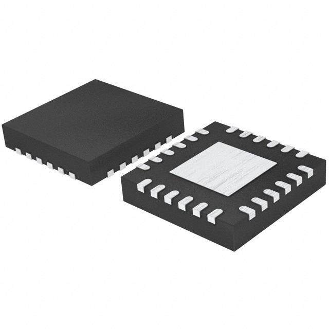
| 描述 | SENSOR IC MTRX TOUCH6KEY 28-QFN |
| 产品分类 | 电容式触摸传感器,接近传感器 IC |
| 品牌 | Atmel |
| 数据手册 | |
| 产品图片 |
|
| 产品型号 | AT42QT1060-MMU |
| PCN其它 | |
| rohs | 无铅 / 符合限制有害物质指令(RoHS)规范要求 |
| 产品系列 | QTouch™ |
| 产品培训模块 | http://www.digikey.cn/PTM/IndividualPTM.page?site=cn&lang=zhs&ptm=25037http://www.digikey.cn/PTM/IndividualPTM.page?site=cn&lang=zhs&ptm=25022 |
| 供应商器件封装 | 28-QFN(4x4) |
| 其它名称 | AT42QT1060-MMUQS397 |
| 分辨率(位) | 8 b |
| 包装 | 带卷 (TR) |
| 参考设计库 | http://www.digikey.com/rdl/4294959886/4294959868/848 |
| 安装类型 | 表面贴装 |
| 封装/外壳 | 28-VFQFN 裸露焊盘 |
| 工作温度 | -40°C ~ 85°C |
| 数据接口 | I²C |
| 数据速率/采样率(SPS,BPS) | 180k |
| 标准包装 | 6,000 |
| 电压-电源 | 1.8 V ~ 5.5 V |
| 电压基准 | 内部 |
| 电流-电源 | 10mA |
| 类型 | 电容式开关 |
| 触摸面板接口 | 6,2 线 |
| 评估工具 | 可供 |
| 输入/按键数 | 可配置,2 ~ 6 键 |
| 配用 | /product-detail/zh/EVK1060A/EVK1060A-ND/1982091 |


- 商务部:美国ITC正式对集成电路等产品启动337调查
- 曝三星4nm工艺存在良率问题 高通将骁龙8 Gen1或转产台积电
- 太阳诱电将投资9.5亿元在常州建新厂生产MLCC 预计2023年完工
- 英特尔发布欧洲新工厂建设计划 深化IDM 2.0 战略
- 台积电先进制程称霸业界 有大客户加持明年业绩稳了
- 达到5530亿美元!SIA预计今年全球半导体销售额将创下新高
- 英特尔拟将自动驾驶子公司Mobileye上市 估值或超500亿美元
- 三星加码芯片和SET,合并消费电子和移动部门,撤换高东真等 CEO
- 三星电子宣布重大人事变动 还合并消费电子和移动部门
- 海关总署:前11个月进口集成电路产品价值2.52万亿元 增长14.8%
PDF Datasheet 数据手册内容提取
Atmel AT42QT1060 Six-channel QTouch® Touch Sensor IC DATASHEET Features Configurations: Can be configured as a combination of keys and input/output lines Number of QTouch® Keys: Two to six Number of I/O Lines: Seven, configurable for input or output, with PWM control for LED driving Technology: Patented spread-spectrum charge-transfer (direct mode) Key Outline Sizes: 6mmx 6mm or larger (panel thickness dependent); widely different sizes and shapes possible Layers Required: One Electrode Materials: Etched copper Silver Carbon Indium Tin Oxide (ITO) Panel Materials: Plastic Glass Composites Painted surfaces (low particle density metallic paints possible) Panel Thickness: Up to 10mm glass (electrode size dependent) Up to 5mm plastic (electrode size dependent) Key Sensitivity: Individually settable via simple commands over serial interface Interface: I2C-compatible slave mode (100kHz). Discrete detection outputs Moisture Tolerance: Increased moisture tolerance based on hardware design and firmware tuning Signal Processing: Self-calibration auto drift compensation noise filtering Adjacent Key Suppression® (AKS®) Applications: Mobile appliances Power: 1.8V to 5.5V Package: 28-pin 4x4mm QFN RoHS compliant IC 9505H–AT42–04/2015
1. Pinout and Schematic 1.1 Pinout Configuration K 0 S 4 3 T L A G N O O S C D H S I I R S S C 28 27 26 25 24 23 22 SNS1K 1 21 IO2 SNS2K 2 20 IO1 VDD 3 19 IO0 VSS 4 QT1060 18 VSS IO5 5 17 VDD IO6 6 16 VDD SNS3K 7 15 SNS5 8 9 10 11 12 13 14 S4K S5K NS0 NS1 NS2 NS3 NS4 N N S S S S S S S 1.2 Pin Descriptions Table 1-1. Pin Allocation Pin Name Type Description If Unused, Connect To... 1 SNS1K I/O To Cs capacitor and to key Leave open 2 SNS2K I/O To Cs capacitor and to key Leave open 3 VDD P Positive power pin 4 VSS P Ground power pin 5 IO5 I/O I/O Port Pin 5 Leave open and set as output 6 IO6 I/O I/O Port Pin 6 Leave open and set as output 7 SNS3K I/O To Cs capacitor and to key Leave open 8 SNS4K I/O To Cs capacitor and to key Leave open 9 SNS5K I/O To Cs capacitor and to key Leave open 10 SNS0 I/O To Cs Capacitor Leave open 11 SNS1 I/O To Cs Capacitor Leave open 12 SNS2 I/O To Cs Capacitor Leave open 13 SNS3 I/O To Cs Capacitor Leave open AT42QT1060 [DATASHEET] 2 9505H–AT42–04/2015
Table 1-1. Pin Allocation (Continued) Pin Name Type Description If Unused, Connect To... 14 SNS4 I/O To Cs Capacitor Leave open 15 SNS5 I/O To Cs Capacitor Leave open 16 VDD P Positive power pin 17 VDD P Positive power pin 18 VSS P Ground power pin 19 IO0 I/O I/O Port Pin 0 Leave open and set as output 20 IO1 I/O I/O Port Pin 1 Leave open and set as output 21 IO2 I/O I/O Port Pin 2 Leave open and set as output 22 CHG OD Change line Leave open Resistor to Vdd or 23 SDA OD I2C Data line Vss only in standalone mode Resistor to Vdd or 24 SCL OD I2C Clock Line Vdd only in standalone mode 25 RST I Reset, active low Vdd 26 IO3 I/O I/O Port Pin 3 Leave open and set as output 27 IO4 I/O I/O Port Pin 4 Leave open and set as output 28 SNS0K I/O To Cs capacitor and to key Leave open I Input only O Output only, push-pull I/O Input/output OD Open drain output P Ground or power AT42QT1060 [DATASHEET] 3 9505H–AT42–04/2015
1.3 Schematic Figure 1-1. Typical Circuit Vunreg 100nF VDD Voltage Reg Note: Bypass capacitor to be tightly wired between Vdd and Vss. Followrecommendations from CB1 regulator manufacturer for input and output capacitors. 17 16 3 D D D D D D V V V Rs5 9 SNS5K KEY 5 25 RST SNS5 15 Cs5 Rs4 8 SNS4K KEY 4 6 IO6 SNS4 14 Cs4 Rs3 5 IO5 SNS3K 7 KEY 3 27 IO4 SNS3 13 Cs3 Rs2 IpOin sPort 26 IO3 SNS2K 2 KEY 2 21 IO2 SNS2 12 Cs2 20 Rs1 IO1 SNS1K 1 KEY 1 19 IO0 SNS1 11 Cs1 Rs0 SNS0K 28 KEY 0 SNS0 10 Cs0 Keep these parts QT1060 close to the IC VDD Rchg 100k SDA 23 I2C-compatible Data Change 22 CHG SCL 24 I2C-compatibleClock in Standalone Mode 23 S S SDA S S V V 18 4 VDD Note: The central pad on the underside of the chip is a 24 SCL Vss pin and should be connected to ground. Note: In some systems it may be desirable to connect RST to the master reset signal. For component values in Figure 1-1 check the following sections: • Section 3.1 on page 11: Cs capacitors (Cs0–Cs5) • Section 3.2 on page 11: Series resistors (Rs0–Rs5) • Section 3.5 on page 12: Voltage levels • Section 4.4 on page 15: SDA, SCL pull-up resistors (not shown) • Section 3.3 on page 11: LED traces AT42QT1060 [DATASHEET] 4 9505H–AT42–04/2015
Suggested regulator manufacturers: • Torex (XC6215 series) • Seiko (S817 series) • BCDSemi (AP2121 series) AT42QT1060 [DATASHEET] 5 9505H–AT42–04/2015
2. Overview 2.1 Introduction The AT42QT1060 (QT1060) is a digital burst mode charge-transfer (QT™) capacitive sensor driver designed specifically for mobile phone applications. The device can sense from two to six keys; up to four keys can be disabled by not installing their respective sense capacitors (Cs). It also has up to seven configurable input/output lines, with Pulse Width Modulation (PWM) for driving LEDs. This device includes all signal processing functions necessary to provide stable sensing under a wide variety of changing conditions, and the outputs are fully de-bounced. Only a few external parts are required for operation. The QT1060 modulates its bursts in a spread-spectrum fashion in order to heavily suppress the effects of external noise, and to suppress RF emissions. 2.2 Keys The QT1060 can have a minimum of two keys and a maximum of six keys. These can be constructed in different shapes and sizes. See “Features” on page 1 for the recommended dimensions. Unused keys should be disabled by removing the corresponding Cs and Rs components and connecting the SNS pins as shown in the If Unused column of Table on page 2. The unused keys are always pared from the burst sequence in order to optimize speed. See Section 6. on page 25 about setting up the keys. 2.3 Standalone Mode The QT1060 can operate in a standalone mode where an I2C-compatible interface is not required. To enter standalone mode, connect SDA to Vss and SCL to Vdd before powering up the QT1060. In standalone mode the default start-up values are used except for the I/O mask (Address 23). The I/O mask is configured so that all the I/Os are outputs (I/O mask=0x7F). This means that key detection is reported via the respective I/Os. 2.4 I/O Lines 2.4.1 Overview There is an input/output (I/O) port consisting of seven lines that can be individually programmed as inputs or outputs. They can be either a digital type or PWM. The PWM level can be set to 256 possible values and is common to all lines. The I/O lines are normally initialized as inputs. However, if an I2C interface is not used and the SDA and SCL pins are connected to Vss and Vdd respectively, then the I/O lines are initialized as outputs (see Section 2.3). The outputs can also be linked to either the detection channels or the output register to allow the outputs to be either user controlled or to indicate detection. These options can be set in the pin control masks (see Table on page 16). Unused I/O lines should be disabled by connecting as shown in the If Unused column of Table 1-1 on page 2. See Section 6. on page 25 about setting up the I/O lines. 2.4.2 I/O Mask A 1 in any bit position of this mask sets the corresponding pin to an output. If a bit is 0, the pin is an input and the function of the PWM, detect and active state masks will not matter for this pin. The level of the input pins is reflected in the input Status register. Changes to the logic levels on the inputs cause the CHG line to be asserted. AT42QT1060 [DATASHEET] 6 9505H–AT42–04/2015
2.4.3 PWM Mask A 1 in any bit position in this mask sets the corresponding pin to operate in PWM mode when its user output buffer is active and configured as an output. A zero sets the pin in digital mode. The PWM value is set in the PWM register that is writable via I2C communication. 2.4.4 Detection Mask A 1 in any bit position in this mask sets the corresponding pin to be controlled by the status register. If the pin is configured as an output, it is asserted automatically if there is a detection on the corresponding sensor channel. A zero in any bit sets the pin to be controlled by the user output buffer, allowing the user to control the pins directly. 2.4.5 Active Level Mask A 1 in any bit position in this mask sets the corresponding pin to be active high if configured as an output. A zero sets the pin to be active low. 2.5 Acquisition/Low Power Modes (LP) There are several different acquisition modes. These are controlled via the Low Power (LP) mode byte (see Section 5.12 on page 20) which can be written to via I2C communication. LP mode controls the intervals between acquisition measurements. Longer intervals consume lower power but have increased response time. During calibration and during the detect integrator (DI) period, the LP mode is temporarily set to LP mode 1 for a faster response. The QT1060 operation is based on a fixed cycle time of approximately 16ms. The LP mode setting indicates how many of these periods exist per measurement cycle. For example, if LPmode = 1, there is an acquisition every cycle (16ms). If LP mode = 3, there is an acquisition every 3 cycles (48ms), and so on. SLEEP mode (LP mode = 0) is available for minimum current drain. In this mode, the device is inactive, with the device status being held as it was before going to sleep, and no measurements are carried out. LP settings above mode 32 (512 ms) result in slower thermal drift compensation and should be avoided in applications where fast thermal transients occur. If LP mode=255 the device operates in Free-run mode. In this mode the device will not enter LP mode between measurements. The device continuously performs measurements one after another, resulting in the fastest response time but the highest power consumption. 2.6 Adjacent Key Suppression (AKS) Technology The device includes the Atmel-patented Adjacent Key Suppression technology, to allow the use of tightly spaced keys on a keypad with no loss of selectability by the user. There can be one AKS group, implemented so that only one key in the group may be reported as being touched at any one time. A key with a higher delta signal dominates and pushes a key with a smaller delta out of detect. This allows a user to slide a finger across multiple keys with only the dominant key reporting touch. The keys which are members of the AKS group can be set via the AKS mask (see Section 5.15 on page 21). Keys outside the group may be in detect simultaneously. For maximum flexibility there is no automatic key recalibration timeout on key detection. The user should issue a recalibration command if the key has been in detect for too long, for example for more than 30 seconds (see Figure 2.10). AT42QT1060 [DATASHEET] 7 9505H–AT42–04/2015
2.7 Change Line The Change line (see CHG in Figure 1-1 on page 4) signals when there is a change in state in the Detection or Input status bytes and is active low. It is cleared (allowed to float high) when the host reads the status bytes. If the status bytes change back to their original state before the host has read the status bytes (for example, a touch followed by a release), the CHG line will be held low. In this case, a read to any memory location will clear the CHG line. The CHG line is open-drain and should be connected via a 100k resistor to Vdd. It is necessary for minimum power operation as it ensures that the QT1060 can sleep for as long as possible. Communications wake up the QT1060 from sleep causing a higher power consumption if the part is randomly polled. The keys enabled by the key bit mask or a change in the Input port status cause a key change interrupt (see Table 5- 1 on page 16). Create a guard channel by removing that key from the key mask and including it in the AKS mask. Touching the guard channel does not cause an interrupt. The key and AKS masks are set by using the mask commands (see Table 5-1). 2.8 Types of Reset 2.8.1 External Reset An external reset logic line can be used if desired, fed into the RST pin. However, under most conditions it is acceptable to tie RST to Vdd. 2.8.2 Soft Reset The host can cause a device reset by writing a nonzero value to the reset byte. This soft reset triggers the internal watchdog timer on a ~16ms interval. After ~16ms the device resets and wakes again. After a further 30ms initialization period the device begins responding to its I2C slave address. After another ~80ms the device asserts the CHG line to indicate it is ready for touch sensing. The device NACKs any attempts to communicate with it during the first 30ms of its initialization period. After CHG goes low, the device calibrates the sensing channels. When complete, the CHG pin is set low once again. 2.9 Moisture Tolerance The presence of water (condensation, sweat, spilt water, and so on) on a sensor can alter the signal values measured and thereby affect the performance of any capacitive device. The moisture tolerance of QTouch devices can be improved by designing the hardware and fine-tuning the firmware following the recommendations in the application note Atmel AVR3002: Moisture Tolerant QTouch Design (www.atmel.com/Images/doc42017.pdf). 2.10 Calibration The command byte can force a recalibration at any time by writing a nonzero value to the calibration byte. This can be useful to clear out a stuck key condition after a prolonged period of uninterrupted detection. When the device recalibrates, it also autosenses which keys are enabled by examining the burst length of each electrode. If the burst length is either too short (if there is a missing or open Cs capacitor) or too long (a Cs capacitor is shorted), the key is ignored until the next calibration. The count of the number of currently enabled keys is found in the status response byte. This number can change after a CAL command; for example, if a Cs capacitor is intermittent. AT42QT1060 [DATASHEET] 8 9505H–AT42–04/2015
2.11 Guard Channel The device has a guard channel option, which allows any key, or combination of keys, to be configured as a guard channel to help prevent false detection. Guard channel keys should be more sensitive than the other keys (physically bigger or larger Cs), subject to burst length limitations (see Section 2.12.3). With guard channel enabled, the designated key(s) is connected to a sensor pad which detects the presence of touch and overrides any output from the other keys using the chip AKS feature. The guard channel option is enabled by an I2C command. To enable a guard channel the relevant key should be removed from the key mask (see Table 5-1 on page 16). In addition, the guard channel needs to be included within the AKS mask with the other keys for the guard function to operate. Note that a detection on the guard channel does not cause a change request. With the guard channel not enabled, all the keys work normally. Figure 2-1. Guard Channel Example Guardchannel 2.12 Signal Processing 2.12.1 Detect Threshold The device detects a touch when the signal has crossed a threshold level and remained there for a specified number of counts (see Section 5.11 on page 19). This can be altered on a key-by-key basis using the key threshold I2C commands. 2.12.2 Detect Integrator The device features a fast detection integrator counter (DI filter), which acts to filter out noise at the small expense of slower response time. The DI filter requires a programmable number of consecutive samples confirmed in detection before the key is declared to be touched. There is also a fast DI on the end of the detection (see Section 5.20 on page 23). The fast DI will not be applied at the start of a detection if a detection on any other channel has already been declared. 2.12.3 Burst Length Limitations In a balanced system common signals are regarded as thermal shifts and are removed by the relative referencing drifting, if enabled. This means that the burst lengths must be similar. This can be checked by reading the reference values (Address 52–63) and making sure that they are similar. The absolute maximum difference is that the maximum value of reference is less than three times the minimum value amongst all the channels. It is recommended having the burst lengths (references) as close together as possible, through better routing and layout. For example, if the keys have references of 250, 230, 220, 240, 200 and 210, this is acceptable. If the keys have references of 250, 230, 220, 240, 200 and 710, the efficiency of the relative referencing drifting will be affected. The last key’s (710) layout should be changed or relative referencing be disabled. The closer the references are in value, the better the relative referencing drifting performs. AT42QT1060 [DATASHEET] 9 9505H–AT42–04/2015
If only normal drifting is enabled, the burst lengths can have bigger variations. The normal operating limit of burst lengths is between 16 and 1536 counts. A value out of these limits causes the respective key to be disabled and not measured until a calibration. Signal value for an out-of-limit key is zero. AT42QT1060 [DATASHEET] 10 9505H–AT42–04/2015
3. Wiring and Parts 3.1 Cs Sample Capacitors Cs0–Cs5 are the charge sensing sample capacitors; normally they are identical in nominal value. The optimal Cs values depend on the thickness of the panel and its dielectric constant. Thicker panels require larger values of Cs. Typical values are 2.2nF to 10nF. The value of Cs should be chosen so that a light touch on a key produces a reduction of ~10–20 in the key signal value (see Section 5.22 on page 23). The chosen Cs value should never be so large that the key signals exceed ~1000, as reported by the chip in the debug data. The Cs capacitors must be X7R or PPS film type, for stability. For consistent sensitivity, they should have a 10%tolerance. A 20% tolerance may cause small differences in sensitivity from key to key and unit to unit. If a channel is not used, the Cs capacitor may be omitted. 3.2 Rs Resistors Series resistors Rs (Rs0–Rs5) are inline with the electrode connections and should be used to limit electrostatic discharge (ESD) currents and to suppress radio frequency (RF) interference. They should be approximately 4.7k to 20k each. Although these resistors may be omitted, the device may become susceptible to external noise or radio frequency interference (RFI). For details of how to select these resistors see the Application Note QTAN0002, Secrets of a Successful QTouch Design, downloadable from the Touch Technology area of the Atmel website, www.atmel.com. 3.3 LED Traces and Other Switching Signals Digital switching signals near the sense lines induce transients into the acquired signals, deteriorating the SNR performance of the device. Such signals should be routed away from the sensing traces and electrodes, or the design should be such that these lines are not switched during the course of signal acquisition (bursts). LED terminals which are multiplexed or switched into a floating state, and which are within, or physically very near, a key (even if on another nearby PCB) should be bypassed to either Vss or Vdd with at least a 10nF capacitor. This is to suppress capacitive coupling effects which can induce false signal shifts. The bypass capacitor does not need to be next to the LED, in fact it can be quite distant. The bypass capacitor is noncritical and can be of any type. LED terminals which are constantly connected to Vss or Vdd do not need further bypassing. 3.4 PCB Cleanliness Modern no-cleanflux is generally compatible with capacitive sensing circuits. CAUTION: If a PCB is reworked to correct soldering faults relating to the device, or to any associated traces or components, be sure that you fully understand the nature of the flux used during the rework process. Leakage currents from hygroscopic ionic residues can stop capacitive sensors from functioning. If you have any doubts, a thorough cleaning after rework may be the only safe option. If a PCB is reworked in any way, clean it thoroughly to remove all traces of the flux residue around the capacitive sensor components. Dry it thoroughly before any further testing is conducted. AT42QT1060 [DATASHEET] 11 9505H–AT42–04/2015
3.5 Power Supply See Section 7.2 on page 26 for the power supply range. If the power supply fluctuates slowly with temperature, the device tracks and compensates for these changes automatically with only minor changes in sensitivity. If the supply voltage drifts or shifts quickly, the drift compensation mechanism is not able to keep up, causing sensitivity anomalies or false detections. The usual power supply considerations with QT parts apply to the device. The power should be clean and come from a separate regulator if possible. However, this device is designed to minimize the effects of unstable power, and except in extreme conditions should not require a separate Low Dropout (LDO) regulator. See underneath Figure 1-1 on page 4 for suggested regulator manufacturers. Caution: A regulator IC shared with other logic can result in erratic operation and is not advised. A single ceramic 0.1µF bypass capacitor, with short traces, should be placed very close to the power pins of the IC. Failure to do so can result in device oscillation, high current consumption, erratic operation, and so on. It is assumed that a larger bypass capacitor (~1µF) is somewhere else in the power circuit; for example, near the regulator. To assist with transient regulator stability problems, the QT1060 waits 500µs any time it wakes up from a sleep state (that is, in SLEEP and LP modes) before acquiring, to allow Vdd to fully stabilize. 3.6 Bus Specification Table 3-1. I2C Bus Specification Parameter Unit Address space 7-bit Maximum bus speed (SCL) 100kHz Hold time START condition 4µs minimum Setup time for STOP condition 4µs minimum Bus free time between a STOP and START condition 4.7µs minimum Rise times on SDA and SCL 1µs maximum AT42QT1060 [DATASHEET] 12 9505H–AT42–04/2015
4. I2C Communications 4.1 I2C Protocol 4.1.1 Protocol The I2C protocol is based around access to an address table (see Table 5-1 on page 16) and supports multibyte reads and writes. The maximum clock rate is 100kHz. 4.1.2 Signals The I2C interface requires two signals to operate: SDA - Serial Data SCL - Serial Clock A third line, CHG, is used to signal when the device has seen a change in the status byte: CHG: Open-drain, active low when any capacitive key in the key mask has changed state or any input line has changed state since the last I2C read. After reading the two status bytes, this pin floats (high) again if it is pulled up with an external resistor. If the status bytes change back to their original state before the host has read the status bytes (for example, a touch followed by a release), the CHG line will be held low. In this case, a read to any memory location will clear the CHG line. 4.1.3 Clock Stretching The device has an internal monitor that resets its I2C hardware if either I2C-compatible line is held low, without the other line changing, for more than about 14ms. It is important that no other device on the bus clock stretches for 14ms, otherwise the monitor will reset the I2C hardware and transfers with the chip may be corrupted. If the device is configured to run in stand-alone mode, the monitor will be turned off. 4.2 I2C Address There is one preset I2C address of 0x12. This is not changeable. AT42QT1060 [DATASHEET] 13 9505H–AT42–04/2015
4.3 Data Read/Write 4.3.1 Writing Data to the Device The sequence of events required to write data to the device is shown next Host to Device DeviceTx to Host S SLA+W A MemAddress A Data A P . Table 4-1. Description of Write Data Bits Key Description S Start condition SLA+W Slave address plus write bit A Acknowledge bit MemAddress Target memory address within device Data Data to be written P Stop condition 1. The host initiates the transfer by sending the START condition 2. The host follows this by sending the slave address of the device together with the WRITE bit. 3. The device sends an ACK. 4. The host then sends the memory address within the device it wishes to write to. 5. The device sends an ACK. 6. The host transmits one or more data bytes; each is acknowledged by the device. 7. If the host sends more than one data byte, they are written to consecutive memory addresses. 8. The device automatically increments the target memory address after writing each data byte. 9. After writing the last data byte, the host should send the STOP condition. Note: the host should not try to write beyond address 255 because this is the limit of the device’s internal memory address. 4.3.2 Reading Data From the Device The sequence of events required to read data from the device is shown next. Host to Device DeviceTx to Host S SLA+W A MemAddress A P S SLA+R A Data 1 A Data 2 A Data n A P 1. The host initiates the transfer by sending the START condition 2. The host follows this by sending the slave address of the device together with the WRITE bit. 3. The device sends an ACK. 4. The host then sends the memory address within the device it wishes to read from. 5. The device sends an ACK. AT42QT1060 [DATASHEET] 14 9505H–AT42–04/2015
6. The host must then send a STOP and a START condition followed by the slave address again but this time accompanied by the READ bit. 7. The device returns an ACK, followed by a data byte. 8. The host must return either an ACK or NACK. 1. If the host returns an ACK, the device subsequently transmits the data byte from the next address. Each time a data byte is transmitted, the device automatically increments the internal address. The device continues to return data bytes until the host responds with a NACK. 2. If the host returns a NACK, it should then terminate the transfer by issuing the STOP condition. 9. The device resets the internal address to the location indicated by the memory address sent to it previously. Therefore, there is no need to send the memory address again when reading from the same location. 4.4 SDA, SCL The I2C bus transmits data and clock with SDA and SCL respectively. They are open-drain; that is I2C master and slave devices can only drive these lines low or leave them open. The termination resistors (not shown) pull the line up to Vdd if no I2C-compatible device is pulling it down. The termination resistors commonly range from 1k to 10k and should be chosen so that the rise times on SDA and SCL meet the I2C specifications (1µs maximum). Standalone mode: if I2C-compatible communications are not required, then standalone mode can be enabled by connecting SDA to Vss and SCL to Vdd. See Section 2.3 on page 6 for more information. AT42QT1060 [DATASHEET] 15 9505H–AT42–04/2015
5. Setups 5.1 Introduction The device calibrates and processes signals using a number of algorithms specifically designed to provide for high survivability in the face of adverse environmental challenges. User-defined Setups are employed to alter these algorithms to suit each application. These Setups are loaded into the device over the I2C serial interfaces. Table 5-1. Internal Register Address Allocation Address Use R/W Bit 7 Bit 6 Bit 5 Bit 4 Bit 3 Bit 2 Bit 1 Bit 0 0 Chip ID R Major ID (=3) Minor ID (=1) 1 Version R Device version number 2 Minor version R Minor version number 3 Reserved Reserved 4 Detection status R Calibrating Res Key5 Key4 Key3 Key2 Key1 Key0 5 Input port status R Res Input 6 Input 5 Input 4 Input 3 Input 2 Input 1 Input 0 6–11 Reserved Reserved 12 Calibrate R/W Writing a nonzero value forces a calibration 13 Reset R/W Writing a nonzero value forces a reset 14 Drift Option R/W Res Res Res Res Res Res Res DRIFT Positive 15 R/W MSB LSB Recalibration Delay 16 NTHR key 0 R/W MSB LSB 17 NTHR key 1 R/W MSB LSB 18 NTHR key 2 R/W MSB LSB 19 NTHR key 3 R/W MSB LSB 20 NTHR key 4 R/W MSB LSB 21 NTHR key 5 R/W MSB LSB 22 LP mode R/W MSB LSB 23 I/O mask R/W MSB IO6 IO5 IO4 IO3 IO2 IO1 IO0 24 Key mask R/W CAL Res Key 5 Key 4 Key 3 Key 2 Key 1 Key 0 25 AKS mask R/W Res Res Key 5 Key 4 Key 3 Key 2 Key 1 Key 0 26 PWM mask R/W Res IO6 IO5 IO4 IO3 IO2 IO1 IO0 27 Detection mask R/W Res IO6 IO5 IO4 IO3 IO2 IO1 IO0 28 Active level mask R/W Res IO6 IO5 IO4 IO3 IO2 IO1 IO0 29 User output buffer R/W Res IO6 IO5 IO4 IO3 IO2 IO1 IO0 30 DI R/W MSB LSB 31 PWM level R/W MSB LSB AT42QT1060 [DATASHEET] 16 9505H–AT42–04/2015
Table 5-1. Internal Register Address Allocation (Continued) Address Use R/W Bit 7 Bit 6 Bit 5 Bit 4 Bit 3 Bit 2 Bit 1 Bit 0 32–39 Reserved Reserved 40–51 Key 0–5 Signal R 52–63 Key 0–5 Reference R Note: Res = Reserved; only write zero to these bits. 5.2 Address 0: Chip ID Table 5-2. Chip ID Address b7 b6 b5 b4 b3 b2 b1 b0 0 MAJOR ID MINOR ID MAJOR ID: Reads back as 3 MINOR ID: Reads back as 1 5.3 Address 1: Device Version Number Table 5-3. Device Version Number Address b7 b6 b5 b4 b3 b2 b1 b0 1 DEVICE VERSION NUMBER DEVICE VERSION NUMBER: this is the 8-bit firmware version number (0x03). 5.4 Address 2: Minor Version Number Table 5-4. Minor Version Number Address b7 b6 b5 b4 b3 b2 b1 b0 2 MINOR VERSION NUMBER MINOR VERSION NUMBER: this is the 8-bit minor firmware revision number (0x00). AT42QT1060 [DATASHEET] 17 9505H–AT42–04/2015
5.5 Address 4: Detection Status Table 5-5. Detection Status Address b7 b6 b5 b4 b3 b2 b1 b0 4 CAL Reserved KEY5 KEY4 KEY3 KEY2 KEY1 KEY0 CAL: a 1 indicates that the QT1060 is currently calibrating. KEY0–5: bits 0 to 5 indicate which keys are in detection, if any; touched keys report as 1, untouched or disabled keys report as 0. 5.6 Address 5: Input Port Status Table 5-6. Input Port Status Address b7 b6 b5 b4 b3 b2 b1 b0 5 Reserved INPUT 6 INPUT 5 INPUT 4 INPUT 3 INPUT 2 INPUT 1 INPUT 0 INPUT 0–6: these bits indicate the state of the I/O lines that are configured as inputs; 1indicating logic 1 on the input, 0 indicating logic 0. The bits corresponding to any keys configured as outputs read as 0. 5.7 Address 12: Calibrate Table 5-7. Calibrate Address b7 b6 b5 b4 b3 b2 b1 b0 12 Writing a nonzero value forces a calibration Writing any nonzero value into this address triggers the device to start a calibration cycle. The CAL flag in the status register is set when begun and cleared when the calibration has finished. 5.8 Address 13: Reset Table 5-8. Reset Address b7 b6 b5 b4 b3 b2 b1 b0 13 Writing a nonzero value forces a reset Writing any nonzero value to this address triggers the device to reset. AT42QT1060 [DATASHEET] 18 9505H–AT42–04/2015
5.9 Address 14: Drift Option Table 5-9. Drift Option Address b7 b6 b5 b4 b3 b2 b1 b0 14 Reserved DRIFT DRIFT: there are two types of drift option: normal and relative referencing. If DRIFT = 0, relative referencing and normal drift are enabled. If DRIFT = 1, only normal drift is enabled. Relative referencing compensates for fast signal drifts that are common to all keys. This mode is suitable if the keys are placed close to each other and have closely matched burst lengths (see Section 2.12.3 on page 9). Normal drifting is also carried out but at a slower rate compared to the relative referencing drift rate. Default: 1 (relative referencing Off) 5.10 Address 15: Positive Recalibration Delay Table 5-10. Positive Recalibration Delay Address b7 b6 b5 b4 b3 b2 b1 b0 15 POSITIVE RECALIBRATION DELAY POSITIVE RECALIBRATION DELAY: If any key is found to have a significant drop in capacitance, that is, an “away from touch” signal, then this is deemed to be an error condition. If this condition persists for more than the Positive Recalibration Delay (PRD) period, then an automatic recalibration is carried out on all keys. The condition that the error is triggered on depends on the drift compensation mode. If relative referencing drifting is enabled (DRIFT = 0), then an “away from touch” delta of more than four counts triggers the error. If only normal mode drifting is enabled (DRIFT = 1), then an “away from touch” delta of more than 75% of the NTHR triggers the error. In LP mode the Positive Recalibration Delay is the PRD value multiplied by 16ms cycle time; in Free Run Mode the Positive Recalibration delay is the PRD value multiplied by the minimum cycle time (~7ms, but depends on Cs and design). Default: 40 (40×16ms = 640ms; default LP is 32ms) 5.11 Address 16 – 21: NTHR Keys 0 – 5 Table 5-11. NTHR Keys 0 – 5 Address b7 b6 b5 b4 b3 b2 b1 b0 16–21 MSB LSB NTHR Keys 0–5: these 8-bit values set the threshold value for each key to register a detection. Default: 10 counts AT42QT1060 [DATASHEET] 19 9505H–AT42–04/2015
5.12 Address 22: LP Mode Table 5-12. LP Mode Address b7 b6 b5 b4 b3 b2 b1 b0 22 MSB LSB LP Mode: this 8-bit value determines the number of 16ms intervals between key measurements. Longer intervals between measurements yield lower power consumption at the expense of slower response to touch. LP7–0 Mode 0 SLEEP 1 16ms 2 32ms 3 48ms 4 64ms ... ... 254 4.064 s 255 Free-run A value of zero causes the device to enter SLEEP mode where no measurements are performed. A value of 255 causes the device to enter Free-run mode where measurements are continuously performed without entering a low power mode between measurements. This provides the fastest response time but also the highest power consumption. Default: 2 (32ms between key acquisitions) 5.13 Address 23: I/O Mask Table 5-13. I/O Mask Address b7 b6 b5 b4 b3 b2 b1 b0 23 Reserved IO6 IO5 IO4 IO3 IO2 IO1 IO0 IO0–IO6: these bits control the direction of the I/O pins. A 1 sets the pin as an output, a 0 as an input. See Section 5.24 on page 24 for I/O register precedence and example usage. Default: 0 (all I/Os are set as inputs, when using the I2C-compatible mode) (all I/Os are set as outputs (0x7F), when using the standalone mode) AT42QT1060 [DATASHEET] 20 9505H–AT42–04/2015
5.14 Address 24: Key Mask Table 5-14. Key Mask Address b7 b6 b5 b4 b3 b2 b1 b0 24 CAL Reserved KEY5 KEY4 KEY3 KEY2 KEY1 KEY0 CAL: this bit controls whether the CAL bit causes a CHG transition. KEY0–5 (Key Mask): these bits control whether a change in the corresponding bit in the detection status register generates a transition on the CHG line. A 1 allows the status bit to cause a CHG request, a 0 stops the corresponding bit from causing a CHG request. Default: 0xBF (all bits create a CHG request) 5.15 Address 25: AKS Mask Table 5-15. AKS Mask Address b7 b6 b5 b4 b3 b2 b1 b0 25 Reserved Reserved KEY5 KEY4 KEY3 KEY2 KEY1 KEY0 KEY0–5 (AKS Mask): these bits control which keys are included in the AKS group. A 1 means the corresponding key is included in the AKS group and may only go into detect when it has the largest signal change of any key in the group. A 0 means that it is excluded and can go into detect whenever its threshold is passed. Default: 0x00 (no keys are within the AKS group) 5.16 Address 26: PWM Mask Table 5-16. PWM Mask Address b7 b6 b5 b4 b3 b2 b1 b0 26 Reserved I/O6 I/O5 I/O4 I/O3 I/O2 I/O1 I/O0 I/O0–6 (PWM Mask): these bits control which I/Os that are configured as outputs, and its user output buffer activated, will output a PWM signal. A 1 means the output generates a PWM signal, a 0 means the output generates a logic level. The active level of the output (both logical and PWM) is determined by the Active level mask. See Section 5.24 on page 24 for I/O register precedence and example usage. Default: 0x00 (PWM is off on all I/Os) AT42QT1060 [DATASHEET] 21 9505H–AT42–04/2015
5.17 Address 27: Detection Mask Table 5-17. Detection Mask Address b7 b6 b5 b4 b3 b2 b1 b0 27 Reserved I/O6 I/O5 I/O4 I/O3 I/O2 I/O1 I/O0 I/O0–6 (Detection Mask): these bits control which I/Os that are configured as outputs will be controlled by their corresponding capacitive key. A 1 means the output n generates an active output when key n is detecting a touch. A 0 means that the output is controlled by the output buffer. See Section 5.24 on page 24 for I/O register precedence and example usage. Default: 0x3F (all I/Os are controlled by key status) 5.18 Address 28: Active Level Mask Table 5-18. Active Level Mask Address b7 b6 b5 b4 b3 b2 b1 b0 28 Reserved I/O6 I/O5 I/O4 I/O3 I/O2 I/O1 I/O0 I/O0–6 (Active Level Mask): these bits control the active logic level for the I/Os that are configured as outputs. A 1 means the output generates an active high output, a 0 means that the output is active low. See Section 5.24 for I/O register precedence and example usage. Default: 0 (all I/Os are active low output) 5.19 Address 29: User Output Buffer Table 5-19. User Output Buffer Address b7 b6 b5 b4 b3 b2 b1 b0 29 Reserved I/O6 I/O5 I/O4 I/O3 I/O2 I/O1 I/O0 I/O0–6 (User Output Buffer): these bits control the output level for the I/Os that are configured as outputs. A 1 means the output generates an active output, a 0 means that the output is inactive. See Section 5.24 on page 24 for I/O register precedence and example usage. Default: 0 (all I/Os inactive) AT42QT1060 [DATASHEET] 22 9505H–AT42–04/2015
5.20 Address 30: Detection Integrator Table 5-20. Detection Integrator Address b7 b6 b5 b4 b3 b2 b1 b0 30 MSB DETECTION INTEGRATOR LSB DETECTION INTEGRATOR: this 8-bit value controls the number of consecutive measurements that must be confirmed as having passed the key threshold before that key is registered as being in detect. A value of zero should not be used. Default: 3 5.21 Address 31: PWM Level Table 5-21. PWM Level Address b7 b6 b5 b4 b3 b2 b1 b0 31 MSB PWM LEVEL LSB PWM LEVEL: this 8-bit value controls the duty cycle of the PWM output signal. Valid values are between 0...255. There is a constant level band at either end of the range, so: A value of 0...10 gives a 100% low output A value of 250...255 gives a 100% high output Default: 128 (50:50 duty cycle) 5.22 Address 40 – 51: Key Signal Table 5-22. Key Signal Address b7 b6 b5 b4 b3 b2 b1 b0 40 LSB OF KEY SIGNAL FOR KEY 0 41 MSB OF KEY SIGNAL FOR KEY 0 42–51 LSB/MSB OF KEY SIGNAL FOR KEYS 1–5 KEY SIGNAL: addresses 40–51 allow key signals to be read for each key, starting with key 0. There are two bytes of data for each key. These are the key’s 16-bit key signals which are accessed as two 8-bit bytes, stored LSB first. These addresses are read-only. AT42QT1060 [DATASHEET] 23 9505H–AT42–04/2015
5.23 Address 52–63: Reference Data Table 5-23. Reference Data Address b7 b6 b5 b4 b3 b2 b1 b0 52 LSB OF REFERENCE DATA FOR KEY 0 53 MSB OF REFERENCE DATA FOR KEY 0 54–63 LSB/MSB OF REFERENCE DATA FOR KEYS 1–5 REFERENCE DATA: addresses 52–63 allow reference data to be read for each key, starting with key 0. There are two bytes of data for each key. These are the key’s 16-bit reference data which is accessed as two 8-bit bytes, stored LSB first. These addresses are read-only. 5.24 Mask Precedence Table 5-24 gives the order of priority for the settings in the mask inputs/outputs. The settings in the left-most column have the highest priority, those in the second-left have the next priority, and so on. If two or more settings are incompatible then the setting in the left-hand column overrides the other. The right-most column, I/O Function, specifies the expected result. Table 5-24. Input/Output Mask Precedence I/O Mask Detection PWM Mask Active Level User Reg QTouch Key I/O Function (bit n) Mask (bit n) (bit n) Mask (bit n) (bit n) (channel n) (I/O n) 0 X X X X X Digital Input 1 0 0 0 0 X Output - Vdd 1 0 0 0 1 X Output - 0V 1 0 0 1 0 X Output - 0V 1 0 0 1 1 X Output - Vdd 1 0 1 0 0 X Output - Vdd 1 0 1 0 1 X PWM Output 1 0 1 1 0 X Output - 0V 1 0 1 1 1 X PWM Output 1 1 0 0 X Untouched Output - Vdd 1 1 0 0 X Touched Output - 0V 1 1 0 1 X Untouched Output - 0V 1 1 0 1 X Touched Output - Vdd 1 1 1 0 X Untouched Output - Vdd 1 1 1 0 X Touched PWM Output 1 1 1 1 X Untouched Output - 0V 1 1 1 1 X Touched PWM Output Note: X = don’t care (can be a 1 or a 0) AT42QT1060 [DATASHEET] 24 9505H–AT42–04/2015
6. Setting Up Procedures To Set Up Keys To Set Up I/O Lines Determine the direction of the I/O Set the number of keys required by lines.If any lines are unused, set leaving the SNS pins unconnected in them to be outputs and leave them unused keys. unconnected. [Address 23: I/O Mask] Determine whether a change in the corresponding bit in the detection status register generates a transition Determine which I/Os that are on the CHG line. configured as outputs will be controlled by their corresponding [Address 24: Key Mask] capacitive key. [Address 27: Detection Mask] Determine which keys are in the AKS group. Determine the duty cycle of the PWM [Address 25: AKS Mask] output signal. [Address 31: PWM Level] Determine the number of measurements that must be confirmed as having passed the key Determine which I/Os that are threshold before that key is registered configured as outputs will output a as being in detect. PWM signal. [Address 30: Detection Integrator] [Address 26: PWM Mask] Tune the sensitivity of the keys by Determine the active logic level for the adjusting the value of the sampling I/Os that are configured as outputs. capacitor, Cs and the negative threshold (NTHR) [Address 28: Active Level Mask] [Address 16 –21: NTHR] Determine the output level for the I/Os that are configured as outputs. [Address 29: User Output Buffer] AT42QT1060 [DATASHEET] 25 9505H–AT42–04/2015
7. Specifications 7.1 Absolute Maximum Specifications Vdd –0.5 to +6 V Max continuous pin current, any control or drive pin ±10mA Short circuit duration to ground, any pin infinite Short circuit duration to Vdd, any pin infinite Voltage forced onto any pin –0.6V to (Vdd + 0.6) V CAUTION: Stresses beyond those listed under Absolute Maximum Specifications may cause permanent damage to the device. This is a stress rating only and functional operation of the device at these or other conditions beyond those indicated in the operational sections of this specification is not implied. Exposure to absolute maximum specification conditions for extended periods may affect device reliability. 7.2 Recommended Operating Conditions Operating temp –40oC to +85oC Storage temp –55oC to +125oC Vdd +1.8 V to 5.5 V Supply ripple+noise ±25mV Cx load capacitance per key 2 – 20pF 7.3 DC Specifications Vdd = 3.3 V, Cs = 10 nF, load = 5 pF, 32 ms default sleep, Ta = recommended range, unless otherwise noted Parameter Description Minimum Typical Maximum Units Notes Vil Low input logic level – – 0.2×Vdd V Vih High input logic level 0.6×Vdd – – V Vol Low output voltage – – 0.5 V 4mA sink Voh High output voltage Vdd – 0.7V – – V 1mA source Iil Input leakage current – – ±1 µA Ar Acquisition resolution – 8 – bits AT42QT1060 [DATASHEET] 26 9505H–AT42–04/2015
7.4 Current Consumption Cs = 10nF, Cx = 5 pF, Rs = 10k Idd (µA) at Vdd = LP Mode 5V 3.3V 1.8V 0 (SLEEP) 2.48 1.8 1.1 1 (16ms) 1745 1135 403 2 (32ms) 1615 1065 373 4 (64ms) 1545 1030 360 8 (128ms) 1510 1010 351 16 (256ms) 1500 1000 348 32 (512ms) 1485 995 346 64 (1024ms) 1475 992 345 7.5 Timing Specifications Parameter Description Minimum Typical Maximum Units Notes LP mode + T Response time DI setting×16ms – ms Under host control R (DIsetting×16ms) Modulated spread- F Sample frequency 162 180 198 kHz QT spectrum (chirp) Power-up delay to Can be longer if T operate/calibration – <230 – ms D burst is very long. time F I2C clock rate – – 100 kHz – I2C Fm Burst modulation, – ±8 – % – Reset pulse width 5 – – µs – Clock stretch – 25 40 µs – AT42QT1060 [DATASHEET] 27 9505H–AT42–04/2015
7.6 Mechanical Dimensions Note: The central pad on the underside of the QFN chip should be connected to ground. Do not run any tracks underneath the body of the chip, only ground. (cid:17) (cid:6) (cid:5) (cid:2) (cid:10)(cid:20)(cid:21)(cid:16)(cid:5)(cid:16)*(cid:17) Z $ %*(cid:17)$(cid:16)(cid:9)*$x F(cid:5) #"(cid:10)(cid:16)(cid:9)*$x (cid:16)F ^ ‘ (cid:17)(cid:2) G(cid:31)\Q (cid:17)(cid:10)(cid:18)(cid:18)(cid:10)(cid:7)(cid:9)(cid:2)(cid:6)(cid:18)(cid:12)(cid:7)(cid:19)(cid:6)(cid:10)(cid:7)(cid:19) (cid:5) =>(cid:21)(cid:20)(cid:23)(cid:16)(cid:22)?(cid:16)(cid:4)(cid:15)(cid:11)(cid:27)<(cid:18)(cid:15)(cid:16)@(cid:16)(cid:29)(cid:29)E (cid:2) Y(cid:16)G(cid:31)(cid:2)G (cid:19)(cid:20)(cid:18)(cid:21)(cid:10)(cid:15) (cid:18)(cid:6)(cid:7) (cid:7)(cid:10)(cid:18) (cid:18)(cid:4)(cid:22) (cid:7)(cid:10)(cid:14)(cid:12) Z (cid:16)F(cid:16) G(cid:31)(cid:3)G(cid:16) G(cid:31)JG(cid:16) (cid:5)(cid:31)GG(cid:16) $(cid:2) (cid:16)F(cid:5)(cid:16) G(cid:31)GG(cid:16) G(cid:31)G(cid:2)(cid:16) G(cid:31)GQ(cid:16) (cid:16)V(cid:16) G(cid:31)(cid:5)X(cid:16) G(cid:31)(cid:2)(cid:2)(cid:16) G(cid:31)(cid:2)X V (cid:16)(cid:6)(cid:16) (cid:16) G(cid:31)(cid:2)G(cid:16)Y$;(cid:16) (cid:16)(cid:17)(cid:16) Z(cid:31)JQ(cid:16) \(cid:31)GG(cid:16) \(cid:31)GQ (cid:16)(cid:17)(cid:2)(cid:16) (cid:2)(cid:31)ZQ(cid:16) (cid:2)(cid:31)\G(cid:16) (cid:2)(cid:31)\Q + (cid:16)$(cid:16) Z(cid:31)JQ(cid:16) \(cid:31)GG(cid:16) \(cid:31)GQ (cid:15) (cid:16)$(cid:2)(cid:16) (cid:2)(cid:31)ZQ(cid:16) (cid:2)(cid:31)\G(cid:16) (cid:2)(cid:31)\Q G(cid:31)\(cid:16)Y(cid:15)? (cid:16)(cid:15)(cid:16) (cid:16) G(cid:31)\Q =\zE (cid:8)"##"(cid:4)(cid:16)(cid:9)*$x (cid:16)+(cid:16) G(cid:31)ZQ(cid:16) G(cid:31)\G(cid:16) G(cid:31)\Q (cid:16)^(cid:16) G(cid:31)GG(cid:16) _(cid:16) G(cid:31)G(cid:3) !"#$%(cid:24)(cid:16)(cid:16)#&(cid:15)(cid:16)(cid:23)(cid:15)(cid:18)(cid:29)(cid:20)(cid:21)(cid:11)(cid:30)(cid:16)’(cid:5)(cid:16)*(cid:17)(cid:16)(cid:20)(cid:27)(cid:16)(cid:11)(cid:16)+(cid:11)(cid:27)(cid:15)(cid:18)-(cid:29)(cid:11)(cid:18)(cid:13)(cid:15)(cid:26)(cid:16);(cid:15)(cid:11)(cid:23)<(cid:18)(cid:15)(cid:31) (cid:16)‘(cid:16) G(cid:31)(cid:2)G(cid:16) _(cid:16) _ (cid:2)(cid:3)(cid:2)(cid:4)(cid:3)(cid:2)(cid:5) (cid:14)(cid:6)(cid:14)(cid:15)(cid:12) (cid:8)(cid:16)(cid:17) (cid:2)(cid:3)(cid:4)(cid:5)(cid:6)(cid:7)(cid:8)(cid:9)(cid:7)(cid:10)(cid:11) (cid:3)(cid:12)(cid:13)(cid:11)(cid:9)(cid:9) (cid:23)(cid:24)(cid:18)(cid:25){(cid:16)(cid:2)(cid:3)-(cid:25)(cid:11)(cid:26){(cid:16)\(cid:16)z(cid:16)\(cid:16)z(cid:16)(cid:5)(cid:31)G(cid:16)(cid:29)(cid:29)(cid:16)(cid:8)(cid:22)(cid:26)^{(cid:16)(cid:16)(cid:16)+(cid:15)(cid:11)(cid:26)(cid:16)(cid:10)(cid:20)(cid:23)(cid:12)&(cid:16)G(cid:31)\Q(cid:16)(cid:29)(cid:29){(cid:16) (cid:10)(cid:11)(cid:12)(cid:13)(cid:11)(cid:14)(cid:15)(cid:16)(cid:17)(cid:18)(cid:11)(cid:19)(cid:20)(cid:21)(cid:14)(cid:16)(cid:6)(cid:22)(cid:21)(cid:23)(cid:11)(cid:12)(cid:23)(cid:24) (cid:2)(cid:31)\(cid:16)z(cid:16)(cid:2)(cid:31)\(cid:16)(cid:29)(cid:29)(cid:16)$z(cid:25)(cid:22)(cid:27)(cid:15)(cid:26)(cid:16)(cid:10)(cid:11)(cid:26){(cid:16)(cid:16)#&(cid:15)(cid:18)(cid:29)(cid:11)(cid:30)(cid:30)^(cid:16)$(cid:21)&(cid:11)(cid:21)(cid:12)(cid:15)(cid:26)(cid:16) (cid:7)(cid:8)(cid:9) (cid:2)(cid:3)(cid:4)(cid:5) (cid:6) (cid:25)(cid:11)(cid:12)(cid:13)(cid:11)(cid:14)(cid:15)(cid:26)(cid:18)(cid:11)(cid:19)(cid:20)(cid:21)(cid:14)(cid:27)(cid:28)(cid:11)(cid:23)(cid:29)(cid:15)(cid:30)(cid:31)(cid:12)(cid:22)(cid:29) (cid:10)(cid:30)(cid:11)(cid:27)(cid:23)(cid:20)(cid:12)(cid:16)(cid:9)(cid:15)(cid:18)^(cid:16)#&(cid:20)(cid:21)(cid:16)|<(cid:11)(cid:26)(cid:16);(cid:30)(cid:11)(cid:23)(cid:16)!(cid:22)(cid:16)+(cid:15)(cid:11)(cid:26)(cid:16)(cid:10)(cid:11)(cid:12)(cid:13)(cid:11)(cid:14)(cid:15)(cid:16)=(cid:9)|;!E(cid:16) AT42QT1060 [DATASHEET] 28 9505H–AT42–04/2015
7.7 Marking There are two possible types of chip marking. 28 Pin1ID ChipTraceability 1 LTCODE Code 1060 Abbreviationof Part number; AT42QT1060-MMU AT Programweekcodenumber1-52where: A=1,B=2...Z=26 thenusingtheunderscore A=27...Z=52 28 Pin1ID 1 AT42 QT1060 Partnumber; AT42QT1060-MMU -MMU LTCODE Chip Traceability Code AT42QT1060 [DATASHEET] 29 9505H–AT42–04/2015
7.8 Part Number Part Number Description AT42QT1060-MMU 28-pin 4x4mm QFN RoHS compliant IC The part number comprises: AT = Atmel 42 = Touch Business Unit QT = Charge-transfer technology 1060 = (1) Keys (06) number of channels (0) variant number MMU = Package identifier 7.9 Moisture Sensitivity Level (MSL) MSL Rating Peak Body Temperature Specifications MSL1 260oC IPC/JEDEC J-STD-020 AT42QT1060 [DATASHEET] 30 9505H–AT42–04/2015
Appendix A. I2C Basics A.1 Interface Bus The device communicates with the host over an I2C bus. The following sections give an overview of the bus; more detailed information is available from www.i2C-bus.org. Devices are connected to the I2C bus as shown in Figure A- 1. Both bus lines are connected to Vdd via pull-up resistors. The bus drivers of all I2C devices must be open-drain type. This implements a wired AND function that allows any and all devices to drive the bus, one at a time. A low level on the bus is generated when a device outputs a zero. Figure A-1. I2C Interface Bus Vdd Device 1 Device 2 Device 3 Device n R1 R2 SDA SCL A.2 Transferring Data Bits Each data bit transferred on the bus is accompanied by a pulse on the clock line. The level of the data line must be stable when the clock line is high; the only exception to this rule is for generating START and STOP conditions. Figure A-2. Data Transfer SDA SCL Data Stable Data Stable Data Change AT42QT1060 [DATASHEET] 31 9505H–AT42–04/2015
A.3 START and STOP Conditions The host initiates and terminates a data transmission. The transmission is initiated when the host issues a START condition on the bus, and is terminated when the host issues a STOP condition. Between the START and STOP conditions, the bus is considered busy. As shown in Figure A-3, START and STOP conditions are signaled by changing the level of the SDA line when the SCL line is high. Figure A-3. START and STOP Conditions SDA SCL START STOP A.4 Address Byte Format All address bytes are 9 bits long, consisting of 7 address bits, one READ/WRITE control bit and an acknowledge bit. If the READ/WRITE bit is set, a read operation is performed, otherwise a write operation is performed. When the device recognizes that it is being addressed, it will acknowledge by pulling SDA low in the ninth SCL (ACK) cycle. An address byte consisting of a slave address and a READ or a WRITE bit is called SLA+R or SLA+W, respectively. The most significant bit of the address byte is transmitted first. The address sent by the host must be consistent with that selected with the option jumpers. Figure A-4. Address Byte Format Addr MSB Addr LSB R/W ACK SDA SCL 1 2 7 8 9 START AT42QT1060 [DATASHEET] 32 9505H–AT42–04/2015
A.5 Data Byte Format All data bytes are 9 bits long, consisting of 8 data bits and an acknowledge bit. During a data transfer, the host generates the clock and the START and STOP conditions, while the receiver is responsible for acknowledging the reception. An acknowledge (ACK) is signaled by the receiver pulling the SDA line low during the ninth SCL cycle. If the receiver leaves the SDA line high, a NACK is signaled. Figure A-5. Data Byte Format Data MSB Data LSB ACK Aggregate SDA SDA from Transmitter SDA from Receiver SCL from Master 1 2 7 8 9 SLA+R/W Data Byte Stop orNext Data Byte A.6 Combining Address and Data Bytes into a Transmission A transmission consists of a START condition, an SLA+R/W, one or more data bytes and a STOP condition. The wired ANDing of the SCL line is used to implement handshaking between the host and the device. The device extends the SCL low period by pulling the SCL line low whenever it needs extra time for processing between the data transmissions. Note: Each write or read cycle must end with a stop condition. The device may not respond correctly if a cycle is terminated by a new start condition. Figure A-6 shows a typical data transmission. Note that several data bytes can be transmitted between the SLA+R/W and the STOP. Figure A-6. Byte Transmission Addr MSB Addr LSB R/W ACK Data MSB Data LSB ACK SDA SCL 1 2 7 8 9 1 2 7 8 9 START SLA+RW Data Byte STOP A.7 AT42QT1060 [DATASHEET] 33 9505H–AT42–04/2015
Revision History Revision Number History Revision A – September 2008 Initial Release for code revision 3.0 Revision B – October 2008 Minor amendments to burst length limitations Revision C – November 2008 Minor amendments to improve clarity Revision D – December 2008 Chip ID updated Revision E – February 2009 Additional information on I2C interface added Revision F – November 2012 Updated PWM information and clock stretch timing added Revision G – May 2013 Applied new template Revision H – April 2015 Updated MSL value from 3 to 1 AT42QT1060 [DATASHEET] 34 9505H–AT42–04/2015
X X X X X X Atmel Corporation 1600 Technology Drive, San Jose, CA 95110 USA T: (+1)(408) 441.0311 F: (+1)(408) 436.4200 | www.atmel.com © 2015 Atmel Corporation. / Rev.: Atmel-9505H-AT42_04/2015. Atmel®, Atmel logo, Enabling Unlimited Possiblities® and combinations thereof, Adjacent Key Suppression®, AKS®, QTouch®,and others are registered trademarks or trademarks of Atmel Corporation or its subsidiaries. Other terms and product names may be trademarks of others. DISCLAIMER: The information in this document is provided in connection with Atmel products. No license, express or implied, by estoppel or otherwise, to any intellectual property right is granted by this document or in connection with the sale of Atmel products. EXCEPT AS SET FORTH IN THE ATMEL TERMS AND CONDITIONS OF SALES LOCATED ON THE ATMEL WEBSITE, ATMEL ASSUMES NO LIABILITY WHATSOEVER AND DISCLAIMS ANY EXPRESS, IMPLIED OR STATUTORY WARRANTY RELATING TO ITS PRODUCTS INCLUDING, BUT NOT LIMITED TO, THE IMPLIED WARRANTY OF MERCHANTABILITY, FITNESS FOR A PARTICULAR PURPOSE, OR NON-INFRINGEMENT. IN NO EVENT SHALL ATMEL BE LIABLE FOR ANY DIRECT, INDIRECT, CONSEQUENTIAL, PUNITIVE, SPECIAL OR INCIDENTAL DAMAGES (INCLUDING, WITHOUT LIMITATION, DAMAGES FOR LOSS AND PROFITS, BUSINESS INTERRUPTION, OR LOSS OF INFORMATION) ARISING OUT OF THE USE OR INABILITY TO USE THIS DOCUMENT, EVEN IF ATMEL HAS BEEN ADVISED OF THE POSSIBILITY OF SUCH DAMAGES. Atmel makes no representations or warranties with respect to the accuracy or completeness of the contents of this document and reserves the right to make changes to specifications and products descriptions at any time without notice. Atmel does not make any commitment to update the information contained herein. Unless specifically provided otherwise, Atmel products are not suitable for, and shall not be used in, automotive applications. Atmel products are not intended, authorized, or warranted for use as components in applications intended to support or sustain life. SAFETY-CRITICAL, MILITARY, AND AUTOMOTIVE APPLICATIONS DISCLAIMER: Atmel products are not designed for and will not be used in connection with any applications where the failure of such products would reasonably be expected to result in significant personal injury or death (“Safety-Critical Applications”) without an Atmel officer's specific written consent. Safety-Critical Applications include, without limitation, life support devices and systems, equipment or systems for the operation of nuclear facilities and weapons systems. Atmel products are not designed nor intended for use in military or aerospace applications or environments unless specifically designated by Atmel as military-grade. Atmel products are not designed nor intended for use in automotive applications unless specifically designated by Atmel as automotive-grade.
Mouser Electronics Authorized Distributor Click to View Pricing, Inventory, Delivery & Lifecycle Information: M icrochip: AT42QT1060-MMU AT42QT1060-MMUR
/AT42QT1060-MMU.jpg)
 Datasheet下载

