ICGOO在线商城 > 集成电路(IC) > 嵌入式 - FPGA(现场可编程门阵列) > AT40K10-2AQC
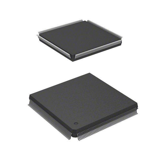
.jpg|http://media.digikey.com/Renders/Cypress%20Semi%20Renders/100TQFP.jpg)
 Datasheet下载
- 型号: AT40K10-2AQC
- 制造商: Atmel
- 库位|库存: xxxx|xxxx
- 要求:
| 数量阶梯 | 香港交货 | 国内含税 |
| +xxxx | $xxxx | ¥xxxx |
查看当月历史价格
查看今年历史价格
AT40K10-2AQC产品简介:
ICGOO电子元器件商城为您提供AT40K10-2AQC由Atmel设计生产,在icgoo商城现货销售,并且可以通过原厂、代理商等渠道进行代购。 AT40K10-2AQC价格参考。AtmelAT40K10-2AQC封装/规格:嵌入式 - FPGA(现场可编程门阵列), 。您可以下载AT40K10-2AQC参考资料、Datasheet数据手册功能说明书,资料中有AT40K10-2AQC 详细功能的应用电路图电压和使用方法及教程。
| 参数 | 数值 |
| 产品目录 | 集成电路 (IC) |
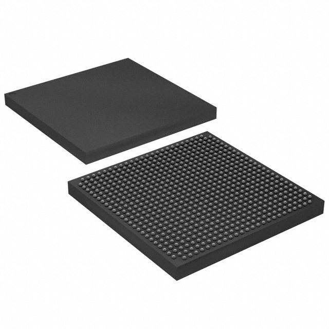
| 描述 | IC FPGA 78 I/O 100TQFP |
| 产品分类 | |
| I/O数 | 78 |
| LAB/CLB数 | - |
| 品牌 | Atmel |
| 数据手册 | |
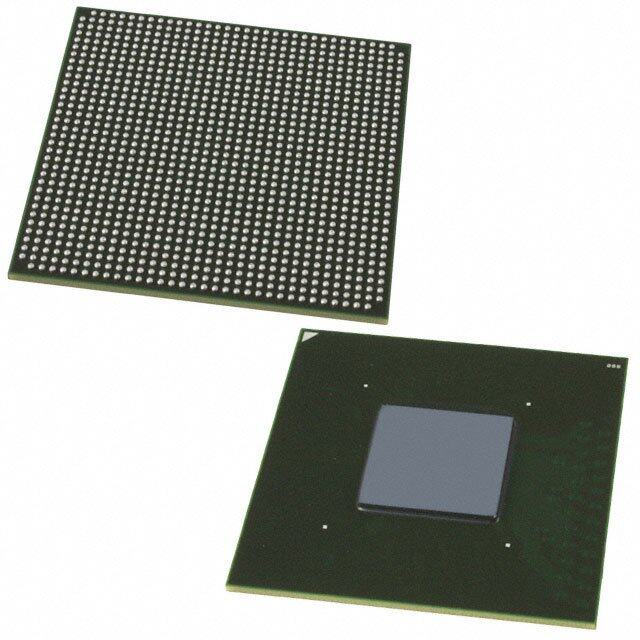
| 产品图片 |
|
| 产品型号 | AT40K10-2AQC |
| rohs | 含铅 / 不符合限制有害物质指令(RoHS)规范要求 |
| 产品系列 | AT40K/KLV |
| 产品目录页面 | |
| 供应商器件封装 | 100-TQFP(14x14) |
| 其它名称 | AT40K102AQC |
| 安装类型 | 表面贴装 |
| 封装/外壳 | 100-TQFP |
| 工作温度 | 0°C ~ 70°C |
| 总RAM位数 | 4608 |
| 栅极数 | 20000 |
| 标准包装 | 90 |
| 电压-电源 | 4.75 V ~ 5.25 V |
| 逻辑元件/单元数 | 576 |

.jpg)


- 商务部:美国ITC正式对集成电路等产品启动337调查
- 曝三星4nm工艺存在良率问题 高通将骁龙8 Gen1或转产台积电
- 太阳诱电将投资9.5亿元在常州建新厂生产MLCC 预计2023年完工
- 英特尔发布欧洲新工厂建设计划 深化IDM 2.0 战略
- 台积电先进制程称霸业界 有大客户加持明年业绩稳了
- 达到5530亿美元!SIA预计今年全球半导体销售额将创下新高
- 英特尔拟将自动驾驶子公司Mobileye上市 估值或超500亿美元
- 三星加码芯片和SET,合并消费电子和移动部门,撤换高东真等 CEO
- 三星电子宣布重大人事变动 还合并消费电子和移动部门
- 海关总署:前11个月进口集成电路产品价值2.52万亿元 增长14.8%


PDF Datasheet 数据手册内容提取
Features • UltraHighPerformance – SystemSpeedsto100MHz – ArrayMultipliers>50MHz – 10nsFlexibleSRAM – InternalTri-stateCapabilityinEachCell (cid:127) FreeRAM™ – Flexible,Single/DualPort,Synchronous/Asynchronous10nsSRAM – 2,048-18,432BitsofDistributedSRAMIndependentofLogicCells (cid:127) 128-384PCICompliantI/Os 5K - 50K Gates – 3V/5VCapability – ProgrammableOutputDrive – Fast,FlexibleArrayAccessFacilitatesPinLocking Coprocessor – Pin-compatiblewithXC4000,XC5200FPGAs (cid:127) 8GlobalClocks FPGA with – Fast,LowSkewClockDistribution – ProgrammableRising/FallingEdgeTransitions FreeRAM™ – DistributedClockShutdownCapabilityforLowPowerManagement – GlobalReset/AsynchronousResetOptions – 4AdditionalDedicatedPCIClocks (cid:127) CacheLogic®DynamicFull/PartialRe-configurabilityIn-System AT40K05 – UnlimitedRe-programmabilityviaSerialorParallelModes – EnablesAdaptiveDesigns AT40K05LV – EnablesFastVectorMultiplierUpdates – QuickChange™ToolsforFast,EasyDesignChanges AT40K10 (cid:127) Pin-compatiblePackageOptions – PlasticLeadedChipCarriers(PLCC) – Thin,PlasticQuadFlatPacks(LQFP,TQFP,PQFP) AT40K10LV – BallGridArrays(BGAs) (cid:127) Industry-standardDesignTools AT40K20 – SeamlessIntegration(Libraries,Interface,FullBack-annotation)with Concept®,Everest,Exemplar™,Mentor®,OrCAD®,Synario™,Synopsys®, AT40K20LV Verilog®,Veribest®,Viewlogic®,Synplicity® – TimingDrivenPlacement&Routing AT40K40 – Automatic/InteractiveMulti-chipPartitioning – Fast,EfficientSynthesis AT40K40LV – Over75AutomaticComponentGeneratorsCreate1000s ofReusable,FullyDeterministicLogicandRAMFunctions (cid:127) IntellectualPropertyCores – FirFilters,UARTs,PCI,FFTandOtherSystemLevelFunctions (cid:127) EasyMigrationtoAtmelGateArraysforHighVolumeProduction (cid:127) SupplyVoltage5VforAT40K,and3.3VforAT40KLV Rev.0896C–FPGA–04/02 1
Table1. AT40K/AT40KLV Family(1) AT40K05 AT40K10 AT40K20 AT40K40 Device AT40K05LV AT40K10LV AT40K20LV AT40K40LV UsableGates 5K-10K 10K-20K 20K-30K 40K-50K RowsxColumns 16x16 24x24 32x32 48x48 Cells 256 576 1,024 2,304 Registers 256(1) 576(1) 1,024(1) 2,304(1) RAMBits 2,048 4,608 8,192 18,432 I/O(Maximum) 128 192 256 384 Note: 1. PackageswithFCKwillhave8lessregisters. Description The AT40K/AT40KLV is a family of fully PCI-compliant, SRAM-based FPGAswith dis- tributed 10ns programmable synchronous/asynchronous, dual-port/single-port SRAM, 8globalclocks,CacheLogicability(partiallyorfullyreconfigurablewithoutlossofdata), automaticcomponentgenerators, andrange insize from 5,000 to 50,000usablegates. I/O counts range from 128 to 384 in industry standard packages ranging from 84-pin PLCCto352-ballSquareBGA,andsupport5VdesignsforAT40K and3.3Vdesignsfor AT40KLV. The AT40K/AT40KLV is designed to quickly implement high-performance, large gate countdesignsthroughtheuseof synthesisandschematic-basedtoolsusedonaPCor Sun platform. Atmel’s design tools provide seamless integration with industry standard tools suchasSynplicity,ModelSim,ExemplarandViewlogic. The AT40K/AT40KLV can be used as a coprocessor for high-speed (DSP/processor- based)designsbyimplementingavarietyofcomputationintensive,arithmeticfunctions. These include adaptive finite impulse response (FIR) filters, fast Fourier transforms (FFT), convolvers, interpolators and discrete-cosine transforms (DCT) that are required for video compression and decompression, encryption, convolution and other multime- diaapplications. Fast, Flexible and TheAT40K/AT40KLV FPGAoffersapatenteddistributed10nsSRAM capabilitywhere Efficient SRAM theRAMcanbeusedwithoutlosinglogicresources.Multipleindependent,synchronous or asynchronous, dual-port or single-port RAM functions (FIFO, scratch pad, etc.) can becreatedusingAtmel’smacrogeneratortool. Fast, Efficient Array and The AT40K/AT40KLV’s patented 8-sided core cell with direct horizontal, vertical and Vector Multipliers diagonal cell-to-cell connections implements ultra fast array multipliers without using any busing resources. The AT40K/AT40KLV’s Cache Logic capability enables a large number of design coefficients and variables to be implemented in a very small amount of silicon,enablingvastimprovement in systemspeedat much lowercost thanconven- tionalFPGAs. AT40K/AT40KLV Series FPGA 2 0896C–FPGA–04/02
AT40K/AT40KLV Series FPGA Cache Logic Design The AT40K/AT40KLV, AT6000 and FPSLIC families are capable of implementing Cache Logic (dynamic full/partial logic reconfiguration, without loss of data, on-the-fly) forbuildingadaptivelogicandsystems.Asnewlogicfunctionsarerequired,theycanbe loadedintothelogiccachewithoutlosingthedataalreadythereordisruptingtheopera- tion of the rest of the chip; replacing or complementing the active logic. The AT40K/AT40KLVcanactasareconfigurablecoprocessor. Automatic Component The AT40K/AT40KLV FPGA family is capable of implementing user-defined, automati- Generators cally generated, macros in multiple designs; speed and functionality are unaffected by themacroorientationordensityofthetargetdevice.Thisenablesthefastest,mostpre- dictable and efficient FPGA design approach and minimizes design risk by reusing already proven functions. The Automatic Component Generators work seamlessly with industry standard schematic and synthesis tools to create the fastest, most efficient designsavailable. The patented AT40K/AT40KLV series architecture employs a symmetrical grid of small yet powerful cells connected to a flexible busing network. Independently controlled clocksandresetsgoverneverycolumnofcells.Thearrayissurroundedbyprogramma- bleI/O. Devicesrange in size from 5,000 to 50,000usable gates in the family, and have 256 to 2,304 registers. Pin locations are consistent throughout the AT40K/AT40KLV seriesfor easy design migration in the same package footprint. The AT40K/AT40KLV series FPGAs utilize a reliable 0.6µ single-poly, CMOS process and are 100% factory-tested. Atmel’sPC-andworkstation-basedintegrateddevelopmentsystem(IDS)isusedtocre- ateAT40K/AT40KLVseriesdesigns.Multipledesignentrymethods aresupported. The Atmel architecture was developed to provide the highest levels of performance, functional density and design flexibility in an FPGA. The cells in the Atmel array are small, efficient and can implement any pair of Boolean functions of (the same) three inputsoranysingleBooleanfunctionof fourinputs.Thecell’ssmallsizeleadstoarrays with large numbers of cells, greatly multiplying the functionality in each cell. A simple, high-speed busing network provides fast, efficient communication over medium and longdistances. 3 0896C–FPGA–04/02
The Symmetrical At the heart of the Atmel architecture is a symmetrical array of identical cells, Array see Figure1.Thearrayiscontinuousfromoneedgetotheother,exceptforbusrepeat- ersspacedeveryfourcells,seeFigure2onpage5.Attheintersectionofeachrepeater row and column there is a 32x4 RAM block accessible by adjacent buses. The RAM can be configured as either a single-ported or dual-ported RAM(1), with either synchro- nousorasynchronousoperation. Note: 1. Theright-mostcolumncanonlybeusedassingle-portRAM. Figure1. SymmetricalArraySurroundedbyI/O(AT40K20) = I/O Pad = Repeater Row = FreeRAM = AT40K Cell = Repeater Column AT40K/AT40KLV Series FPGA 4 0896C–FPGA–04/02
AT40K/AT40KLV Series FPGA Figure2. FloorPlan(RepresentativePortion)(1) RV = Vertical Repeater = Horizontal Repeater RH = Core Cell RAM RV RV RV RV RAM RV RV RV RV RAM RV RV RV RV RAM RH RH RH RH RH RH RH RH RH RH RH RH RH RH RH RH RAM RV RV RV RV RAM RV RV RV RV RAM RV RV RV RV RAM RH RH RH RH RH RH RH RH RH RH RH RH RH RH RH RH RAM RV RV RV RV RAM RV RV RV RV RAM RV RV RV RV RAM RH RH RH RH RH RH RH RH RH RH RH RH RH RH RH RH RAM RV RV RV RV RAM RV RV RV RV RAM RV RV RV RV RAM Note: 1. Repeaters regenerate signals and can connect any bus to any other bus (all path- ways are legal) on the same plane. Each repeater has connections to two adjacent local-bussegmentsandtwoexpress-bussegments.Thisisdoneautomaticallyusing theintegrateddevelopmentsystem(IDS)tool. 5 0896C–FPGA–04/02
The Busing Network Figure3onpage7depictsoneoffiveidenticalbusingplanes.Eachplanehasthreebus resources: a local-bus resource (the middle bus) and two express-bus (both sides) resources. Bus resources are connected via repeaters. Each repeater hasconnections to two adjacent local-bus segments and two express-bus segments. Each local-bus segment spans four cells and connects to consecutive repeaters. Each express-bus segment spans eight cells and “leapfrogs”orbypasses a repeater. Repeaters regener- ate signals and can connect any bus to any other bus (all pathways are legal) on the same plane. Although not shown, a local bus can bypass a repeater via a programma- ble pass gate allowing long on-chip tri-state buses to be created. Local/Local turns are implemented through pass gates in the cell-bus interface. Express/Express turns are implementedthroughseparatepassgates distributedthroughoutthearray. Some of the bus resources on the AT40K/AT40KLV are used as a dual-function resources.Table2showswhichbusesareusedinadual-functionmodeandwhichbus planeisused.TheAT40K/AT40KLV softwaretoolsaredesignedtoaccommodatedual- functionbusesinanefficientmanner. Table2. Dual-functionBuses Function Type Plane(s) Direction Comments CellOutputEnable Local 5 Horizontal andVertical RAMOutputEnable Express 2 Vertical Busfulllengthatarrayedge Businfirstcolumntoleftof RAMblock RAMWriteEnable Express 1 Vertical Busfulllengthatarrayedge Businfirstcolumntoleftof RAMblock RAMAddress Express 1-5 Vertical Busesfulllengthatarrayedge Busesinsecondcolumntoleft ofRAMblock RAMDataIn Local 1 Horizontal DataInconnectstolocal busplane1 RAMDataOut Local 2 Horizontal Dataoutconnectstolocal busplane2 Clocking Express 4 Vertical Bushalflengthatarrayedge Set/Reset Express 5 Vertical Bushalflengthatarrayedge AT40K/AT40KLV Series FPGA 6 0896C–FPGA–04/02
AT40K/AT40KLV Series FPGA Figure3. BusingPlane(OneofFive) = AT40K/AT40KLV Core Cell = Local/Local or Express/Express Turn Point = Row Repeater = Column Repeater Express Express Bus Bus Local Bus 7 0896C–FPGA–04/02
Cell Connections Figure 4(a) depicts direct connections between a cell and its eight nearest neighbors. Figure 4(b)showstheconnectionsbetweena cellandfivehorizontal local buses(1per busingplane)andfiveverticallocalbuses (1perbusingplane). Figure4. CellConnections 54321 e e e e e CELL CELL CELL nnnnn aaaaa PlPlPlPlPl Plane 5 PPPPllllaaaannnneeee 4321 HBuosriiznogn Ptalalne WXYZL CELL CELL CELL WXYZL CELL Diagonal Vertical Direct Connect Busing Plane CELL CELL CELL Orthogonal Direct Connect (a) Cell-to-cell Connections (b) Cell-to-bus Connections The Cell Figure 5 depicts the AT40K/AT40KLV cell. Configuration bits for separate muxes and pass gates are independent. All permutations of programmable muxes and pass gates are legal. V (V -V ) is connected to the vertical local bus in plane n. H (H -H ) is n 1 5 n 1 5 connectedtothehorizontallocalbusinplanen. Alocal/localturninplanenisachieved by turning onthe two passgates connectedto V and H . Pass gates areopened to let n n signals into the cell from a local bus or to drive a signal out onto a local bus. Signals cominginto thelogiccellononelocal busplane canbeswitchedontoanotherplaneby opening two of the pass gates. This allows bus signals to switch planes to achieve greaterrouteability.Uptofivesimultaneouslocal/localturns arepossible. The AT40K/AT40KLV FPGA core cellisa highlyconfigurable logicblockbased around two 3-input LUTs (8 x 1 ROM), which can be combined to produce one 4-input LUT. Thismeansthatanycorecellcanimplementtwofunctions of3inputsoronefunctionof 4 inputs. There is a Set/Reset D flip-flop in every cell, the output of which may be tri- stated and fed back internally within the core cell. There is also a 2-to-1 multiplexer in everycell,andanupstream ANDgateinthe“frontend”of the cell. ThisANDgateisan importantfeatureintheimplementationofefficientarraymultipliers. With this functionality in each core cell, the core cell can be configured in several “modes”. The core cell flexibility makes the AT40K/AT40KLV architecture well suited to mostdigitaldesignapplicationareas,seeFigure6. AT40K/AT40KLV Series FPGA 8 0896C–FPGA–04/02
AT40K/AT40KLV Series FPGA Figure5. TheCell "1" NW NE SE SW "1" "1" N E S W X W Y Z X W Y FB 8X1 LUT 8X1 LUT OUT OUT "1" "0" "1" V1 V2 V3 V4 V5 H1 H2 H3 H4 H5 Pass gates 1 0 Z "1" OEHOEV L D CLOCK Q RESET/SET X Y NW NE SE SW N E S W X = Diagonal Direct Connect or Bus Y = Orthogonal Direct Connect or Bus W = Bus Connection Z = Bus Connection FB = Internal Feedback 9 0896C–FPGA–04/02
Figure6. SomeSingleCellModes Synthesis Mode. This mode is particularly important for A the use of VHDL/Verilog design. VHDL/Verilog Synthesis CB UT DQ Q (Registered) tools generally will produce as their output large amounts L and/or D of random logic functions. Having a 4-input LUT structure Q gives efficient random logic optimization without the delays associated with larger LUT structures. The output of any cell may be registered, tri-stated and/or fed back into a core cell. SUM Arithmetic Mode is frequently used in many designs. UT or Acasn c iamnp bleem seenetn a i n1 -tbhiet ffuigllu ared,d tehre ( 2A-Tin4p0uKt/ AaTd4d0eKr wLVit hc obroet hc ell L Carry In and Carry Out) in one core cell. Note that the A DQ SUM (Registered) B sum output in this diagram is registered. This output could C and/or then be tri-stated and/or fed back into the cell. UT CARRY L DSP/Multiplier Mode. This mode is used to efficiently UT DQ PRODUCT (Registered) implement array multipliers. An array multiplier is an array A L or of bitwise multipliers, each implemented as a full adder B PRODUCT with an upstream AND gate. Using this AND gate and the C diagonal interconnects between cells, the array multiplier D and/or structure fits very well into the AT40K/AT40KLV T U CARRY architecture. L Counter Mode. Counters are fundamental to almost all digital designs. They are the basis of state machines, timing chains and clock dividers. A counter is essentially T U DQ Q an increment by one function (i.e., an adder), with the L input being an output (or a decode of an output) from the CARRY IN and/or previous stage. A 1-bit counter can be implemented in one core cell. Again, the output can be registered, tri-stated and/or fed back. T U CARRY L Tri-state/Mux Mode. This mode is used in many X A U telecommunications applications, where data needs to be B M Q routed through more than one possible path. The output of C 1 2: the core cell is very often tri-statable for many inputs to many outputs data switching. EN AT40K/AT40KLV Series FPGA 10 0896C–FPGA–04/02
AT40K/AT40KLV Series FPGA RAM 32x4dual-portedRAMblocksaredispersedthroughoutthearray,seeFigure7.A4-bit Input Data Bus connects to fourhorizontallocal busesdistributed over foursectorrows (plane 1). A 4-bit Output Data Bus connects to four horizontal local buses distributed overfoursectorsinthesamecolumn.A5-bitOutputAddressBusconnectstofiveverti- cal express buses in the same column. Ain (input address) and Aout (output address) alternate positions in horizontally aligned RAM blocks. For the left-most RAM blocks, Aout is on the left and Ain is on the right. For the right-most RAM blocks, Ain is on the left andAoutistiedoff,thusitcanonlybeconfiguredasasingleport.Forsingle-ported RAM, Ain is the READ/WRITE address port and Din is the (bi-directional) data port. Right-most RAM blocks can be used only for single-ported memories. WEN and OEN connecttotheverticalexpressbusesinthesamecolumn. Figure7. RAMConnections(OneRamBlock) CLK CLK CLK CLK Din Dout Ain Aout 32 x 4 RAM WEN OEN CLK 11 0896C–FPGA–04/02
Reading and writing of the 10ns 32x4 dual-port FreeRAM are independent of each other. Reading the 32 x4 dual-port RAM is completely asynchronous. Latches are transparent; when Load is logic 1, data flows through; when Load is logic 0, data is latched. These latches are used to synchronize Write Address, Write Enable Not, and DinsignalsforasynchronousRAM.Eachbitinthe32x4dual-portRAMisalsoatrans- parent latch. The front-endlatch and the memorylatchtogether form an edge-triggered flip flop. When a nibble (bit= 7) is (Write) addressed and LOAD is logic 1 and WE is logic 0, data flows through the bit. When a nibble is not (Write) addressed or LOAD is logic 0 orWE is logic 1, data is latched in the nibble. The two CLOCK muxes are con- trolled together; they both select CLOCK (for a synchronous RAM) or they both select “1”(foranasynchronousRAM).CLOCKisobtainedfromtheclockforthesector-column immediately to the left and immediately above the RAM block. Writing any value to the RAM clear byte during configuration clears the RAM (see the “AT40KConfiguration Series”applicationnoteatwww.atmel.com). Figure8. RAMLogic CLOCK “1” “1” 0 1 1 0 Load 5 Ain Read Address 5 Load Aout Latch Write Address 32 x 4 Dual-port RAM “1”OE Load WEN Latch Write Enable NOT 4 Load 4 Din Latch Din Dout Dout Clear RAM-Clear Byte Figure 9 on page 13 shows an example of a RAM macro constructed using the AT40K/AT40KLV’s FreeRAM cells. The macro shown is a 128 x8 dual-ported asyn- chronous RAM. Note the very small amount of external logic required to complete the addressdecoding forthe macro. Most of the logic cells (core cells)in the sectors occu- pied by the RAM will be unused: they can be used for other logic in the design. This logic canbeautomaticallygeneratedusingthemacrogenerators. AT40K/AT40KLV Series FPGA 12 0896C–FPGA–04/02
0 8 9 6 C – F P G A – 0 4 /0 2 F ig u r e 9 . WE R A 2-to-4 M Write Decoder E Address x a m 2-to-4 Read p Decoder Address le : 1 2 8 A Din(0) Dout(0) x 8 T Din(1) Dout(1) D 4 u Din(2) Dout(2) al-p 0K Din(3) Dout(3) o rte /A Din Dout Din Dout Din Dout Din Dout d Ain Aout Aout Ain Ain Aout Aout Ain R T WEN WEN WEN WEN AM 4 OEN OEN OEN OEN 0 ( Din(4) Dout(4) A K s Din(5) Dout(5) yn L ch V Din(6) Dout(6) r o n S Din(7) Dout(7) o u e s Din Dout Din Dout Din Dout Din Dout ) r Ain Aout Aout Ain Ain Aout Aout Ain Local Buses ie WEN WEN WEN WEN Express Buses s OEN OEN OEN OEN Dedicated Connections F P G 1 A 3
Clocking Scheme There are eight Global Clock buses (GCK1 - GCK8) on the AT40K/AT40KLV FPGA. EachoftheeightdedicatedGlobalClockbusesisconnectedtooneofthedual-useGlo- bal Clock pins. Any clocks used in the design should use global clocks where possible: this canbedone by usingAssign Pin Locks to lockthe clockstothe Global Clock loca- tions. In addition to the eight Global Clocks, there arefour Fast Clocks (FCK1 - FCK4), twoperedgecolumnofthearrayforPCIspecification. Eachcolumnofanarrayhasa“ColumnClockmux”anda“SectorClockmux”.TheCol- umnClockmuxisatthetopof everycolumn ofanarrayand theSectorClockmuxisat every four cells. The Column Clock muxis selected from one of the eight Global Clock buses. The clock provided to each sector column of four cells isinverted, non-inverted or tied off to “0”, using the Sector Clock mux to minimize the power consumption in a sectorthathasnoclocks.TheclockcaneithercomefromtheColumnClockorfromthe Plane4 express bus, see Figure10onpage 15. The extreme-left Column Clock mux hastwoadditionalinputs,FCK1andFCK2,toprovidefastclockingtoleft-sideI/Os.The extreme-right ColumnClockmuxhastwoadditional inputsas well, FCK3and FCK4, to providefastclockingtoright-sideI/Os. Theregisterineachcellistriggeredonarisingclockedgebydefault.Beforeconfigura- tion on power-up, constant “0” is provided to each register’s clock pins. After configuration on power-up, the registers either set or reset, depending on the user’s choice. The clocking scheme is designed to allow efficient use of multiple clocks with low clock skew,bothwithinacolumnandacrossthecorecellarray. AT40K/AT40KLV Series FPGA 14 0896C–FPGA–04/02
AT40K/AT40KLV Series FPGA Figure10. Clocking(forOneColumnofCells) } FCK (2 per Edge Column of the Array) GCK1 - GCK8 Column Clock Mux “1” Sector Clock Mux Global Clock Line (Buried) Express Bus (Plane 4; Half Length at Edge) “1” Repeater Sector Clock Mux “1” “1” 15 0896C–FPGA–04/02
Set/Reset Scheme The AT40K/AT40KLV familyreset scheme isessentiallythe same asthe clockscheme except that there is only one Global Reset. A dedicated Global Set/Reset bus can be driven by any User I/O, except those used for clocking (Global Clocks or Fast Clocks). Theautomaticplacementtoolwillchoosetheresetnetwiththemostconnectionstouse the global resources. You can change this by using an RSBUF component in your designtoindicatetheglobalreset.Additionalresetswillusetheexpressbusnetwork. TheGlobalSet/Reset isdistributedtoeachcolumnofthearray.LikeSectorClockmux, there is Sector Set/Reset mux at every four cells. Each sector column of four cells is set/resetbyaPlane5expressbusorGlobalSet/ResetusingtheSectorSet/Resetmux, see Figure11onpage17. The set/reset provided to each sectorcolumn of four cells is eitherinvertedornon-invertedusingtheSectorResetmux. The function of the Set/Reset input of a register is determined by a configuration bit in each cell. The Set/Reset input of a register is active low (logic 0) by default. Setting or Resetting of a register is asynchronous. Before configuration on power-up, a logic 1 (a high)isprovidedbyeachregister(i.e.,allregistersaresetatpower-up). AT40K/AT40KLV Series FPGA 16 0896C–FPGA–04/02
AT40K/AT40KLV Series FPGA Figure11. Set/Reset (forOneColumnofCells) Each Cell has a Programmable Set or Reset Sector Set/Reset Mux Repeater “1” Global Set/Reset Line (Buried) “1” Express Bus (Plane 5; Half Length at Edge) “1” “1” Any User I/O can Drive Global Set/Reset Lone 17 0896C–FPGA–04/02
I/O Structure PAD The I/O pad is the one that connects the I/O to the outside world. Note that not all I/Os havepads: the oneswithout padsare called Unbonded I/Os. The number of unbonded I/Osvarieswiththedevicesizeandpackage.TheseunbondedI/Osareusedtoperform avarietyof busturnsattheedgeofthearray. PULL-UP/PULL-DOWN Each pad has a programmable pull-up and pull-down attached to it. This supplies a weak“1”or“0”leveltothepadpin.Whenallotherdriversareoff,thiscontrolwilldictate thesignallevelof thepadpin. The input stage of each I/O cell has a number of parameters that can be programmed eitheraspropertiesinschematicentryorintheI/OPadAttributeseditorinIDS. TTL/CMOS ThethresholdlevelcanbesettoeitherTTL/CMOS-compatiblelevels. SCHMITT ASchmitttriggercircuitcanbeenabledontheinputs.TheSchmitttriggerisaregenera- tivecomparatorcircuitthatadds1Vhysteresistotheinput.Thiseffectivelyimprovesthe rise and fall times(leading and trailing edges) of the incoming signal andcanbe useful forfilteringoutnoise. DELAYS Theinputbuffercanbeprogrammedtoincludefourdifferentintrinsicdelaysasspecified in the AC timing characteristics. This feature is useful for meeting data hold require- mentsfortheinputsignal. DRIVE The output drive capabilities of each I/O are programmable. They can be set to FAST, MEDIUM or SLOW (using IDS tool). The FAST setting has the highest drive capability (20 mA at 5V) buffer and the fastest slew rate. MEDIUM produces a medium drive (14mAat5V)buffer,whileSLOWyieldsastandard(6mAat5V)buffer. TRI-STATE The output of each I/O can be made tri-state (0, 1 or Z), open source (1 or Z) or open drain(0orZ)byprogramminganI/O’sSourceSelectionmux.Ofcourse,theoutputcan benormal(0or1),aswell. SOURCE SELECTIONMUX The Source Selection mux selects the source for the output signal of an I/O, see Figure12onpage20. AT40K/AT40KLV Series FPGA 18 0896C–FPGA–04/02
AT40K/AT40KLV Series FPGA Primary, Secondary and TheAT40K/AT40KLV hasthreekindsofI/Os:PrimaryI/O,SecondaryI/O anda Corner Corner I/Os I/O. Every edge cellexcept cornercellsontheAT40K/AT40KLV hasaccesstoonePri- maryI/OandtwoSecondaryI/Os. PrimaryI/O EverylogiccellattheedgeoftheFPGAarrayhasadirectorthogonalconnectiontoand from a Primary I/O cell. The Primary I/O interfaces directly to its adjacent core cell. It also connectsinto the repeaters on the row immediately aboveand belowthe adjacent core cell. In addition, each Primary I/O also connects into the busing network of the threenearest edgecells.This isanextremelypowerfulfeature,asit provideslogiccells towardthecenterofthearraywithfastaccesstoI/Osvialocalandexpressbuses.Itcan be seen from the diagram that a given Primary I/O can be accessed from any logic cell on three separate rows or columns of the FPGA. SeeFigures12aon page 20 and 13a onpage21. SecondaryI/O Everylogic cellat the edgeof the FPGA arrayhastwodirect diagonal connectionsto a Secondary I/O cell. The Secondary I/O is located between core cell locations. This I/O connectsonthediagonalinputstothecell aboveand the cellbelow. It alsoconnectsto therepeaterof thecellaboveandbelow.Inaddition,eachSecondaryI/Oalsoconnects intothebusingnetworkofthetwonearestedgecells.Thisisanextremelypowerfulfea- ture, asit provides logiccellstoward the centerof the array with fast access to I/Os via local and express buses. It can be seen from the diagram that a given Secondary I/O can be accessed from any logic cell on two rows or columns of the FPGA. See Figure 12bonpage20andFigure13b. CornerI/O Logiccellsat the cornerof the FPGA arrayhave direct-connect access to five separate I/Os:2Primary,2Secondaryand1CornerI/O.CornerI/OsarelikeanextraSecondary I/O at each corner of the array. With the inclusion of Corner I/Os, an AT40K/AT40KLV FPGA withnxncorecellsalwayshas 8nI/Os. Asthe diagram shows,CornerI/Oscan be accessed both from the corner logic cell and the horizontal and vertical busing net- works running along the edges of the array. This means that many different edge logic cellscanaccesstheCornerI/Os.SeeFigure14onpage22. 19 0896C–FPGA–04/02
Figure12. West I/O(MirroredforEastI/O)AT40K/AT40KLV CELL E T A ST “0” RI- “1” T C VC RIVE D “0” PULL-UP PAD “1” CELL PULL-DOWN S T Y EX O T A CU GND TL/CM SCHMI DEL SOURECT M T L E S CELL (a) Primary I/O E T A T RI-S ““01”” T VCC RIVE CELL D PULL-UP “0” “1” PAD PULL-DOWN GND TL/CMOS SCHMITT DELAY SOURCE ECT MUX T EL CELL S Y A L E D (b) Secondary I/O AT40K/AT40KLV Series FPGA 20 0896C–FPGA–04/02
AT40K/AT40KLV Series FPGA Figure13. SouthI/O(MirroredforNorthI/O)AT40K/AT40KLV CELL E T A ST “0” RI- “1” T C VC RIVE D “0” PULL-UP “1” PAD CELL PULL-DOWN GND TTL/CMOSSCHMITTDELAY ELECT MUX S E C R U O S (a) Primary I/O CELL E T A T RI-S ““10”” T VCC RIVE CELL D PULL-UP “0” “1” PAD PULL-DOWN GND TTL/CMOSSCHMITTDELAY ELECT MUX CELL S E C R U O S (a) Secondary I/O 21 0896C–FPGA–04/02
Figure14. NorthwestCorner(SimilarforNE/SE/SWCorners)AT40K/AT40KLV N N W W P O P O U D U D ULL- PAD ULL- ULL- PAD ULL- P P P P VCC GND VCC GND TTL/CMOS TTL/CMOS DRIVE DRIVE SCHMITT SCHMITT TRI-STATE TRI-STATE DELAY DELAY “0”“1” “0”“1” “0”“1” “0” “1” E STAT “0” RI- “1” T VCC RIVE D “0” PULL-UP PAD “1” CELL CELL PULL-DOWN GND TL/CMOSSCHMITTDELAY T CELL AT40K/AT40KLV Series FPGA 22 0896C–FPGA–04/02
AT40K/AT40KLV Series FPGA Absolute Maximum Ratings – 5V Commercial/Industrial* AT40K OperatingTemperature..................................-55°Cto+125°C *NOTICE: StressesbeyondthoselistedunderAbsolute MaximumRatingsmaycausepermanentdam- StorageTemperature.....................................-65°Cto+150°C agetothedevice.Thisisastressratingonlyand functionaloperationofthedeviceattheseorany VoltageonAnyPin otherconditionsbeyondthoselistedunderoper- withRespecttoGround.................................-0.5VtoV +7V atingconditionsisnotimplied.ExposuretoAbso- CC luteMaximumRatingconditionsforextended SupplyVoltage(V ).........................................-0.5Vto+7.0V periodsoftimemayaffectdevicereliability. CC MaximumSolderingTemp.(10sec.@1/16in.).............250°C ESD(R =1.5K,C =100pF).................................2000V ZAP ZAP DC and AC Operating Range – 5V Operation AT40K Commercial-2 Industrial-2 Military-2 OperatingTemperature(Case) 0°C-70°C -40°C-85°C -55°C-125°C V PowerSupply 5V±5% 5V±10% 5V±10% CC High(V ) 2.0V-V 2.0V-V 2.0V-V IHT CC CC CC InputVoltageLevel(TTL) Low(V ) 0V-0.8V 0V-0.8V 0V-0.8V ILT High(V ) 70%-100%V 70%-100%V 70%-100%V IHC CC CC CC InputVoltageLevel(CMOS) Low(V ) 0-30%V 0-30%V 0-30%V ILC CC CC CC 23 0896C–FPGA–04/02
DC Characteristics – 5V Operation Commercial/Industrial/Military AT40K Symbol Parameter Conditions Minimum Typical Maximum Units CMOS 70%V V CC V High-levelInputVoltage IH TTL 2.0 V CMOS -0.3 30%V V CC V Low-levelInputVoltage IL TTL -0.3 0.8 V I =6mA Ind.=3.15 OH VCC=VCCMinimum 4.0 Con=3.325 V I =14mA Ind.=3.15 OH VOH High-levelOutputVoltage VCC=VCCMinimum 4.0 Con=3.325 V I =20mA Ind.=3.15 OH Commercial=4.75V 4.0 Industrial/Military=4.5V Con=3.325 V I =-6mA OL Commercial=4.75V Industrial/Military=4.5V 0.4 V I =-14mA OL V Low-levelOutputVoltage Commercial=4.75V OL Industrial/Military=4.5V 0.4 V I =-20mA OL Commercial=4.75V Industrial/Military=4.5V 0.4 V V =V Maximum 10.0 µA IN CC I High-levelInputCurrent IH Withpull-down,V =V 125.0 250.0 500.0 µA IN CC V =V -10.0 µA IN SS IIL Low-levelInputCurrent Withpull-up,VIN=VSS CON=-1mA CON=-1mA to-250µA -250.0 to-250µA µA High-levelTri-stateOutput Withoutpull-down,VIN=VCC 10.0 µA I OZH LeakageCurrent Withpull-down,V =V 125.0 250.0 500.0 µA IN CC Withoutpull-up,V =V IN SS Maximum -10.0 µA Low-levelTri-stateOutput I OZL LeakageCurrent Withpull-up,V =V IN SS Maximum -500.0 -250.0 -125.0 µA I StandbyCurrentConsumption Standby,unprogrammed 0.6 1.0 mA CC C InputCapacitance Allpins 10.0 pF IN AT40K/AT40KLV Series FPGA 24 0896C–FPGA–04/02
AT40K/AT40KLV Series FPGA AC Timing Characteristics – 5V Operation AT40K Delaysarebasedonfixedloadsandaredescribedinthenotes. Maximumtimesbasedonworstcase:V =4.75V,temperature=70°C CC Minimumtimesbasedonbestcase:V =5.25V,temperature=0°C CC Maximumdelaysaretheaverageoft andt . PDLH PDHL CellFunction Parameter Path -2 Units Notes Core 2-inputGate t (Maximum) x/y->x/y 1.8 ns 1unitload PD 3-inputGate t (Maximum) x/y/z->x/y 2.1 ns 1unitload PD 3-inputGate t (Maximum) x/y/w->x/y 2.2 ns 1unitload PD 4-inputGate t (Maximum) x/y/w/z->x/y 2.2 ns 1unitload PD FastCarry t (Maximum) y->y 1.4 ns 1unitload PD FastCarry t (Maximum) x->y 1.7 ns 1unitload PD FastCarry t (Maximum) y->x 1.8 ns 1unitload PD FastCarry t (Maximum) x->x 1.5 ns 1unitload PD FastCarry t (Maximum) w->y 2.2 ns 1unitload PD FastCarry t (Maximum) w->x 2.3 ns 1unitload PD FastCarry t (Maximum) z->y 2.3 ns 1unitload PD FastCarry t (Maximum) z->x 1.7 ns 1unitload PD DFF t (Maximum) q->x/y 1.8 ns 1unitload PD DFF t (Maximum) R->x/y 2.2 ns 1unitload PD DFF t (Maximum) S->x/y 2.2 ns 1unitload PD DFF t (Maximum) q->w 1.8 ns PD Incremental->L t (Maximum) x/y->L 1.5 ns 1unitload PD LocalOutputEnable t (Maximum) oe->L 1.4 ns 1unitload PZX LocalOutputEnable t (Maximum) oe->L 1.8 ns PXZ 25 0896C–FPGA–04/02
AC Timing Characteristics – 5V Operation AT40K Delaysarebasedonfixedloadsandaredescribedinthenotes. Maximumtimesbasedonworstcase:V =4.75V,temperature=70°C CC Minimumtimesbasedonbestcase:V =5.25V,temperature=0°C CC Maximumdelaysaretheaverageoft andt . PDLH PDHL All input IO characteristics measured from a V of 50% of V at the pad (CMOS threshold) to the internal V of 50% IH DD IH ofV .AlloutputIOcharacteristicsaremeasuredastheaverageoft andt tothepadV of50%of V . CC PDLH PDHL IH CC CellFunction Parameter Path -2 Units Notes Repeaters Repeater t (Maximum) L->E 1.3 ns 1unitload PD Repeater t (Maximum) E->E 1.3 ns 1unitload PD Repeater t (Maximum) L->L 1.3 ns 1unitload PD Repeater t (Maximum) E->L 1.3 ns 1unitload PD Repeater t (Maximum) E->IO 0.8 ns 1unitload PD Repeater t (Maximum) L->IO 0.8 ns 1unitload PD Allinput IOcharacteristicsmeasured from a V of 50% at thepad (CMOS threshold) to the internal V of 50% of V . All IH IH CC outputIOcharacteristicsaremeasuredastheaverageoft andt tothepadV of50%ofV . PDLH PDHL IH CC CellFunction Parameter Path -2 Units Notes IO Input t (Maximum) pad->x/y 1.2 ns Noextradelay PD Input t (Maximum) pad->x/y 3.6 ns 1extradelay PD Input t (Maximum) pad->x/y 7.3 ns 2extradelays PD Input t (Maximum) pad->x/y 10.8 ns 3extradelays PD Output,Slow t (Maximum) x/y/E/L->pad 5.9 ns 50pfload PD Output,Medium t (Maximum) x/y/E/L->pad 4.8 ns 50pfload PD Output,Fast t (Maximum) x/y/E/L->pad 3.9 ns 50pfload PD Output,Slow t (Maximum) oe->pad 6.2 ns 50pfload PZX Output,Slow t (Maximum) oe->pad 1.3 ns 50pfload PXZ Output,Medium t (Maximum) oe->pad 4.8 ns 50pfload PZX Output,Medium t (Maximum) oe->pad 1.9 ns 50pfload PXZ Output,Fast t (Maximum) oe->pad 3.7 ns 50pfload PZX Output,Fast t (Maximum) oe->pad 1.6 ns 50pfload PXZ AT40K/AT40KLV Series FPGA 26 0896C–FPGA–04/02
AT40K/AT40KLV Series FPGA AC Timing Characteristics – 5V Operation AT40K Delaysarebasedonfixedloadsandaredescribedinthenotes. Maximumtimesbasedonworstcase:V =4.75V,temperature=70°C CC Minimumtimesbasedonbestcase:V =5.25V,temperature=0°C CC Maximumdelaysaretheaverageoft andt . PDLH PDHL ClocksandResetInputbuffersaremeasuredfromaV of1.5Vattheinput padtotheinternalV of50%of V . IH IH CC Maximumtimesforclockinputbuffersandinternaldriversaremeasuredforrisingedgedelaysonly. CellFunction Parameter Path Device -2 Units Notes GlobalClocksandSet/Reset GCLKInputBuffer t (Maximum) pad->clock AT40K05 1.1 ns Risingedgeclock PD pad->clock AT40K10 1.2 ns pad->clock AT40K20 1.2 ns pad->clock AT40K40 1.4 ns FCLKInputBuffer t (Maximum) pad->clock AT40K05 0.7 ns Risingedgeclock PD pad->clock AT40K10 0.8 ns pad->clock AT40K20 0.8 ns pad->clock AT40K40 0.8 ns ClockColumnDriver t (Maximum) clock->colclk AT40K05 0.8 ns Risingedgeclock PD clock->colclk AT40K10 0.9 ns clock->colclk AT40K20 1.0 ns clock->colclk AT40K40 1.1 ns ClockSectorDriver t (Maximum) colclk->secclk AT40K05 0.5 ns Risingedgeclock PD colclk->secclk AT40K10 0.5 ns colclk->secclk AT40K20 0.5 ns colclk->secclk AT40K40 0.5 ns GSRNInputBuffer t (Maximum) pad->GSRN AT40K05 3.0 ns FromanypadtoGlobal PD pad->GSRN AT40K10 3.7 ns Set/Resetnetwork pad->GSRN AT40K20 4.3 ns pad->GSRN AT40K40 5.6 ns GlobalClocktoOutput t (Maximum) clockpad->out AT40K05 8.3 ns Risingedgeclock PD clockpad->out AT40K10 8.4 ns Fullyloadedclocktree clockpad->out AT40K20 8.6 ns RisingedgeDFF clockpad->out AT40K40 8.8 ns 20mAoutputbuffer 50pfpinload FastClocktoOutput t (Maximum) clockpad->out AT40K05 7.9 ns Risingedgeclock PD clockpad->out AT40K10 8.0 ns Fullyloadedclocktree clockpad->out AT40K20 8.1 ns RisingedgeDFF clockpad->out AT40K40 8.3 ns 20mAoutputbuffer 50pfpinload 27 0896C–FPGA–04/02
AC Timing Characteristics – 5V Operation AT40K Delaysarebasedonfixedloadsandaredescribedinthenotes. Maximumtimesbasedonworstcase:V =4.75V,temperature=70°C CC Minimumtimesbasedonbestcase:V =5.25V,temperature=0°C CC Maximumdelaysaretheaverageoft andt . PDLH PDHL CellFunction Parameter Path -2 Units Notes AsyncRAM Write t (Minimum) cycletime 8.0 ns WECYC Write t (Minimum) we 3.0 ns Pulsewidthlow WEL Write t (Minimum) we 3.0 ns Pulsewidthhigh WEH Write t (Minimum) wraddrsetup->we 2.0 ns AWS Write t (Minimum) wraddrhold->we 0.0 ns AWH Write t (Minimum) dinsetup->we 2.0 ns DS Write t (Minimum) dinhold->we 0.0 ns DH Write/Read t (Maximum) din->dout 4.6 ns rdaddr=wraddr DD Read t (Maximum) rdaddr->dout 3.1 ns AD Read t (Maximum) oe->dout 1.6 ns OZX Read t (Maximum) oe->dout 2.0 ns OXZ SyncRAM Write t (Minimum) cycletime 8.0 ns CYC Write t (Minimum) clk 3.0 ns Pulsewidthlow CLKL Write t (Minimum) clk 3.0 ns Pulsewidthhigh CLKH Write t (Minimum) wesetup->clk 2.0 ns WCS Write t (Minimum) wehold->clk 0.0 ns WCH Write t (Minimum) wraddrsetup->clk 2.0 ns ACS Write t (Minimum) wraddrhold->clk 0.0 ns ACH Write t (Minimum) wrdatasetup->clk 2.0 ns DCS Write t (Minimum) wrdatahold->clk 0.0 ns DCH Write/Read t (Maximum) clk->dout 3.5 ns rdaddr=wraddr CD Read t (Maximum) rdaddr->dout 3.1 ns AD Read t (Maximum) oe->dout 1.6 ns OZX Read t (Maximum) oe->dout 2.0 ns OXZ AT40K/AT40KLV Series FPGA 28 0896C–FPGA–04/02
AT40K/AT40KLV Series FPGA FreeRAM Asynchronous Timing Characteristics Single-port Write/Read tWEL WE tAWS tAWH 0 1 2 3 ADDR tOH OE tOXZ tDS tDH tOZX tAD DATA Dual-port Write with Read tWECYC tWEL tWEH WE tAWS tAWH 0 1 2 WR ADDR tDH PREV. NEW WR DATA tDD RD ADDR = WR ADDR 1 tWD OLD PREV. NEW RD DATA Dual-port Read RD ADDR 0 1 OE tOZX tAD tOXZ DATA 29 0896C–FPGA–04/02
FreeRAM Synchronous Timing Characteristics Single-port Write/Read tCLKH CLK tWCS tWCH WE tACS tACH ADDR 0 1 2 3 OE tOXZ tDCS tDCH tOZX tAD DATA Dual-port Write with Read tCYC tCLKH tCLKL CLK tWCS tWCH WE tACS tACH WR ADDR 0 1 2 tDCS tDCH WR DATA RD ADDR = WR ADDR 1 tCD RD DATA Dual-port Read RD ADDR 0 1 OE tOZX tAD tOXZ DATA AT40K/AT40KLV Series FPGA 30 0896C–FPGA–04/02
AT40K/AT40KLV Series FPGA Absolute Maximum Ratings – 3.3V Commercial/Industrial* AT40KLV OperatingTemperature..................................-55°Cto+125°C *NOTICE: StressesbeyondthoselistedunderAbsolute MaximumRatingsmaycausepermanentdam- StorageTemperature.....................................-65°Cto+150°C agetothedevice.Thisisastressratingonlyand functionaloperationofthedeviceattheseorany VoltageonAnyPin otherconditionsbeyondthoselistedunderoper- withRespecttoGround.................................-0.5VtoV +7V atingconditionsisnotimplied.ExposuretoAbso- CC luteMaximumRatingconditionsforextended SupplyVoltage(V ).........................................-0.5Vto+7.0V periodsoftimemayaffectdevicereliability. CC MaximumSolderingTemp.(10sec.@1/16in.).............250°C ESD(R =1.5K,C =100pF).................................2000V ZAP ZAP DC and AC Operating Range – 3.3V Operation AT40KLV Commercial Industrial OperatingTemperature(Case) 0°C-70°C -40°C-85°C V PowerSupply 3.3V±0.3V 3.3V±0.3V CC High(V ) 70%-100%V 70%-100%V IHC CC CC InputVoltageLevel(CMOS) Low(V ) 0-30%V 0-30%V ILC CC CC 31 0896C–FPGA–04/02
DC Characteristics – 3.3V Operation Commercial/Industrial AT40KLV Symbol Parameter Conditions Minimum Typical Maximum Units CMOS 70%V V CC V High-levelInputVoltage IH TTL 2.0 V CMOS -0.3 30%V V CC V Low-levelInputVoltage IL TTL -0.3 0.8 V I =4mA 2.1 V OH V =V Minimum CC CC I =12mA 2.1 V V High-levelOutputVoltage OH OH V =3.0V CC I =16mA 2.1 V OH V =3.0V CC I =-4mA 0.4 V OL V =3.0V CC I =-12mA 0.4 V V Low-levelOutputVoltage OL OL V =3.0V CC I =-16mA 0.4 V OL V =3.0V CC V =V Maximum 10.0 µA IN CC I High-levelInputCurrent IH Withpull-down,V =V 75.0 150.0 300.0 µA IN CC V =V -10.0 µA IN SS I Low-levelInputCurrent IL Withpull-up,V =V -300.0 -150.0 -75.0 µA IN SS Withoutpull-down, 10.0 µA High-levelTri-stateOutput VIN=VCCMaximum I OZH LeakageCurrent Withpull-down, 75.0 150.0 300.0 µA V =V Maximum IN CC Withoutpull-up,V =V -10.0 mA IN SS Low-levelTri-stateOutput IOZL LeakageCurrent Withpull-up,VIN=VSS CON=-500µA -150.0 CON=-500µA µA TO-125µA TO-125µA- I StandbyCurrent Standby,unprogrammed 0.6 1.0 mA CC Consumption C InputCapacitance Allpins 10.0 pF IN Note: 1. Parameterbasedoncharacterizationandsimulation;itisnottestedinproduction. AT40K/AT40KLV Series FPGA 32 0896C–FPGA–04/02
AT40K/AT40KLV Series FPGA AC Timing Characteristics – 3.3V Operation AT40KLV Delaysarebasedonfixedloadsandaredescribedinthenotes. Maximumtimesbasedonworstcase:V =3.00V,temperature=70°C CC Minimumtimesbasedonbestcase:V =3.60V,temperature=0°C CC Maximumdelaysaretheaverageoft andt . PDLH PDHL CellFunction Parameter Path -3 Units Notes Core 2-inputGate t (Maximum) x/y->x/y 2.9 ns 1unitload PD 3-inputGate t (Maximum) x/y/z->x/y 2.8 ns 1unitload PD 3-inputGate t (Maximum) x/y/w->x/y 3.4 ns 1unitload PD 4-inputGate t (Maximum) x/y/w/z->x/y 3.4 ns 1unitload PD FastCarry t (Maximum) y->y 2.3 ns 1unitload PD FastCarry t (Maximum) x->y 2.9 ns 1unitload PD FastCarry t (Maximum) y->x 3.0 ns 1unitload PD FastCarry t (Maximum) x->x 2.3 ns 1unitload PD FastCarry t (Maximum) w->y 3.4 ns 1unitload PD FastCarry t (Maximum) w->x 3.4 ns 1unitload PD FastCarry t (Maximum) z->y 3.4 ns 1unitload PD FastCarry t (Maximum) z->x 2.4 ns 1unitload PD DFF t (Maximum) q->x/y 2.8 ns 1unitload PD DFF t (Maximum) R->x/y 3.2 ns 1unitload PD DFF t (Maximum) S->x/y 3.0 ns 1unitload PD DFF t (Maximum) q->w 2.7 ns PD Incremental->L t (Maximum) x/y->L 2.4 ns 1unitload PD LocalOutputEnable t (Maximum) oe->L 2.8 ns 1unitload PZX LocalOutputEnable t (Maximum) oe->L 2.4 ns PXZ 33 0896C–FPGA–04/02
AC Timing Characteristics – 3.3V Operation AT40KLV Delaysarebasedonfixedloadsandaredescribedinthenotes. Maximumtimesbasedonworstcase:V =3.0V,temperature=70°C CC Minimumtimesbasedonbestcase:V =3.6V,temperature=0°C CC Maximumdelaysaretheaverageoft andt . PDLH PDHL All input IO characteristics measured from a V of 50% of V at the pad (CMOS threshold)to the internal V of 50% of IH DD IH V .AlloutputIOcharacteristics aremeasuredastheaverageoft andt tothepadV of50%of V . DD PDLH PDHL IH DD CellFunction Parameter Path -3 Units Notes Repeaters Repeater t (Maximum) L->E 2.2 ns 1unitload PD Repeater t (Maximum) E->E 2.2 ns 1unitload PD Repeater t (Maximum) L->L 2.2 ns 1unitload PD Repeater t (Maximum) E->L 2.2 ns 1unitload PD Repeater t (Maximum) E->IO 1.4 ns 1unitload PD Repeater t (Maximum) L->IO 1.4 ns 1unitload PD All input IO characteristics measured from a V of 50% of V at the pad (CMOS threshold)to the internal V of 50% of IH DD IH V .AlloutputIOcharacteristics aremeasuredastheaverageoft andt tothepadV of50%of V . DD PDLH PDHL IH DD CellFunction Parameter Path -3 Units Notes IO Input t (Maximum) pad->x/y 1.9 ns Noextradelay PD Input t (Maximum) pad->x/y 5.8 ns 1extradelay PD Input t (Maximum) pad->x/y 11.5 ns 2extradelays PD Input t (Maximum) pad->x/y 17.4 ns 3extradelays PD Output,Slow t (Maximum) x/y/E/L->pad 9.1 ns 50pfload PD Output,Medium t (Maximum) x/y/E/L->pad 7.6 ns 50pfload PD Output,Fast t (Maximum) x/y/E/L->pad 6.2 ns 50pfload PD Output,Slow t (Maximum) oe->pad 9.5 ns 50pfload PZX Output,Slow t (Maximum) oe->pad 2.1 ns 50pfload PXZ Output,Medium t (Maximum) oe->pad 7.4 ns 50pfload PZX Output,Medium t (Maximum) oe->pad 2.7 ns 50pfload PXZ Output,Fast t (Maximum) oe->pad 5.9 ns 50pfload PZX Output,Fast t (Maximum) oe->pad 2.4 ns 50pfload PXZ AT40K/AT40KLV Series FPGA 34 0896C–FPGA–04/02
AT40K/AT40KLV Series FPGA AC Timing Characteristics – 3.3V Operation AT40KLV Delaysarebasedonfixedloadsandaredescribedinthenotes. Maximumtimesbasedonworstcase:V =3.0V, temperature=70°C CC Minimumtimesbasedonbestcase:V =3.6V,temperature=0°C CC Maximumdelaysaretheaverageoft andt . PDLH PDHL ClocksandResetInputbuffersaremeasuredfromaV of1.5Vattheinput padtotheinternalV of50%of V . IH IH CC Maximumtimesforclockinputbuffersandinternaldriversaremeasuredforrisingedgedelaysonly. CellFunction Parameter Path Device -3 Units Notes GlobalClocksandSet/Reset GCKInputBuffer t pad->clock AT40K05LV 1.3 ns Risingedgeclock PD (Maximum) pad->clock AT40K10LV 1.5 ns pad->clock AT40K20LV 1.6 ns pad->clock AT40K40LV 1.9 ns FCKInputBuffer t pad->clock AT40K05LV 0.7 ns Risingedgeclock PD (Maximum) pad->clock AT40K10LV 0.8 ns pad->clock AT40K20LV 0.8 ns pad->clock AT40K40LV 0.9 ns ClockColumnDriver t clock->colclk AT40K05LV 1.5 ns Risingedgeclock PD (Maximum) clock->colclk AT40K10LV 1.8 ns clock->colclk AT40K20LV 2.0 ns clock->colclk AT40K40LV 2.5 ns ClockSectorDriver t colclk->secclk AT40K05LV 1.0 ns Risingedgeclock PD (Maximum) colclk->secclk AT40K10LV 1.0 ns colclk->secclk AT40K20LV 1.0 ns colclk->secclk AT40K40LV 1.0 ns GSRNInputBuffer t pad->GSRN AT40K05LV 4.5 ns PD (Maximum) pad->GSRN AT40K10LV 5.4 ns pad->GSRN AT40K20LV 6.3 ns pad->GSRN AT40K40LV 8.2 ns GlobalClocktoOutput t clockpad->out AT40K05LV 13.0 ns Risingedgeclock PD (Maximum) clockpad->out AT40K10LV 13.4 ns Fullyloadedclocktree clockpad->out AT40K20LV 13.8 ns RisingedgeDFF clockpad->out AT40K40LV 14.5 ns 20mAoutputbuffer 50pfpinload FastClocktoOutput t clockpad->out AT40K05LV 12.4 ns Risingedgeclock PD (Maximum) clockpad->out AT40K10LV 12.7 ns Fullyloadedclocktree clockpad->out AT40K20LV 13.0 ns RisingedgeDFF clockpad->out AT40K40LV 13.5 ns 20mAoutputbuffer 50pfpinload 35 0896C–FPGA–04/02
AC Timing Characteristics – 3.3V Operation AT40KLV Delaysarebasedonfixedloadsandaredescribedinthenotes. Maximumtimesbasedonworstcase:V =3.0V, temperature=70°C CC Minimumtimesbasedonbestcase:V =3.6V,temperature=0°C CC CellFunction Parameter Path -3 Units Notes AsyncRAM Write t (Minimum) cycletime 12.0 ns WECYC Write t (Minimum) we 5.0 ns Pulsewidthlow WEL Write t (Minimum) we 5.0 ns Pulsewidthhigh WEH Write t (Minimum) wraddrsetup->we 5.3 ns AWS Write t (Minimum) wraddrhold->we 0.0 ns AWH Write t (Minimum) dinsetup->we 5.0 ns DS Write t (Minimum) dinhold->we 0.0 ns DH Write/Read t (Maximum) din->dout 8.7 ns rdaddr=wraddr DD Read t (Maximum) rdaddr->dout 6.3 ns AD Read t (Maximum) oe->dout 2.9 ns OZX Read t (Maximum) oe->dout 3.5 ns OXZ SyncRAM Write t (Minimum) cycletime 12.0 ns CYC Write t (Minimum) clk 5.0 ns Pulsewidthlow CLKL Write t (Minimum) clk 5.0 ns Pulsewidthhigh CLKH Write t (Minimum) wesetup->clk 3.2 ns WCS Write t (Minimum) wehold->clk 0.0 ns WCH Write t (Minimum) wraddrsetup->clk 5.0 ns ACS Write t (Minimum) wraddrhold->clk 0.0 ns ACH Write t (Minimum) wrdatasetup->clk 3.9 ns DCS Write t (Minimum) wrdatahold->clk 0.0 ns DCH Write/Read t (Maximum) clk->dout 5.8 ns rdaddr=wraddr CD Read t (Maximum) rdaddr->dout 6.3 ns AD Read t (Maximum) oe->dout 2.9 ns OZX Read t (Maximum) oe->dout 3.5 ns OXZ Notes: 1. CMOSbufferdelaysaremeasuredfromaV of1/2V atthepadtotheinternalV atA.Theinputbufferloadisconstant. IH CC IH 2. Bufferdelayistoapadvoltageof1.5Vwithoneoutputswitching. 3. Parameterbasedoncharacterizationandsimulation;nottestedinproduction. 4. ExactpowercalculationisavailableinAtmelFPGADesignersoftware. AT40K/AT40KLV Series FPGA 36 0896C–FPGA–04/02
AT40K/AT40KLV Series FPGA AT40K05 AT40K10 AT40K20 AT40K40 AT40K05LV AT40K10LV AT40K20LV AT40K40LV LeftSide(ToptoBottom) 84 100 100 144 160 208 240 304 352 128I/O 192I/O 256I/O 384I/O PLCC PQFP TQFP LQFP PQFP PQFP PQFP PQFP(2) SBGA(2) GND GND GND GND 12 4 1 1 1 2 1 304 GND(1) I/O1, I/O1, I/O1, I/O1, GCK1 GCK1 GCK1 GCK1 13 5 2 2 2 4 2 303 D23 (A16) (A16) (A16) (A16) I/O2 I/O2 I/O2 I/O2 14 6 3 3 3 5 3 302 C25 (A17) (A17) (A17) (A17) I/O3 I/O3 I/O3 I/O3 4 4 6 4 301 D24 I/O4 I/O4 I/O4 I/O4 5 5 7 5 300 E23 I/O5 I/O5 I/O5 I/O5 15 7 4 6 6 8 6 299 C26 (A18) (A18) (A18) (A18) I/O6 I/O6 I/O6 I/O6 16 8 5 7 7 9 7 298 E24 (A19) (A19) (A19) (A19) GND I/O7 I/O8 I/O9 D25 I/O10 F23 I/O7 I/O11 297 F24 I/O8 I/O12 296 E25 VCC VCC VCC(1) GND GND GND(1) I/O13 I/O14 I/O7 I/O7 I/O9 I/O15 8 10 8 295 D26 I/O8 I/O8 I/O10 I/O16 9 11 9 294 G24 I/O9 I/O11 I/O17 12 10 293 F25 I/O10 I/O12 I/O18 13 11 292 F26 GND I/O19 I/O20 I/O11 I/O13 I/O21 12 291 H23 I/O12 I/O14 I/O22 13 290 H24 I/O15 I/O23 289 G25 I/O16 I/O24 288 G26 GND GND GND GND 8 10 14 14 287 GND(1) I/O9, I/O13, I/O17, I/O25, 9 11 15 15 286 J23 FCK1 FCK1 FCK1 FCK1 I/O10 I/O14 I/O18 I/O26 10 12 16 16 285 J24 Notes: 1. PadslabeledGNDorVCCareinternallybondedtoGroundorVCCplaneswithinthepackage.Theyhavenodirectcon- nectiontoanyspecificpackagepin. 2. Thispackagehasaninverteddie. 3. On-chiptri-state. 37 0896C–FPGA–04/02
AT40K05 AT40K10 AT40K20 AT40K40 AT40K05LV AT40K10LV AT40K20LV AT40K40LV LeftSide(ToptoBottom) 84 100 100 144 160 208 240 304 352 128I/O 192I/O 256I/O 384I/O PLCC PQFP TQFP LQFP PQFP PQFP PQFP PQFP(2) SBGA(2) I/O11 I/O15 I/O19 I/O27 17 9 6 11 13 17 17 284 H25 (A20) (A20) (A20) (A20) I/O12 I/O16 I/O20 I/O28 18 10 7 12 14 18 18 283 K23 (A21) (A21) (A21) (A21) VCC VCC VCC 19 282 VCC(1) I/O17 I/O21 I/O29 20 280 K24 I/O18 I/O22 I/O30 21 279 J25 GND I/O31 I/O32 I/O33 J26 I/O34 L23 I/O23 I/O35 278 L24 I/O24 I/O36 277 K25 GND GND 22 GND(1) VCC VCC(1) I/O37 I/O38 I/O25 I/O39 276 L25 I/O26 I/O40 275 L26 I/O19 I/O27 I/O41 19 23 274 M23 I/O20 I/O28 I/O42 20 24 273 M24 GND I/O13 I/O21 I/O29 I/O43 13 15 21 25 272 M25 I/O14 I/O22 I/O30 I/O44 11 8 14 16 22 26 271 M26 I/O45 I/O46 I/O15 I/O23 I/O31 I/O47 19 12 9 15 17 23 27 270 N24 (A22) (A22) (A22) (A22) I/O16 I/O24 I/O32 I/O48 20 13 10 16 18 24 28 269 N25 (A23) (A23) (A23) (A23) GND GND GND GND 21 14 11 17 19 25 29 268 GND(1) VCC VCC VCC VCC 22 15 12 18 20 26 30 267 VCC(1) I/O17 I/O25 I/O33 I/O49 23 16 13 19 21 27 31 266 N26 I/O18 I/O26 I/O34 I/O50 24 17 14 20 22 28 32 265 P25 I/O51 I/O52 I/O19 I/O27 I/O35 I/O53 18 15 21 23 29 33 264 P23 Notes: 1. PadslabeledGNDorVCCareinternallybondedtoGroundorVCCplaneswithinthepackage.Theyhavenodirectcon- nectiontoanyspecificpackagepin. 2. Thispackagehasaninverteddie. 3. On-chiptri-state. AT40K/AT40KLV Series FPGA 38 0896C–FPGA–04/02
AT40K/AT40KLV Series FPGA AT40K05 AT40K10 AT40K20 AT40K40 AT40K05LV AT40K10LV AT40K20LV AT40K40LV LeftSide(ToptoBottom) 84 100 100 144 160 208 240 304 352 128I/O 192I/O 256I/O 384I/O PLCC PQFP TQFP LQFP PQFP PQFP PQFP PQFP(2) SBGA(2) I/O20 I/O28 I/O36 I/O54 22 24 30 34 263 P24 GND I/O29 I/O37 I/O55 31 35 262 R26 I/O30 I/O38 I/O56 32 36 261 R25 I/O39 I/O57 260 R24 I/O40 I/O58 259 R23 I/O59 I/O60 VCC VCC(1) GND GND 37 GND(1) I/O41 I/O61 258 T26 I/O42 I/O62 257 T25 I/O63 I/O64 I/O65 T24 I/O66 U25 GND I/O31 I/O43 I/O67 38 256 T23 I/O32 I/O44 I/O68 39 255 V26 VCC VCC VCC 40 253 VCC(1) I/O21 I/O33 I/O45 I/O69 25 19 16 23 25 33 41 252 U24 I/O22 I/O34 I/O46 I/O70 26 20 17 24 26 34 42 251 V25 I/O23 I/O35 I/O47 I/O71 25 27 35 43 250 V24 I/O24, I/O36, I/O48, I/O72, 26 28 36 44 249 U23 FCK2 FCK2 FCK2 FCK2 GND GND GND GND 27 29 37 45 248 GND(1) I/O49 I/O73 247 Y26 I/O50 I/O74 246 W25 I/O37 I/O51 I/O75 46 245 W24 I/O38 I/O52 I/O76 47 244 V23 I/O77 I/O78 GND I/O79 I/O80 I/O39 I/O53 I/O81 38 48 243 AA26 I/O40 I/O54 I/O82 39 49 242 Y25 Notes: 1. PadslabeledGNDorVCCareinternallybondedtoGroundorVCCplaneswithinthepackage.Theyhavenodirectcon- nectiontoanyspecificpackagepin. 2. Thispackagehasaninverteddie. 3. On-chiptri-state. 39 0896C–FPGA–04/02
AT40K05 AT40K10 AT40K20 AT40K40 AT40K05LV AT40K10LV AT40K20LV AT40K40LV LeftSide(ToptoBottom) 84 100 100 144 160 208 240 304 352 128I/O 192I/O 256I/O 384I/O PLCC PQFP TQFP LQFP PQFP PQFP PQFP PQFP(2) SBGA(2) I/O25 I/O41 I/O55 I/O83 30 40 50 241 Y24 I/O26 I/O42 I/O56 I/O84 31 41 51 240 AA25 GND GND GND(1) VCC VCC VCC(1) I/O57 I/O85 239 AB25 I/O58 I/O86 238 AA24 I/O87 I/O88 I/O27 I/O43 I/O59 I/O89 27 21 18 28 32 42 52 237 Y23 I/O28 I/O44 I/O60 I/O90 22 19 29 33 43 53 236 AC26 GND I/O91 AD26 I/O92 AC25 I/O29 I/O45 I/O61 I/O93 30 34 44 54 235 AA23 I/O30 I/O46 I/O62 I/O94 31 35 45 55 234 AB24 I/O31 I/O47 I/O63 I/O95 28 23 20 32 36 46 56 233 AD25 (OTS)(3) (OTS)(3) (OTS)(3) (OTS)(3) I/O32, I/O48, I/O64, I/O96, 29 24 21 33 37 47 57 232 AC24 GCK2 GCK2 GCK2 GCK2 M1 M1 M1 M1 30 25 22 34 38 48 58 231 AB23 GND GND GND GND 31 26 23 35 39 49 59 230 GND(1) M0 M0 M0 M0 32 27 24 36 40 50 60 229 AD24 Notes: 1. PadslabeledGNDorVCCareinternallybondedtoGroundorVCCplaneswithinthepackage.Theyhavenodirectcon- nectiontoanyspecificpackagepin. 2. Thispackagehasaninverteddie. 3. On-chiptri-state. AT40K05 AT40K10 AT40K20 AT40K40 AT40K05LV AT40K10LV AT40K20LV AT40K40LV BottomSide(LefttoRight) 84 100 100 144 160 208 240 304 352 128I/O 192I/O 256I/O 384I/O PLCC PQFP TQFP LQFP PQFP PQFP PQFP PQFP(2) SBGA(2) VCC VCC VCC VCC 33 28 25 37 41 55 61 228 VCC(1) M2 M2 M2 M2 34 29 26 38 42 56 62 227 AC23 I/O33, I/O49, I/O65, I/O97, 35 30 27 39 43 57 63 226 AE24 GCK3 GCK3 GCK3 GCK3 I/O34 I/O50 I/O66 I/O98 36 31 28 40 44 58 64 225 AD23 (HDC) (HDC) (HDC) (HDC) I/O35 I/O51 I/O67 I/O99 41 45 59 65 224 AC22 I/O36 I/O52 I/O68 I/O100 42 46 60 66 223 AF24 I/O37 I/O53 I/O69 I/O101 32 29 43 47 61 67 222 AD22 Notes: 1. PadslabeledGNDorVCCareinternallybondedtoGroundorVCCplaneswithinthepackage.Theyhavenodirectcon- nectiontoanyspecificpackagepin. 2. Thispackagehasaninverteddie. AT40K/AT40KLV Series FPGA 40 0896C–FPGA–04/02
AT40K/AT40KLV Series FPGA AT40K05 AT40K10 AT40K20 AT40K40 AT40K05LV AT40K10LV AT40K20LV AT40K40LV BottomSide(LefttoRight) 84 100 100 144 160 208 240 304 352 128I/O 192I/O 256I/O 384I/O PLCC PQFP TQFP LQFP PQFP PQFP PQFP PQFP(2) SBGA(2) I/O38 I/O54 I/O70 I/O102 37 33 30 44 48 62 68 221 AE23 (LDC) (LDC) (LDC) (LDC) GND I/O103 I/O104 I/O105 AC21 I/O106 AD21 I/O71 I/O107 220 AE22 I/O72 I/O108 219 AF23 VCC VCC VCC(1) GND GND GND(1) I/O39 I/O55 I/O73 I/O109 49 63 69 218 AD20 I/O40 I/O56 I/O74 I/O110 50 64 70 217 AE21 I/O57 I/O75 I/O111 65 71 216 AF21 I/O58 I/O76 I/O112 66 72 215 AC19 I/O113 I/O114 GND I/O77 I/O115 I/O78 I/O116 I/O59 I/O79 I/O117 73 214 AD19 I/O60 I/O80 I/O118 74 213 AE20 I/O119 212 AF20 I/O120 211 AC18 GND GND GND GND 45 51 67 75 210 GND(1) I/O41 I/O61 I/O81 I/O121 46 52 68 76 209 AD18 I/O42 I/O62 I/O82 I/O122 47 53 69 77 208 AE19 I/O43 I/O63 I/O83 I/O123 38 34 31 48 54 70 78 207 AC17 I/O44 I/O64 I/O84 I/O124 39 35 32 49 55 71 79 206 AD17 VCC VCC VCC 80 204 VCC(1) I/O65 I/O85 I/O125 72 81 203 AE18 I/O66 I/O86 I/O126 73 82 202 AF18 GND I/O127 I/O128 I/O129 AC16 I/O130 AD16 Notes: 1. PadslabeledGNDorVCCareinternallybondedtoGroundorVCCplaneswithinthepackage.Theyhavenodirectcon- nectiontoanyspecificpackagepin. 2. Thispackagehasaninverteddie. 41 0896C–FPGA–04/02
AT40K05 AT40K10 AT40K20 AT40K40 AT40K05LV AT40K10LV AT40K20LV AT40K40LV BottomSide(LefttoRight) 84 100 100 144 160 208 240 304 352 128I/O 192I/O 256I/O 384I/O PLCC PQFP TQFP LQFP PQFP PQFP PQFP PQFP(2) SBGA(2) I/O87 I/O131 201 AE17 I/O88 I/O132 200 AE16 GND GND 83 GND(1) VCC VCC(1) I/O89 I/O133 199 AF16 I/O90 I/O134 198 AC15 I/O67 I/O91 I/O135 84 197 AD15 I/O68 I/O92 I/O136 85 196 AE15 I/O45 I/O69 I/O93 I/O137 36 33 50 56 74 86 195 AF15 I/O46 I/O70 I/O94 I/O138 37 34 51 57 75 87 194 AD14 GND I/O139 I/O140 I/O141 I/O142 I/O47 I/O71 I/O95 I/O143 40 38 35 52 58 76 88 193 AE14 (D15) (D15) (D15) (D15) I/O48 I/O72 I/O96 I/O144 41 39 36 53 59 77 89 192 AF14 (INIT) (INIT) (INIT) (INIT) VCC VCC VCC VCC 42 40 37 54 60 78 90 191 VCC(1) GND GND GND GND 43 41 38 55 61 79 91 190 GND(1) I/O49 I/O73 I/O97 I/O145 44 42 39 56 62 80 92 189 AE13 (D14) (D14) (D14) (D14) I/O50 I/O74 I/O98 I/O146 45 43 40 57 63 81 93 188 AC13 (D13) (D13) (D13) (D13) I/O147 I/O148 I/O149 I/O150 GND I/O51 I/O75 I/O99 I/O151 44 41 58 64 82 94 187 AD13 I/O52 I/O76 I/O100 I/O152 45 42 59 65 83 95 186 AF12 I/O77 I/O101 I/O153 84 96 185 AE12 I/O78 I/O102 I/O154 85 97 184 AD12 I/O103 I/O155 183 AC12 I/O104 I/O156 182 AF11 VCC VCC(1) GND GND 98 GND(1) I/O105 I/O157 181 AE11 Notes: 1. PadslabeledGNDorVCCareinternallybondedtoGroundorVCCplaneswithinthepackage.Theyhavenodirectcon- nectiontoanyspecificpackagepin. 2. Thispackagehasaninverteddie. AT40K/AT40KLV Series FPGA 42 0896C–FPGA–04/02
AT40K/AT40KLV Series FPGA AT40K05 AT40K10 AT40K20 AT40K40 AT40K05LV AT40K10LV AT40K20LV AT40K40LV BottomSide(LefttoRight) 84 100 100 144 160 208 240 304 352 128I/O 192I/O 256I/O 384I/O PLCC PQFP TQFP LQFP PQFP PQFP PQFP PQFP(2) SBGA(2) I/O106 I/O158 180 AD11 I/O159 AE10 I/O160 AC11 I/O161 I/O162 GND I/O79 I/O107 I/O163 99 179 AF9 I/O80 I/O108 I/O164 100 178 AD10 VCC VCC VCC 101 177 VCC(1) I/O53 I/O81 I/O109 I/O165 46 46 43 60 66 86 102 175 AE9 (D12) (D12) (D12) (D12) I/O54 I/O82 I/O110 I/O166 47 47 44 61 67 87 103 174 AD9 (D11) (D11) (D11) (D11) I/O55 I/O83 I/O111 I/O167 62 68 88 104 173 AC10 I/O56 I/O84 I/O112 I/O168 63 69 89 105 172 AF7 GND GND GND GND 64 70 90 106 171 GND(1) I/O113 I/O169 170 AE8 I/O114 I/O170 169 AD8 I/O85 I/O115 I/O171 107 168 AC9 I/O86 I/O116 I/O172 108 167 AF6 I/O173 I/O174 GND I/O175 I/O176 I/O87 I/O117 I/O177 91 109 166 AE7 I/O88 I/O118 I/O178 92 110 165 AD7 I/O57 I/O89 I/O119 I/O179 71 93 111 164 AE6 I/O58 I/O90 I/O120 I/O180 72 94 112 163 AE5 GND GND GND(1) VCC VCC VCC(1) I/O121 I/O181 162 AD6 I/O122 I/O182 161 AC7 I/O59 I/O91 I/O123 I/O183 48 48 45 65 73 95 113 160 AF4 (D10) (D10) (D10) (D10) I/O60 I/O92 I/O124 I/O184 49 49 46 66 74 96 114 159 AF3 (D9) (D9) (D9) (D9) I/O185 AE4 I/O186 AC6 Notes: 1. PadslabeledGNDorVCCareinternallybondedtoGroundorVCCplaneswithinthepackage.Theyhavenodirectcon- nectiontoanyspecificpackagepin. 2. Thispackagehasaninverteddie. 43 0896C–FPGA–04/02
AT40K05 AT40K10 AT40K20 AT40K40 AT40K05LV AT40K10LV AT40K20LV AT40K40LV BottomSide(LefttoRight) 84 100 100 144 160 208 240 304 352 128I/O 192I/O 256I/O 384I/O PLCC PQFP TQFP LQFP PQFP PQFP PQFP PQFP(2) SBGA(2) GND I/O187 I/O188 I/O61 I/O93 I/O125 I/O189 67 75 97 115 158 AD5 I/O62 I/O94 I/O126 I/O190 68 76 98 116 157 AE3 I/O63 I/O95 I/O127 I/O191 50 50 47 69 77 99 117 156 AD4 (D8) (D8) (D8) (D8) I/O64, I/O96, I/O128, I/O192, 51 51 48 70 78 100 118 155 AC5 GCK4 GCK4 GCK4 GCK4 GND GND GND GND 52 52 49 71 79 101 119 154 GND(1) CON CON CON CON 53 53 50 72 80 103 120 153 AD3 Notes: 1. PadslabeledGNDorVCCareinternallybondedtoGroundorVCCplaneswithinthepackage.Theyhavenodirectcon- nectiontoanyspecificpackagepin. 2. Thispackagehasaninverteddie. AT40K05 AT40K10 AT40K20 AT40K40 AT40K05LV AT40K10LV AT40K20LV AT40K40LV RightSide(BottomtoTop) 84 100 100 144 160 208 240 304 352 128I/O 192I/O 256I/O 384I/O PLCC PQFP TQFP LQFP PQFP PQFP PQFP PQFP(2) SBGA(2) VCC VCC VCC VCC 54 54 51 73 81 106 121 152 VCC(1) RESET RESET RESET RESET 55 55 52 74 82 108 122 151 AC4 I/O65 I/O97 I/O129 I/O193 56 56 53 75 83 109 123 150 AD2 (D7) (D7) (D7) (D7) I/O66, I/O98, I/O130, I/O194, 57 57 54 76 84 110 124 149 AC3 GCK5 GCK5 GCK5 GCK5 I/O67 I/O99 I/O131 I/O195 77 85 111 125 148 AB4 I/O68 I/O100 I/O132 I/O196 78 86 112 126 147 AD1 I/O133 I/O197 AB3 I/O134 I/O198 AC2 GND I/O101 I/O135 I/O199 127 146 AA4 I/O102 I/O136 I/O200 128 145 AA3 I/O201 I/O202 I/O203 144 AB2 I/O204 143 AC1 VCC VCC VCC(1) GND GND GND(1) I/O69 I/O103 I/O137 I/O205 58 58 55 79 87 113 129 142 Y3 (D6) (D6) (D6) (D6) Notes: 1. PadslabeledGNDorVCCareinternallybondedtoGroundorVCCplaneswithinthepackage.Theyhavenodirectcon- nectiontoanyspecificpackagepin. 2. Thispackagehasaninverteddie. AT40K/AT40KLV Series FPGA 44 0896C–FPGA–04/02
AT40K/AT40KLV Series FPGA AT40K05 AT40K10 AT40K20 AT40K40 AT40K05LV AT40K10LV AT40K20LV AT40K40LV RightSide(BottomtoTop) 84 100 100 144 160 208 240 304 352 128I/O 192I/O 256I/O 384I/O PLCC PQFP TQFP LQFP PQFP PQFP PQFP PQFP(2) SBGA(2) I/O70 I/O104 I/O138 I/O206 59 56 80 88 114 130 141 AA2 I/O71 I/O105 I/O139 I/O207 89 115 131 140 AA1 I/O72 I/O106 I/O140 I/O208 90 116 132 139 W4 I/O209 I/O210 GND I/O211 I/O212 I/O107 I/O141 I/O213 117 133 138 W3 I/O108 I/O142 I/O214 118 134 137 Y2 I/O143 I/O215 136 Y1 I/O144 I/O216 135 V4 GND GND GND GND 81 91 119 135 134 GND(1) I/O109 I/O145 I/O217 136 133 V3 I/O110 I/O146 I/O218 137 132 W2 I/O73, I/O111, I/O147, I/O219, 82 92 120 138 131 U4 FCK3 FCK3 FCK3 FCK3 I/O74 I/O112 I/O148 I/O220 83 93 121 139 130 U3 VCC VCC VCC 140 129 VCC(1) I/O75 I/O113 I/O149 I/O221 59 60 57 84 94 122 141 127 V2 (D5) (D5) (D5) (D5) I/O76 I/O114 I/O150 I/O222 60 61 58 85 95 123 142 126 V1 (CS0) (CS0) (CS0) (CS0) GND I/O223 T4 I/O224 T3 I/O225 I/O226 I/O151 I/O227 125 U2 I/O152 I/O228 124 T2 GND GND 143 GND(1) VCC VCC(1) I/O229 I/O230 I/O153 I/O231 123 T1 I/O154 I/O232 122 R4 I/O115 I/O155 I/O233 124 144 121 R3 I/O116 I/O156 I/O234 125 145 120 R2 Notes: 1. PadslabeledGNDorVCCareinternallybondedtoGroundorVCCplaneswithinthepackage.Theyhavenodirectcon- nectiontoanyspecificpackagepin. 2. Thispackagehasaninverteddie. 45 0896C–FPGA–04/02
AT40K05 AT40K10 AT40K20 AT40K40 AT40K05LV AT40K10LV AT40K20LV AT40K40LV RightSide(BottomtoTop) 84 100 100 144 160 208 240 304 352 128I/O 192I/O 256I/O 384I/O PLCC PQFP TQFP LQFP PQFP PQFP PQFP PQFP(2) SBGA(2) GND I/O77 I/O117 I/O157 I/O235 62 59 86 96 126 146 119 R1 I/O78 I/O118 I/O158 I/O236 63 60 87 97 127 147 118 P3 I/O237 I/O238 I/O79(D4) I/O119(D4) I/O159(D4) I/O239(D4) 61 64 61 88 98 128 148 117 P2 I/O80 I/O120 I/O160 I/O240 62 65 62 89 99 129 149 116 P1 VCC VCC VCC VCC 63 66 63 90 100 130 150 115 VCC(1) GND GND GND GND 64 67 64 91 101 131 151 114 GND(1) I/O81 I/O121 I/O161 I/O241 65 68 65 92 102 132 152 113 N2 (D3) (D3) (D3) (D3) I/O82 I/O122 I/O162 I/O242 66 69 66 93 103 133 153 112 N4 (CHECK) (CHECK) (CHECK) (CHECK) I/O243 I/O244 I/O83 I/O123 I/O163 I/O245 70 67 94 104 134 154 111 N3 I/O84 I/O124 I/O164 I/O246 95 105 135 155 110 M1 GND I/O125 I/O165 I/O247 136 156 109 M2 I/O126 I/O166 I/O248 137 157 108 M3 I/O167 I/O249 107 M4 I/O168 I/O250 106 L1 I/O251 I/O252 VCC VCC(1) GND GND 158 GND(1) I/O169 I/O253 105 L2 I/O170 I/O254 104 L3 I/O255 K2 I/O256 L4 I/O257 I/O258 GND I/O85 I/O127 I/O171 I/O259 67 71 68 96 106 138 159 103 J1 (D2) (D2) (D2) (D2) I/O86 I/O128 I/O172 I/O260 68 72 69 97 107 139 160 102 K3 VCC VCC VCC 161 101 VCC(1) I/O87 I/O129 I/O173 I/O261 98 108 140 162 99 J2 Notes: 1. PadslabeledGNDorVCCareinternallybondedtoGroundorVCCplaneswithinthepackage.Theyhavenodirectcon- nectiontoanyspecificpackagepin. 2. Thispackagehasaninverteddie. AT40K/AT40KLV Series FPGA 46 0896C–FPGA–04/02
AT40K/AT40KLV Series FPGA AT40K05 AT40K10 AT40K20 AT40K40 AT40K05LV AT40K10LV AT40K20LV AT40K40LV RightSide(BottomtoTop) 84 100 100 144 160 208 240 304 352 128I/O 192I/O 256I/O 384I/O PLCC PQFP TQFP LQFP PQFP PQFP PQFP PQFP(2) SBGA(2) I/O88, I/O130, I/O174, I/O262, 99 109 141 163 98 J3 FCK4 FCK4 FCK4 FCK4 I/O131 I/O175 I/O263 164 97 K4 I/O132 I/O176 I/O264 165 96 G1 GND GND GND GND 100 110 142 166 95 GND(1) I/O177 I/O265 94 H2 I/O178 I/O266 93 H3 I/O133 I/O179 I/O267 167 92 J4 I/O134 I/O180 I/O268 168 91 F1 I/O269 I/O270 GND I/O135 I/O181 I/O271 143 169 90 G2 I/O136 I/O182 I/O272 144 170 89 G3 I/O89 I/O137 I/O183 I/O273 111 145 171 88 F2 I/O90 I/O138 I/O184 I/O274 112 146 172 87 E2 I/O275 I/O276 GND GND GND(1) VCC VCC VCC(1) I/O91 I/O139 I/O185 I/O277 69 73 70 101 113 147 173 86 F3 (D1) (D1) (D1) (D1) I/O92 I/O140 I/O186 I/O278 70 74 71 102 114 148 174 85 G4 I/O279 D1 I/O280 C1 I/O281 I/O282 GND I/O187 I/O283 84 D2 I/O188 I/O284 83 F4 I/O93 I/O141 I/O189 I/O285 103 115 149 175 82 E3 I/O94 I/O142 I/O190 I/O286 104 116 150 176 81 C2 I/O95 I/O143 I/O191 I/O287 71 75 72 105 117 151 177 80 D3 (D0) (D0) (D0) (D0) I/O96, I/O144, I/O192, I/O288, GCK6 GCK6 GCK6 GCK6 72 76 73 106 118 152 178 79 E4 (CSOUT) (CSOUT) (CSOUT) (CSOUT) Notes: 1. PadslabeledGNDorVCCareinternallybondedtoGroundorVCCplaneswithinthepackage.Theyhavenodirectcon- nectiontoanyspecificpackagepin. 2. Thispackagehasaninverteddie. 47 0896C–FPGA–04/02
AT40K05 AT40K10 AT40K20 AT40K40 AT40K05LV AT40K10LV AT40K20LV AT40K40LV RightSide(BottomtoTop) 84 100 100 144 160 208 240 304 352 128I/O 192I/O 256I/O 384I/O PLCC PQFP TQFP LQFP PQFP PQFP PQFP PQFP(2) SBGA(2) CCLK CCLK CCLK CCLK 73 77 74 107 119 153 179 78 C3 VCC VCC VCC VCC 74 78 75 108 120 154 180 77 VCC(1) TSTCLK TSTCLK TSTCLK TSTCLK 75 79 76 109 121 159 181 76 D4 Notes: 1. PadslabeledGNDorVCCareinternallybondedtoGroundorVCCplaneswithinthepackage.Theyhavenodirectcon- nectiontoanyspecificpackagepin. 2. Thispackagehasaninverteddie. AT40K05 AT40K10 AT40K20 AT40K40 AT40K05LV AT40K10LV AT40K20LV AT40K40LV TopSide(RighttoLeft) 84 100 100 144 160 208 240 304 352 128I/O 192I/O 256I/O 384I/O PLCC PQFP TQFP LQFP PQFP PQFP PQFP PQFP(2) SBGA(2) GND GND GND GND 76 80 77 110 122 160 182 75 GND(1) I/O97 I/O145 I/O193 I/O289 77 81 78 111 123 161 183 74 B3 (A0) (A0) (A0) (A0) I/O98, I/O146, I/O194, I/O290, GCK7 GCK7 GCK7 GCK7 78 82 79 112 124 162 184 73 C4 (A1) (A1) (A1) (A1) I/O99 I/O147 I/O195 I/O291 113 125 163 185 72 D5 I/O100 I/O148 I/O196 I/O292 114 126 164 186 71 A3 I/O293 I/O294 GND I/O295 C5 I/O296 B4 I/O101 I/O149 I/O197 I/O297 79 83 80 115 127 165 187 70 D6 (CS1,A2) (CS1,A2) (CS1,A2) (CS1,A2) I/O102 I/O150 I/O198 I/O298 80 84 81 116 128 166 188 69 C6 (A3) (A3) (A3) (A3) I/O199 I/O299 68 B5 I/O200 I/O300 67 A4 VCC VCC VCC(1) GND GND GND(1) I/O151(3) I/O201(3) I/O301(3) 75(3) 79(3) 76(3) 109(3) 121(3) 159(3) 189(3) 66(3) C7(3) NC NC NC NC NC NC NC NC NC I/O152 I/O202 I/O302 190 65 B6 I/O103 I/O153 I/O203 I/O303 117 129 167 191 64 A6 I/O104(3) I/O154 I/O204 I/O304 130 168 192 63 D8 I/O305 C8 I/O306 GND Notes: 1. PadslabeledGNDorVCCareinternallybondedtoGroundorVCCplaneswithinthepackage.Theyhavenodirectcon- nectiontoanyspecificpackagepin. 2. Thispackagehasaninverteddie. 3. SharedwithTSTCLK.NoConnect. AT40K/AT40KLV Series FPGA 48 0896C–FPGA–04/02
AT40K/AT40KLV Series FPGA AT40K05 AT40K10 AT40K20 AT40K40 AT40K05LV AT40K10LV AT40K20LV AT40K40LV TopSide(RighttoLeft) 84 100 100 144 160 208 240 304 352 128I/O 192I/O 256I/O 384I/O PLCC PQFP TQFP LQFP PQFP PQFP PQFP PQFP(2) SBGA(2) I/O307 I/O308 I/O155 I/O205 I/O309 169 193 62 B7 I/O156 I/O206 I/O310 170 194 61 A7 I/O207 I/O311 195 60 D9 I/O208 I/O312 59 C9 GND GND GND GND 118 131 171 196 58 GND(1) I/O105 I/O157 I/O209 I/O313 119 132 172 197 57 B8 I/O106 I/O158 I/O210 I/O314 120 133 173 198 56 D10 I/O159 I/O211 I/O315 199 55 C10 I/O160 I/O212 I/O316 200 54 B9 VCC VCC VCC 201 52 VCC(1) I/O213 I/O317 51 A9 I/O214 I/O318 50 D11 GND I/O319 I/O320 I/O321 C11 I/O322 B10 I/O215 I/O323 49 B11 I/O216 I/O324 48 A11 GND GND GND(1) VCC VCC(1) I/O107 I/O161 I/O217 I/O325 81 85 82 121 134 174 202 47 D12 (A4) (A4) (A4) (A4) I/O108 I/O162 I/O218 I/O326 82 86 83 122 135 175 203 46 C12 (A5) (A5) (A5) (A5) I/O163 I/O219 I/O327 176 205 45 B12 I/O164 I/O220 I/O328 136 177 206 44 A12 I/O109 I/O165 I/O221 I/O329 87 84 123 137 178 207 43 C13 I/O110 I/O166 I/O222 I/O330 88 85 124 138 179 208 42 B13 GND I/O331 I/O332 I/O333 I/O334 I/O111 I/O167 I/O223 I/O335 83 89 86 125 139 180 209 41 A13 (A6) (A6) (A6) (A6) Notes: 1. PadslabeledGNDorVCCareinternallybondedtoGroundorVCCplaneswithinthepackage.Theyhavenodirectcon- nectiontoanyspecificpackagepin. 2. Thispackagehasaninverteddie. 3. SharedwithTSTCLK.NoConnect. 49 0896C–FPGA–04/02
AT40K05 AT40K10 AT40K20 AT40K40 AT40K05LV AT40K10LV AT40K20LV AT40K40LV TopSide(RighttoLeft) 84 100 100 144 160 208 240 304 352 128I/O 192I/O 256I/O 384I/O PLCC PQFP TQFP LQFP PQFP PQFP PQFP PQFP(2) SBGA(2) I/O112 I/O168 I/O224 I/O336 84 90 87 126 140 181 210 40 B14 (A7) (A7) (A7) (A7) GND GND GND GND 1 91 88 127 141 182 211 39 GND(1) VCC VCC VCC VCC 2 92 89 128 142 183 212 38 VCC(1) I/O113 I/O169 I/O225 I/O337 3 93 90 129 143 184 213 37 D14 (A8) (A8) (A8) (A8) I/O114 I/O170 I/O226 I/O338 4 94 91 130 144 185 214 36 C14 (A9) (A9) (A9) (A9) I/O339 I/O340 I/O341 I/O342 GND I/O115 I/O171 I/O227 I/O343 95 92 131 145 186 215 35 A15 I/O116 I/O172 I/O228 I/O344 96 93 132 146 187 216 34 B15 I/O173 I/O229 I/O345 188 217 33 C15 I/O174 I/O230 I/O346 189 218 32 D15 I/O117 I/O175 I/O231 I/O347 5 97 94 133 147 190 220 31 A16 (A10) (A10) (A10) (A10) I/O118 I/O176 I/O232 I/O348 6 98 95 134 148 191 221 30 B16 (A11) (A11) (A11) (A11) VCC VCC(1) GND GND GND(1) I/O233 I/O349 29 C16 I/O234 I/O350 28 B17 I/O351 D16 I/O352 A18 I/O353 I/O354 GND I/O235 I/O355 27 C17 I/O236 I/O356 26 B18 VCC VCC VCC 222 25 VCC(1) I/O177 I/O237 I/O357 223 23 C18 I/O178 I/O238 I/O358 224 22 D17 I/O119 I/O179 I/O239 I/O359 135 149 192 225 21 A20 I/O120 I/O180 I/O240 I/O360 136 150 193 226 20 B19 GND GND GND GND 137 151 194 227 19 GND(1) I/O241 I/O361 18 C19 Notes: 1. PadslabeledGNDorVCCareinternallybondedtoGroundorVCCplaneswithinthepackage.Theyhavenodirectcon- nectiontoanyspecificpackagepin. 2. Thispackagehasaninverteddie. 3. SharedwithTSTCLK.NoConnect. AT40K/AT40KLV Series FPGA 50 0896C–FPGA–04/02
AT40K/AT40KLV Series FPGA AT40K05 AT40K10 AT40K20 AT40K40 AT40K05LV AT40K10LV AT40K20LV AT40K40LV TopSide(RighttoLeft) 84 100 100 144 160 208 240 304 352 128I/O 192I/O 256I/O 384I/O PLCC PQFP TQFP LQFP PQFP PQFP PQFP PQFP(2) SBGA(2) I/O242 I/O362 17 D18 I/O181 I/O243 I/O363 195 228 16 A21 I/O182 I/O244 I/O364 196 229 15 B20 I/O365 I/O366 GND I/O367 I/O368 I/O121 I/O183 I/O245 I/O369 152 197 230 14 C20 I/O122 I/O184 I/O246 I/O370 153 198 231 13 B21 I/O123 I/O185 I/O247 I/O371 7 99 96 138 154 199 232 12 B22 (A12) (A12) (A12) (A12) I/O124 I/O186 I/O248 I/O372 8 100 97 139 155 200 233 10 C21 (A13) (A13) (A13) (A13) GND GND GND(1) VCC VCC VCC(1) I/O249 I/O373 9 D20 I/O250 I/O374 8 A23 I/O375 A24 I/O376 B23 I/O377 I/O378 GND I/O187 I/O251 I/O379 234 7 D21 I/O188 I/O252 I/O380 235 6 C22 I/O125 I/O189 I/O253 I/O381 140 156 201 236 5 B24 I/O126 I/O190 I/O254 I/O382 141 157 202 237 4 C23 I/O127 I/O191 I/O255 I/O383 9 1 98 142 158 203 238 3 D22 (A14) (A14) (A14) (A14) I/O128, I/O192, I/O256, I/O384, GCK8 GCK8 GCK8 GCK8 10 2 99 143 159 204 239 2 C24 (A15) (A15) (A15) (A15) VCC VCC VCC VCC 11 3 100 144 160 205 240 1 VCC(1) Notes: 1. PadslabeledGNDorVCCareinternallybondedtoGroundorVCCplaneswithinthepackage.Theyhavenodirectcon- nectiontoanyspecificpackagepin. 2. Thispackagehasaninverteddie. 3. SharedwithTSTCLK.NoConnect. 51 0896C–FPGA–04/02
Power and Ground Pinouts for 352 SBGA(1) VCCPins A10 A17 B2 B25 D7 D13 D19 G23 H4 K1 K26 N23 P4 U1 U26 W23 Y4 AC8 AC14 AC20 AE2 AE25 AF10 AF17 GNDPins A1 A2 A5 A8 A14 A19 A22 A25 A26 B1 B26 E1 E26 H1 H26 N1 P26 W1 W26 AB1 AB26 AE1 AE26 AF1 AF2 AF5 AF8 AF13 AF19 AF22 AF25 AF26 Note: 1. InSBGApackages,PowerandGroundpinsdonotconnectdirectlytodie.TheyconnecttoPowerandGroundplanesinside thepackage. AT40K/AT40KLV Series FPGA 52 0896C–FPGA–04/02
AT40K/AT40KLV Series FPGA Part/Package Availability and User I/O Counts (including Dual-function Pins) Package(1) AT40K05/AT40K05LV AT40K10/AT40K10LV AT40K20/AT40K20LV AT40K40/AT40K40LV 84PLCC 62 62 62 – 100PQFP 78 78 77 – 100TQFP 78 78 78 – 144LQFP 114 114 114 114 160PQFP 128 130 130 – 208PQFP 128 161 161 161 240PQFP – – 193 193 304PQFP – – – 256 352SBGA – – – 289 Note: 1. Devicesinsamepackagearepin-to-pincompatible. PackageType 84J 84-lead,PlasticJ-leadedChipCarrier(PLCC) 100Q4 100-lead,PlasticQuadFlatPackage(PQFP) 100T1 100-lead,Thin(1.0mm)PlasticQuadFlatPackage(TQFP) 144L1 144-lead,Low-profile(1.4mm)PlasticQuadFlatPackage(LQFP) 160Q1 160-lead,PlasticQuadFlatPackage(PQFP) 208Q1 208-lead,PlasticQuadFlatPackage(PQFP) 240Q1 240-lead,PlasticQuadFlatPackage(PQFP) 304Q1 304-lead,PlasticQuadFlatPackage(PQFP) 352C1 252-ball,Enhanced,Low-profileSquareBallGridArrayPackage(SBGA) 53 0896C–FPGA–04/02
AT40K05/AT40K05LV Ordering Information UsableGates OperatingVoltage SpeedGrade(ns) OrderingCode Package OperationRange(1) 5,000-10,000 5.0V 2 AT40K05-2AJC 84J Commercial AT40K05-2AQC 100T1 (0°Cto70°C) AT40K05-2RQC 100Q4 AT40K05-2BQC 144L1 AT40K05-2CQC 160Q1 AT40K05-2DQC 208Q1 5,000-10,000 5.0V 2 AT40K05-2AJI 84J Industrial AT40K05-2AQI 100T1 (-40°Cto85°C) AT40K05-2RQI 100Q4 AT40K05-2BQI 144L1 AT40K05-2CQI 160Q1 AT40K05-2DQI 208Q1 5,000-10,000 3.3V 3 AT40K05LV-3AJC 84J Commercial AT40K05LV-3AQC 100T1 (0°Cto70°C) AT40K05LV-3RQC 100Q4 AT40K05LV-3BQC 144L1 AT40K05LV-3CQC 160Q1 AT40K05LV-3DQC 208Q1 5,000-10,000 3.3V 3 AT40K05LV-3AJI 84J Industrial AT40K05LV-3AQI 100T1 (-40°Cto85°C) AT40K05LV-3RQI 100Q4 AT40K05LV-3BQI 144L1 AT40K05LV-3CQI 160Q1 AT40K05LV-3DQI 208Q1 Note: 1. Formilitaryparts,contactAtmelatfpga@atmel.com. AT40K/AT40KLV Series FPGA 54 0896C–FPGA–04/02
AT40K/AT40KLV Series FPGA AT40K10/AT40K10LV Ordering Information UsableGates OperatingVoltage SpeedGrade(ns) OrderingCode Package OperationRange(1) 10,000-20,000 5.0V 2 AT40K10-2AJC 84J Commercial AT40K10-2AQC 100T1 (0°Cto70°C) AT40K10-2RQC 100Q4 AT40K10-2BQC 144L1 AT40K10-2CQC 160Q1 AT40K10-2DQC 208Q1 10,000-20,000 5.0V 2 AT40K10-2AJI 84J Industrial AT40K10-2AQI 100T1 (-40°Cto85°C) AT40K10-2RQI 100Q4 AT40K10-2BQI 144L1 AT40K10-2CQI 160Q1 AT40K10-2DQI 208Q1 10,000-20,000 3.3V 3 AT40K10LV-3AJC 84J Commercial AT40K10LV-3AQC 100T1 (0°Cto70°C) AT40K10LV-3RQC 100Q4 AT40K10LV-3BQC 144L1 AT40K10LV-3CQC 160Q1 AT40K10LV-3DQC 208Q1 10,000-20,000 3.3V 3 AT40K10LV-3AJI 84J Industrial AT40K10LV-3AQI 100T1 (-40°Cto85°C) AT40K10LV-3RQI 100Q4 AT40K10LV-3BQI 144L1 AT40K10LV-3CQI 160Q1 AT40K10LV-3DQI 208Q1 Note: 1. Formilitaryparts,contactAtmelatfpga@atmel.com. 55 0896C–FPGA–04/02
AT40K20/AT40K20LV Ordering Information UsableGates OperatingVoltage SpeedGrade(ns) OrderingCode Package OperationRange(1) 20,000-30,000 5.0V 2 AT40K20-2AJC 84J Commercial AT40K20-2AQC 100T1 (0°Cto70°C) AT40K20-2RQC 100Q4 AT40K20-2BQC 144L1 AT40K20-2CQC 160Q1 AT40K20-2DQC 208Q1 AT40K20-2EQC 240Q1 20,000-30,000 5.0V 2 AT40K20-2AJI 84J Industrial AT40K20-2AQI 100T1 (-40°Cto85°C) AT40K20-2RQI 100Q4 AT40K20-2BQI 144L1 AT40K20-2CQI 160Q1 AT40K20-2DQI 208Q1 AT40K20-2EQI 240Q1 20,000-30,000 3.3V 3 AT40K20LV-3AJC 84J Commercial AT40K20LV-3AQC 100T1 (0°Cto70°C) AT40K20LV-3RQC 100Q4 AT40K20LV-3BQC 144L1 AT40K20LV-3CQC 160Q1 AT40K20LV-3DQC 208Q1 AT40K20LV-2EQC 240Q1 20,000-30,000 3.3V 3 AT40K20LV-3AJI 84J Industrial AT40K20LV-3AQI 100T1 (-40°Cto85°C) AT40K20LV-3RQI 100Q4 AT40K20LV-3BQI 144L1 AT40K20LV-3CQI 160Q1 AT40K20LV-3DQI 208Q1 AT40K20LV-2EQI 240Q1 Note: 1. Formilitaryparts,contactAtmelatfpga@atmel.com AT40K/AT40KLV Series FPGA 56 0896C–FPGA–04/02
AT40K/AT40KLV Series FPGA AT40K40/AT40K40LV Ordering Information UsableGates OperatingVoltage SpeedGrade(ns) OrderingCode Package OperationRange(1) 40,000-50,000 5.0V 2 AT40K40-2BQC 144Q1 Commercial AT40K40-2DQC 208Q1 (0°Cto70°C) AT40K40-2EQC 240Q1 AT40K40-2FQC 304Q1 AT40K40-2BGC 352C1 40,000-50,000 5.0V 2 AT40K40-2BQI 144Q1 Industrial AT40K40-2DQI 208Q1 (-40°Cto85°C) AT40K40-2EQI 240Q1 AT40K40-2FQI 304Q1 AT40K40-2BGI 352C1 40,000-50,000 3.3V 3 AT40K40LV-2BQC 144Q1 Commercial AT40K40LV-2DQC 208Q1 (0°Cto70°C) AT40K40LV-2EQC 240Q1 AT40K40LV-2FQC 304Q1 AT40K40LV-2BGC 352C1 40,000-50,000 3.3V 3 AT40K40LV-2BQI 144Q1 Industrial AT40K40LV-2DQI 208Q1 (-40°Cto85°C) AT40K40LV-2EQI 240Q1 AT40K40LV-2FQI 304Q1 AT40K40LV-2BGI 352C1 Note: 1. Formilitaryparts,contactAtmelatfpga@atmel.com. 57 0896C–FPGA–04/02
Packaging Information 84J – PLCC 1.14(0.045) X 45˚ 1.14(0.045) X 45˚ PIN NO. 1 0.318(0.0125) IDENTIFIER 0.191(0.0075) E1 E B1 D2/E2 B e A2 D1 A1 D A 0.51(0.020)MAX COMMON DIMENSIONS 45˚ MAX (3X) (Unit of Measure = mm) SYMBOL MIN NOM MAX NOTE A 4.191 – 4.572 A1 2.286 – 3.048 A2 0.508 – – D 30.099 – 30.353 D1 29.210 – 29.413 Note 2 E 30.099 – 30.353 Notes: 1.This package conforms to JEDEC reference MS-018, Variation AF. E1 29.210 – 29.413 Note 2 2.Dimensions D1 and E1 do not include mold protrusion. Allowable protrusion is .010"(0.254 mm) per side. Dimension D1 D2/E2 27.686 – 28.702 and E1 include mold mismatch and are measured at the extreme B 0.660 – 0.813 material condition at the upper or lower parting line. 3. Lead coplanarity is 0.004" (0.102 mm) maximum. B1 0.330 – 0.533 e 1.270 TYP 10/04/01 TITLE DRAWING NO. REV. 2325 Orchard Parkway 84J, 84-lead, Plastic J-leaded Chip Carrier (PLCC) San Jose, CA 95131 84J B R AT40K/AT40KLV Series FPGA 58 0896C–FPGA–04/02
AT40K/AT40KLV Series FPGA 100T1 – TQFP D1 D XX e E E1 OU NT R C Y b Bottom View Top View COMMON DIMENSIONS (Unit of Measure = mm) SYMBOL MIN NOM MAX NOTE A2 A1 0.05 0.15 6 A2 0.95 1.00 1.05 D 16.00 BSC A1 L1 D1 14.00 BSC 2, 3 E 16.00 BSC Side View E1 14.00 BSC 2, 3 e 0.50 BSC b 0.17 0.22 0.27 4, 5 L1 1.00 REF Notes:1. This drawing is for general information only. Refer to JEDEC Drawing MO-153, Variation AA, for proper dimensions, tolerances, datums, etc. 2. The top package body size may be smaller than the bottom package size by as much as 0.15 mm. 3. Dimensions D1 and E1 do not include mold protrusions. Allowable protrusion is 0.25 mm per side. D1 and E1 are maximum plastic body size dimensions, including mold mismatch. 4. Dimension b does not include Dambar protrusion. Allowable Dambar protrusion shall not cause the lead width to exceed the maximum b dimension by more than 0.08 mm. Dambar cannot be located on the lower radius or the foot. Minimum space between protrusion and an adjacent lead is 0.07 mm for 0.4 and 0.5 mm pitch packages. 5. These dimensions apply to the flat section of the lead between 0.10 mm and 0.25 mm from the lead tip. 6. A1 is defined as the distance from the seating place to the lowest point on the package body. 11/30/01 TITLE DRAWING NO. REV. 2325 Orchard Parkway 100T1, 100-lead (14 x 14 x 1.0 mm Body), Thin Plastic 100T1 A San Jose, CA 95131 Quad Flat Pack (TQFP) R 59 0896C–FPGA–04/02
100Q4 – PQFP D1 D E1 E Top View Bottom View A2 A1 e b L1 COMMON DIMENSIONS (Unit of Measure = mm) Side View SYMBOL MIN NOM MAX NOTE A1 0.25 – 0.50 5 Notes: 1.This drawing is for general information only. Refer to JEDEC Drawing A2 2.50 2.70 2.90 MS-022, Variation GC-1, for additional information. D 23.20 BSC 2 2.To be determined at seating plane. 3.Regardless of the relative size of the upper and lower body sections, D1 20.00 BSC 3 dimensions D1 and E1 are determined at the largest feature of the body E 17.20 BSC 2 exclusive of mold Flash and gate burrs, but including any mismatch between the upper and lower sections of the molded body. E1 14.00 BSC 3 4.Dimension b does not include Dambar protrusion. The Dambar e 0.65 BSC protrusion(s) shall not cause the lead width to exceed b maximum by more than 0.08 mm. Dambar cannot be located on the lower radius or the lead b 0.22 0.40 4 foot. L1 1.60 REF 5. A1 is defined as the distance from the seating plane to the lowest point of the package body. 3/29/02 TITLE DRAWING NO. REV. 2325 Orchard Parkway 100Q4, 100-lead, 14 x 20 mm Body, 3.2 Form Opt., San Jose, CA 95131 Plastic Quad Flat Pack (PQFP) 100Q4 A R AT40K/AT40KLV Series FPGA 60 0896C–FPGA–04/02
AT40K/AT40KLV Series FPGA 144L1 – LQFP D1 D XX e E1 E OUNT R C Y b Bottom View Top View COMMON DIMENSIONS (Unit of Measure = mm) SYMBOL MIN NOM MAX NOTE A2 A1 0.05 0.15 6 A2 1.35 1.40 1.45 D 22.00 BSC A1 L1 D1 20.00 BSC 2, 3 E 22.00 BSC Side View E1 20.00 BSC 2, 3 e 0.50 BSC b 0.17 0.22 0.27 4, 5 L1 1.00 REF Notes: 1. This drawing is for general information only; refer to JEDEC Drawing MS-026 for additional information. 2. The top package body size may be smaller than the bottom package size by as much as 0.15 mm. 3. Dimensions D1 and E1 do not include mold protrusions. Allowable protrusion is 0.25 mm per side. D1 and E1 are maximum plastic body size dimensions including mold mismatch. 4. Dimension b does not include Dambar protrusion. Allowable Dambar protrusion shall not cause the lead width to exceed the maximum b dimension by more than 0.08 mm. Dambar cannot be located on the lower radius or the foot. Minimum space between protrusion and an adjacent lead is 0.07 mm for 0.4 and 0.5 mm pitch packages. 5. These dimensions apply to the flat section of the lead between 0.10 mm and 0.25 mm from the lead tip. 6. A1 is defined as the distance from the seating place to the lowest point on the package body. 11/30/01 TITLE DRAWING NO. REV. 2325 Orchard Parkway 144L1, 144-lead (20 x 20 x 1.4 mm Body), Low Profile 144L1 A San Jose, CA 95131 Plastic Quad Flat Pack (LQFP) R 61 0896C–FPGA–04/02
160Q1 – PQFP D1 D E1 E Top View Bottom View A2 COMMON DIMENSIONS A1 e b (Unit of Measure = mm) L1 SYMBOL MIN NOM MAX NOTE Side View A1 0.25 – 0.50 5 A2 3.20 3.40 3.60 Notes: 1.This drawing is for general information only. Refer to JEDEC Drawing D 31.20 BSC 2 MS-022, Variation DD-1, for additional information. D1 28.00 BSC 3 2.To be determined at seating plane. 3.Regardless of the relative size of the upper and lower body sections, E 31.20 BSC 2 dimensions D1 and E1 are determined at the largest feature of the body E1 28.00 BSC 3 exclusive of mold Flash and gate burrs, but including any mismatch between the upper and lower sections of the molded body. e 0.65 BSC 4.Dimension b does not include Dambar protrusion. The Dambar b 0.22 – 0.40 4 protrusion(s) shall not cause the lead width to exceed b maximum by more than 0.08 mm. Dambar cannot be located on the lower radius or the lead L1 1.60 REF foot. 5. A1 is defined as the distance from the seating plane to the lowest point of the package body. 3/28/02 TITLE DRAWING NO. REV. 2325 Orchard Parkway 160Q1, 160-lead, 28 x 28 mm Body, 3.2 Form Opt., San Jose, CA 95131 Plastic Quad Flat Pack (PQFP) 160Q1 A R AT40K/AT40KLV Series FPGA 62 0896C–FPGA–04/02
AT40K/AT40KLV Series FPGA 208Q1 – TQFP D1 A2 L1 AA11 E1 Side View e b Top View D COMMON DIMENSIONS (Unit of Measure = mm) SYMBOL MIN NOM MAX NOTE A1 0.25 0.50 A2 3.20 3.40 3.60 E D 30.60 BSC D1 28.00 BSC 2, 3 E 30.60 BSC E1 28.00 BSC 2, 3 e 0.50 BSC b 0.17 0.27 4 L1 1.30 REF Bottom View Notes: 1.This drawing is for general information only; refer to JEDEC Drawing MO-153, Variation AA, for proper dimensions, tolerances, datums, etc. 2.The top package body size may be smaller than the bottom package size by as much as 0.15 mm. 3.Dimensions D1 and E1 do not include mold protrusions. Allowable protrusion is 0.25 mm per side. D1 and E1 are maximum plastic body size dimensions including mold mismatch. 4.Dimension b does not include Dambar protrusion. Allowable Dambar protrusion shall not cause the lead width to exceed the maximum b dimension by more than 0.08 mm. Dambar cannot be located on the lower radius or the foot. Minimum space between protrusion and an adjacent lead is 0.07 mm. 11/30/01 TITLE DRAWING NO. REV. 2325 Orchard Parkway 208Q1, 208-lead (28 x 28 mm Body, 2.6 Form Opt.), 208Q1 A San Jose, CA 95131 Plastic Quad Flat Pack (PQFP) R 63 0896C–FPGA–04/02
240Q1 – PQFP D1 D E1 E Top View Bottom View A2 A1 e b L1 COMMON DIMENSIONS Side View (Unit of Measure = mm) SYMBOL MIN NOM MAX NOTE A1 0.25 – 0.50 Notes: 1. This drawing is for general information only. Refer to JEDEC Drawing A2 3.20 3.40 3.60 MS-029, Variation GA, for additional information. D 34.60 BSC 3 2. All dimensioning and tolerancing conforms to ASME Y14.5M-1994. 3. To be determined at seating plane. D1 32.00 BSC 2, 4 4. Dimensions D1 and E1 do not include mold protrusions. Allowable E 34.60 BSC 3 protrusion is 0.25 mm per side. D1 and E1 are maximum plastic body size dimensions including mold mismatch. Dimensions D1 and E1 shall be E1 32.00 BSC 2, 4 determined at datum plane. e 0.50 BSC 5. Dimension b does not include Dambar protrusion. Allowable Dambar protrusion shall not cause the lead width to exceed the maximum b b 0.17 – 0.27 5 dimension by more than 0.08 mm. Dambar cannot be located on the lower L1 1.30 REF radius or the foot. The minimum space between protrusion and an adjacent lead shall not be less than 0.07 mm. 3/29/02 TITLE DRAWING NO. REV. 2325 Orchard Parkway 240Q1, 240-lead, 32 x 32 mm Body, 2.6 Form Opt., San Jose, CA 95131 Plastic Quad Flat Pack (PQFP) 240Q1 A R AT40K/AT40KLV Series FPGA 64 0896C–FPGA–04/02
AT40K/AT40KLV Series FPGA 304Q1 – PQFP D1 D E1 E Top View Bottom View A2 A1 e b L1 Side View COMMON DIMENSIONS (Unit of Measure = mm) SYMBOL MIN NOM MAX NOTE A1 0.25 – 0.50 Notes: 1. This drawing is for general information only. Refer to JEDEC Drawing A2 3.55 3.80 4.05 MS-029, Variation JA, for additional information. D 42.60 BSC 3 2. All dimensioning and tolerancing conforms to ASME Y14.5M-1994. 3. To be determined at seating plane. D1 40.00 BSC 2, 4 4. Dimensions D1 and E1 do not include mold protrusions. Allowable E 42.60 BSC 3 protrusion is 0.25 mm per side. D1 and E1 are maximum plastic body size dimensions including mold mismatch. Dimensions D1 and E1 shall be E1 40.00 BSC 2, 4 determined at Datum plane. e 0.50 BSC 5. Dimension b does not include Dambar protrusion. Allowable Dambar protrusion shall not cause the lead width to exceed the maximum b b 0.17 – 0.27 5 dimension by more than 0.08 mm. Dambar can not be located on the lower L1 1.30 REF radius or the foot. The minimum space between protrusion and an adjacent lead shall not be less than 0.07 mm. 3/29/02 TITLE DRAWING NO. REV. 2325 Orchard Parkway 304Q1, 304-lead, 40 x 40 mm Body, 2.6 Form Opt., San Jose, CA 95131 Plastic Quad Flat Pack (PQFP) 304Q1 A R 65 0896C–FPGA–04/02
352C1 – SBGA A1 BALL A1 BALL CORNER D CORNER 26 25 24 23 22 21 20 19 18 17 16 15 14 13 12 11 109 8 7 6 5 4 3 2 1 b∅ A B C D E F A1 BALL I.D. G H J K L M E N P R e T U V W Y AA AB AC AD AE AF e Top View Bottom View Die Side A A2 A1 Section View SEATING PLANE Side View COMMON DIMENSIONS (Unit of Measure = mm) SYMBOL MIN NOM MAX NOTE D 35.0 BSC E 35.0 BSC Matrix Size 26 x 26 A – – 1.70 A1 0.35 – – Notes: 1. This drawing is for general information only. Refer to JEDEC Drawing MO-192, Variation BAR-2, for additional information. A2 0.25 – 1.10 2. JEDEC variations are based on fully populated ball arrays. Arrays b∅ 0.60 0.75 0.90 can be depopulated as desired by removing balls from the fully populated array. e 1.27 BSC 3/29/02 TITLE DRAWING NO. REV. 2325 Orchard Parkway 352C1, 352-ball, 35 x 35, Enhanced, Low-profile San Jose, CA 95131 Square Ball Grid Array Package (SBGA) 352C1 A R AT40K/AT40KLV Series FPGA 66 0896C–FPGA–04/02
Atmel Headquarters Atmel Operations CorporateHeadquarters Memory RF/Automotive 2325 Orchard Parkway 2325 Orchard Parkway Theresienstrasse 2 San Jose, CA 95131 San Jose, CA 95131 Postfach 3535 TEL 1(408) 441-0311 TEL 1(408) 441-0311 74025 Heilbronn, Germany FAX 1(408) 487-2600 FAX 1(408) 436-4314 TEL (49) 71-31-67-0 FAX (49) 71-31-67-2340 Europe Microcontrollers Atmel Sarl 2325 Orchard Parkway 1150 East Cheyenne Mtn. Blvd. Route des Arsenaux 41 San Jose, CA 95131 Colorado Springs, CO 80906 Case Postale 80 TEL 1(408) 441-0311 TEL 1(719) 576-3300 CH-1705 Fribourg FAX 1(408) 436-4314 FAX 1(719) 540-1759 Switzerland TEL (41) 26-426-5555 La Chantrerie Biometrics/Imaging/Hi-RelMPU/ FAX (41) 26-426-5500 BP 70602 HighSpeedConverters/RFDatacom 44306 Nantes Cedex 3, France Avenue de Rochepleine Asia TEL (33) 2-40-18-18-18 BP 123 Room 1219 FAX (33) 2-40-18-19-60 38521 Saint-Egreve Cedex, France Chinachem Golden Plaza TEL (33) 4-76-58-30-00 77 Mody Road Tsimhatsui ASIC/ASSP/SmartCards FAX (33) 4-76-58-34-80 East Kowloon Zone Industrielle Hong Kong 13106 Rousset Cedex, France TEL (852) 2721-9778 TEL (33) 4-42-53-60-00 FAX (852) 2722-1369 FAX (33) 4-42-53-60-01 Japan 1150 East Cheyenne Mtn. Blvd. 9F, Tonetsu Shinkawa Bldg. Colorado Springs, CO 80906 1-24-8 Shinkawa TEL 1(719) 576-3300 Chuo-ku, Tokyo 104-0033 FAX 1(719) 540-1759 Japan TEL (81) 3-3523-3551 Scottish Enterprise Technology Park FAX (81) 3-3523-7581 Maxwell Building East Kilbride G75 0QR, Scotland TEL (44) 1355-803-000 FAX (44) 1355-242-743 AtmelProgrammableSLIHotline e-mail (408)436-4119 literature@atmel.com AtmelProgrammableSLIe-mail WebSite fpga@atmel.com http://www.atmel.com FAQ Availableonwebsite © Atmel Corporation 2002. Atmel Corporation makes no warranty for the use of its products, other than those expressly contained in the Company’s standard warranty which is detailed in Atmel’s Terms and Conditions located on the Company’s web site. The Company assumes no responsibilityfor any errors which mayappearin thisdocument, reserves the righttochange devicesorspecificationsdetailedherein atany timewithoutnotice, anddoes notmakeany commitmenttoupdatetheinformationcontainedherein.Nolicensestopatentsorotherintellectualproperty ofAtmelaregranted bytheCompanyinconnectionwiththesaleofAtmelproducts,expresslyorbyimplication.Atmel’sproductsarenotauthorizedforuseascritical componentsinlifesupportdevicesorsystems. ATMEL® and Cache Logic® are the registered trademarks of Atmel. FreeRAM™ and QuickChange are the trademarksofAtmel. Concept®,Verilog®andOrCAD®aretheregisteredtrademarksofCadenceDesignSystems,Inc.;Mentor®and Veribest®are the registered trademarksof Mentor Graphics;Exemplar™isthe trademarkof Mentor Graphics; Printedonrecycledpaper. Synario™ is the trademark of Data I/O Corporation; Synopsys®is the registered trademark of Synopsis, Inc.; Viewlogic™isthetrademarkofViewlogicSystems,Inc.;Synplicity®istheregisteredtrademarkofSynplify,Inc. 0896C–FPGA–04/02 xM Othertermsandproductnamesmaybethetrademarksofothers.