
 Datasheet下载
- 型号: AT24CS02-SSHM-T
- 制造商: Atmel
- 库位|库存: xxxx|xxxx
- 要求:
| 数量阶梯 | 香港交货 | 国内含税 |
| +xxxx | $xxxx | ¥xxxx |
查看当月历史价格
查看今年历史价格
AT24CS02-SSHM-T产品简介:
ICGOO电子元器件商城为您提供AT24CS02-SSHM-T由Atmel设计生产,在icgoo商城现货销售,并且可以通过原厂、代理商等渠道进行代购。 AT24CS02-SSHM-T价格参考¥1.42-¥1.43。AtmelAT24CS02-SSHM-T封装/规格:存储器, EEPROM 存储器 IC 2Kb (256 x 8) I²C 1MHz 550ns 8-SOIC。您可以下载AT24CS02-SSHM-T参考资料、Datasheet数据手册功能说明书,资料中有AT24CS02-SSHM-T 详细功能的应用电路图电压和使用方法及教程。
Microchip Technology的AT24CS02-SSHM-T是一款低功耗、串行CMOS EEPROM(电可擦除可编程只读存储器),具有I²C兼容接口,主要应用于需要小容量非易失性存储的应用场景。以下是其主要应用场景:

1. 消费电子产品:
   - 用于存储设备配置参数、用户设置、校准数据等。例如,电视、音响系统、智能家居设备等可以使用该芯片来保存用户的偏好设置,如音量、频道列表等。

2. 工业控制与自动化:
   - 在工业控制系统中,用于保存关键参数和状态信息,确保在断电后能够快速恢复到之前的工作状态。例如,PLC(可编程逻辑控制器)、传感器模块、数据采集系统等。

3. 医疗设备:
   - 医疗设备如血糖仪、血压计、心率监测仪等需要保存患者的测量数据和设备校准信息,以确保数据的准确性和一致性。

4. 通信设备:
   - 用于保存网络配置参数、MAC地址、固件版本等信息。例如,路由器、交换机、无线接入点等通信设备可以通过该芯片实现非易失性存储,确保在网络重启或断电后仍能正常工作。

5. 汽车电子:
   - 在汽车电子系统中,用于存储车辆配置信息、诊断数据、行驶记录等。例如,车载娱乐系统、发动机控制单元(ECU)、车身控制模块(BCM)等。

6. 物联网(IoT)设备:
   - IoT设备通常需要保存网络连接信息、设备标识、安全密钥等重要数据。AT24CS02-SSHM-T的小尺寸和低功耗特性使其非常适合嵌入式物联网应用。

7. 便携式设备:
   - 如手持终端、移动支付设备、智能手表等,这些设备对体积和功耗有严格要求,而该芯片的小封装和低功耗特点正好满足需求。

总之,AT24CS02-SSHM-T以其低功耗、高可靠性、小封装等特点,广泛应用于各种需要小容量非易失性存储的领域,确保设备在断电后仍能保存关键数据,并快速恢复正常运行。
| 参数 | 数值 |
| 产品目录 | 集成电路 (IC)半导体 |
| 描述 | IC EEPROM 2KBIT 1MHZ 8SOIC电可擦除可编程只读存储器 2-Kbit Serial 电可擦除可编程只读存储器 |
| 产品分类 | |
| 品牌 | Atmel |
| 产品手册 | |
| 产品图片 |
|
| rohs | 符合RoHS无铅 / 符合限制有害物质指令(RoHS)规范要求 |
| 产品系列 | 内存,电可擦除可编程只读存储器,Atmel AT24CS02-SSHM-T- |
| 数据手册 | |
| 产品型号 | AT24CS02-SSHM-T |
| 产品种类 | 电可擦除可编程只读存储器 |
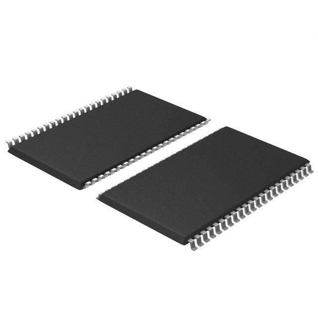
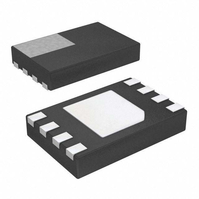
| 供应商器件封装 | 8-SOIC |
| 其它名称 | AT24CS02-SSHM-TDKR |
| 包装 | Digi-Reel® |
| 商标 | Atmel |
| 存储器类型 | EEPROM |
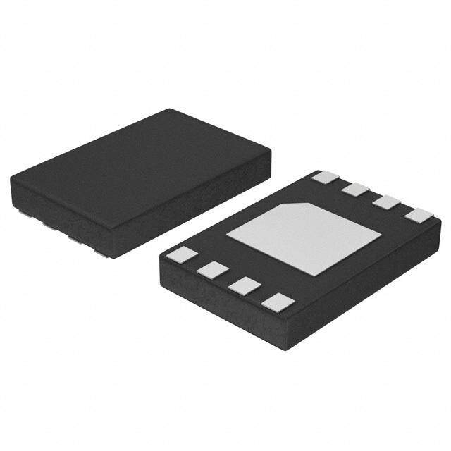
| 存储容量 | 2K (256 x 8) |
| 安装风格 | SMD/SMT |
| 封装 | Reel |
| 封装/外壳 | 8-SOIC(0.154",3.90mm 宽) |
| 封装/箱体 | SOIC-8 |
| 工作温度 | -40°C ~ 85°C |
| 工作电源电压 | 1.7 V to 5.5 V |
| 工厂包装数量 | 4000 |
| 应用说明 | |
| 接口 | I²C,2 线串口 |
| 接口类型 | Serial, 2-Wire, I2C |
| 数据保留 | 100 yr |
| 最大工作温度 | + 85 C |
| 最大工作电流 | 6 uA |
| 最大时钟频率 | 1000 kHz |
| 标准包装 | 1 |
| 格式-存储器 | EEPROMs - 串行 |
| 特色产品 | http://www.digikey.cn/product-highlights/cn/zh/atmel-at24mac-at24cs-eeprom-devices/2284 |
| 电压-电源 | 1.7 V ~ 5.5 V |
| 组织 | 256 x 8 |
| 速度 | 400kHz,1MHz |


- 商务部:美国ITC正式对集成电路等产品启动337调查
- 曝三星4nm工艺存在良率问题 高通将骁龙8 Gen1或转产台积电
- 太阳诱电将投资9.5亿元在常州建新厂生产MLCC 预计2023年完工
- 英特尔发布欧洲新工厂建设计划 深化IDM 2.0 战略
- 台积电先进制程称霸业界 有大客户加持明年业绩稳了
- 达到5530亿美元!SIA预计今年全球半导体销售额将创下新高
- 英特尔拟将自动驾驶子公司Mobileye上市 估值或超500亿美元
- 三星加码芯片和SET,合并消费电子和移动部门,撤换高东真等 CEO
- 三星电子宣布重大人事变动 还合并消费电子和移动部门
- 海关总署:前11个月进口集成电路产品价值2.52万亿元 增长14.8%


PDF Datasheet 数据手册内容提取
AT24CS01 and AT24CS02 I2C-Compatible (2-wire) Serial EEPROM with a Unique, Factory Programmed 128-bit Serial Number 1-Kbit (128 x 8), 2-Kbit (256 x 8) DATASHEET Standard Features Low-voltage Operation ̶ V = 1.7V to 5.5V CC Internally Organized as 128 x 8 (1-Kbit) or 256 x 8 (2-Kbit) I2C-compatible (2-wire) Serial Interface Schmitt Trigger, Filtered Inputs for Noise Suppression Bidirectional Data Transfer Protocol 400kHz (1.7V) and 1MHz (2.5V, 5.0V) Compatibility Write Protect Pin for Hardware Data Protection 8-byte Page Write Mode ̶ Partial Page Writes Allowed Self-timed Write Cycle (5ms Max) High-reliability ̶ Endurance: 1,000,000 Write Cycles ̶ Data Retention: 100 Years Green Package Options (Pb/Halide-free/RoHS-compliant) ̶ 8-lead JEDEC SOIC, 8-lead TSSOP, 8-pad UDFN, and 5-lead SOT23 Die Sale Options: Wafer Form and Tape and Reel Available Enhanced Features in the CS Serial EEPROM Series All Standard Features Supported 128-bit Unique Factory-programmed Serial Number ̶ Permanently Locked, Read-only Value ̶ Stored in a Separate Memory Area ̶ Guaranteed Unique Across Entire CS Series of Serial EEPROMs Atmel-8815E-SEEPROM-AT24CS01-02-Datasheet_012015
1. Description The Atmel® AT24CS01 and AT24CS02 provides 1024/2048 bits of Serial Electrically Erasable and Programmable Read-only Memory (EEPROM) organized as 128/256 words of 8 bits each. The device is optimized for use in many industrial and commercial applications where low-power and low-voltage operation are essential. The AT24CS01/02 is available in space-saving, 8-lead JEDEC SOIC, 8-lead TSSOP, 8-pad UDFN and 5-lead SOT23 packages and is accessed via a 2-wire serial interface. In addition, both devices fully operate from 1.7V to 5.5V V . CC The AT24CS01/02 provides the additional feature of a factory programmed, guaranteed unique 128-bit serial number, while maintaining all of the traditional features available in the 1-Kbit or 2-Kbit Serial EEPROM. The time consuming step of performing and ensuring true serialization of product on a manufacturing line can be removed from the production flow by employing the CS Series Serial EEPROM. The 128-bit serial number is programmed and permanently locked from future writing during the Atmel production process. Further, this 128-bit location does not consume any of the user read/write area of the 1-Kbit or 2-Kbit Serial EEPROM. The uniqueness of the serial number is guaranteed across the entire CS Series of Serial EEPROMs, regardless of the size of the memory array or the type of interface protocol. This means that as an application's needs for memory size or interface protocol evolve in future generations, any previously deployed serial number from any Atmel CS Series Serial EEPROM part will remain valid. 2. Pin Descriptions and Pinouts Figure 2-1. Pin Configuration 8-lead SOIC 8-lead TSSOP Pin Name Function (Top View) (Top View) A - A Address Inputs 0 2 A0 1 8 VCC A0 1 8 VCC SDA Serial Data A1 2 7 WP A1 2 7 WP A2 3 6 SCL GNAD2 34 65 SSCDLA SCL Serial Clock Input GND 4 5 SDA WP Write Protect 8-pad UDFN 5-lead SOT23 GND Ground (Top View) (Top View) VCC Power Supply AA01 12 87 VWCPC SCL 1 5 WP A2 3 6 SCL GND 2 GND 4 5 SDA SDA 3 4 VCC Notes: 1. For use of 5-lead SOT23, the software A2, A1, and A0 bits in the device address word must be set to zero to properly communicate with the device. 2. Drawings are not to scale. 2 AT24CS01/02 [DATASHEET] Atmel-8815E-SEEPROM-AT24CS01-02-Datasheet_012015
3. Absolute Maximum Ratings Operating Temperature.........................-55C to +125C *Notice: Stresses beyond those listed under “Absolute Maximum Ratings” may cause permanent Storage Temperature............................-65C to +150C damage to the device. This is a stress rating only and functional operation of the device at these or Voltage on any pin any other conditions beyond those indicated in the with respect to ground..............................-1.0V to +7.0V operational sections of this specification is not Maximum Operating Voltage.................................6.25V implied. Exposure to absolute maximum rating conditions for extended periods may affect device DC Output Current...............................................5.0mA reliability. 4. Block Diagram Figure 4-1. Block Diagram VCC GND WP Start SCL Stop SDA Logic Serial High Voltage Enable Control Pump & Timing Logic Data Latches Device Load COMP Address INC Comparator Data Word er d Read/Write ADDR/Counter o A2 ec EEPROM D Array A1 w 128-bit o A0 Serial R Read Number Column Serial MUX Decoder D / ACK OUT Logic D D IN OUT AT24CS01/02 [DATASHEET] 3 Atmel-8815E-SEEPROM-AT24CS01-02-Datasheet_012015
5. Pin Descriptions Serial Clock (SCL): The SCL input is used to positive edge clock data into each EEPROM device and negative edge clock data out of each device. Serial Data (SDA): The SDA pin is bidirectional for serial data transfer. This pin is open-drain driven and may be wire-ORed with any number of other open-drain or open-collector devices. Device/Page Addresses (A , A , A ): The A , A and A pins are device address inputs that are hard wired for 2 1 0 2 1 0 the AT24CS01/02. As many as eight 1-Kbit or 2-Kbit devices may be addressed on a single bus system. For more detail, see Section 8., “Device Addressing” on page 10. Write Protect (WP): AT24CS01/02 has a Write Protect (WP) pin that provides hardware data protection. When the Write Protect pin is connected to ground (GND), normal read/write operations to the full array are possible. When the Write Protect pin is connected to V , all write operations to the memory are inhibited but read CC operations are still possible. This operation is summarized in Table 5-1 below. Table 5-1. Write Protect WP Pin Status Part of the Array Protected At V Full Array CC At GND Normal Read/Write Operations 4 AT24CS01/02 [DATASHEET] Atmel-8815E-SEEPROM-AT24CS01-02-Datasheet_012015
6. Memory Organization AT24CS01, 1K Serial EEPROM: Internally organized with 16 pages of 8 bytes each, the 1K requires a 7-bit data word address for random word addressing. AT24CS02, 2K Serial EEPROM: Internally organized with 32 pages of 8 bytes each, the 2K requires an 8-bit data word address for random word addressing. 6.1 Pin Capacitance Table 6-1. Pin Capacitance(1) Applicable over recommended operating range from T = 25°C, f = 1.0MHz, V = 1.7V to 5.5V. A CC Symbol Test Condition Max Units Conditions C Input/Output Capacitance (SDA) 8 pF V = 0V I/O I/O C Input Capacitance (A , A , A , SCL) 6 pF V = 0V IN 0 1 2 IN Note: 1. This parameter is characterized and is not 100% tested. 6.2 DC Characteristics Table 6-2. DC Characteristics Applicable over recommended operating range from: T = -40C to +85C, V = 1.7V to 5.5V (unless otherwise noted). AI CC Symbol Parameter Test Condition Min Typ Max Units V Supply Voltage 1.7 5.5 V CC I Supply Current V = 5.0V Read at 400kHz 0.4 1.0 mA CC1 CC I Supply Current V = 5.0V Write at 400kHz 2.0 3.0 mA CC2 CC I Standby Current V = 1.7V V = V or V 1.0 μA SB1 CC IN CC SS I Standby Current V = 5.5V V = V or V 6.0 μA SB2 CC IN CC SS I Input Leakage Current V = V or V 0.10 3.0 μA LI IN CC SS I Output Leakage Current V = V or V 0.05 3.0 μA LO OUT CC SS V Input Low Level(1) –0.6 V x 0.3 V IL CC V Input High Level(1) V x 0.7 V + 0.5 V IH CC CC V Output Low Level V = 1.7V I = 0.15mA 0.2 V OL1 CC OL V Output Low Level V = 3.0V I = 2.1mA 0.4 V OL2 CC OL Note: 1. V min and V max are reference only and are not tested. IL IH AT24CS01/02 [DATASHEET] 5 Atmel-8815E-SEEPROM-AT24CS01-02-Datasheet_012015
6.3 AC Characteristics Table 6-3. AC Characteristics Applicable over recommended operating range from T = -40C to +85C, V = 1.7V to 5.5V, CL = 1TTL Gate and 100pF AI CC (unless otherwise noted). 1.7V 2.5V, 5.0V Symbol Parameter Min Max Min Max Units f Clock Frequency, SCL 400 1000 kHz SCL t Clock Pulse Width Low 1.2 0.4 μs LOW t Clock Pulse Width High 0.6 0.4 μs HIGH t Noise Suppression Time 100 50 ns I t Clock Low to Data Out Valid 0.1 0.9 0.05 0.55 μs AA Time the bus must be free before a new t 1.3 0.5 μs BUF transmission can start t Start Hold Time 0.6 0.25 μs HD.STA t Start Setup Time 0.6 0.25 μs SU.STA t Data In Hold Time 0 0 μs HD.DAT t Data In Setup Time 100 100 ns SU.DAT t Inputs Rise Time(1) 0.3 0.3 μs R t Inputs Fall Time(1) 300 100 ns F t Stop Setup Time 0.6 0.25 μs SU.STO t Data Out Hold Time 50 50 ns DH t Write Cycle Time 5 5 ms WR Endurance(1) 3.3V, +25C, Page Mode 1,000,000 Write Cycles Note: 1. This parameter is ensured by characterization only. 6 AT24CS01/02 [DATASHEET] Atmel-8815E-SEEPROM-AT24CS01-02-Datasheet_012015
7. Device Operation Clock and Data Transitions: The SDA pin is normally pulled high with an external device. Data on the SDA pin may change only during SCL low time periods. Data changes during SCL high periods will indicate a Start or Stop condition as defined below. Figure 7-1. Data Validity SDA SCL Data Stable Data Stable Data Change Start Condition: A high-to-low transition of SDA with SCL high is a Start condition which must precede any other command. Stop Condition: A low-to-high transition of SDA with SCL high is a Stop condition. After a read sequence, the Stop command will place the EEPROM in a standby power mode. Figure 7-2. Start and Stop Definition SDA SCL Start Stop AT24CS01/02 [DATASHEET] 7 Atmel-8815E-SEEPROM-AT24CS01-02-Datasheet_012015
Acknowledge: All addresses and data words are serially transmitted to and from the EEPROM in 8-bit words. The EEPROM sends a zero to acknowledge that it has received each word. This happens during the ninth clock cycle. Figure 7-3. Output Acknowledge SCL 1 8 9 DATA IN DATA OUT Start Acknowledge Standby Mode: The AT24CS01/02 features a low-power standby mode which is enabled upon power-up as well as after the receipt of the Stop condition and the completion of any internal operations. 2-wire Software Reset: After an interruption in protocol, power loss, or system reset, any 2-wire part can be reset by following these steps: 1. Create a Start condition (if possible). 2. Clock nine cycles. 3. Create another Start condition followed by Stop condition as shown in Figure 7-4. The device should be ready for the next communication after above steps have been completed. In the event that the device is still non-responsive or remains active on the SDA bus, a power cycle must be used to reset the device. Figure 7-4. Software reset Dummy Clock Cycles SCL 1 2 3 8 9 Start Start Stop Condition Condition Condition SDA 8 AT24CS01/02 [DATASHEET] Atmel-8815E-SEEPROM-AT24CS01-02-Datasheet_012015
Figure 7-5. Bus Timing SCL: Serial Clock, SDA: Serial Data I/O t t HIGH t F R t t SCL LOW LOW t t t t t SU.STA HD.STA HD.DAT SU.DAT SU.STO SDA IN t t t AA DH BUF SDA OUT Figure 7-6. Write Cycle Timing SCL: Serial Clock, SDA: Serial Data I/O SCL SDA 8th Bit ACK WORD N (1) t WR Stop Start Condition Condition Note: 1. The write cycle time t is the time from a valid Stop condition of a write sequence to the end of the internal WR clear/write cycle. AT24CS01/02 [DATASHEET] 9 Atmel-8815E-SEEPROM-AT24CS01-02-Datasheet_012015
8. Device Addressing Standard EEPROM Access: The 1K and 2K EEPROM device requires an 8-bit device address word following a Start condition to enable the chip for a read or write operation. The device address word consists of a mandatory ‘1010’ (Ah) sequence for the first four most significant bits as shown in Figure 8-1. This is common to all Serial EEPROM devices. The next three bits are the A2, A1, and A0 device address bits for the 1K and 2K EEPROM. These three bits must compare to their corresponding hard-wired input pins A , A , and A in order for the part to acknowledge. 2 1 0 The eighth bit of the device address is the read/write operation select bit. A read operation is initiated if this bit is high and a write operation is initiated if this bit is low. Upon a valid compare of the device address with hard-wired input pins A , A , and A , the EEPROM will output 2 1 0 a zero. If a compare is not successfully made, the chip will return to a standby state. Serial Number Access: The AT24CS01 and AT24CS02 utilizes a separate memory block containing a factory programmed 128-bit serial number. Access to this memory location is obtained by beginning the device address word with a ‘1011’ (Bh) sequence. The behavior of the next three bits (A2, A1, and A0) remain the same as during a standard EEPROM addressing sequence. These three bits must compare to their corresponding hard-wired input pins A , A , and 2 1 A in order for the part to acknowledge. 0 The eighth bit of the device address needs be set to a one to read the Serial Number. A zero in this bit position, other than during a dummy write sequence to set the address pointer, will result in a unknown data read from the part. Writing or altering the 128-bit serial number is not possible. Further specific protocol is needed to read the serial number from of the device. See Section 10., “Read Operations” on page 12 for more details on accessing the special feature. Figure 8-1. Device Address Density Access Area Bit 7 Bit 6 Bit 5 Bit 4 Bit 3 Bit 2 Bit 1 Bit 0 1K EEPROM 1 0 1 0 A A A R/W 2 1 0 Serial Number 1 0 1 1 A A A 1 2 1 0 2K EEPROM 1 0 1 0 A A A R/W 2 1 0 Serial Number 1 0 1 1 A A A 1 2 1 0 MSB LSB 10 AT24CS01/02 [DATASHEET] Atmel-8815E-SEEPROM-AT24CS01-02-Datasheet_012015
9. Write Operations Byte Write: A Byte Write operation requires an 8-bit data word address following the device address word and acknowledgment. Upon receipt of this address, the EEPROM will again respond with a zero and then clock in the first 8-bit data word. Following receipt of the 8-bit data word, the EEPROM will output a zero and the addressing device, such as a microcontroller, must terminate the write sequence with a Stop condition. At this time the EEPROM enters an internally timed write cycle, t , to the nonvolatile memory. All inputs are disabled WR during this write cycle and the EEPROM will not respond until the Write is complete. Figure 9-1. Byte Write S W T R S A I T R T O T Device Address E Word Address Data P SDA LINE M R A A A S / C C C B WK K K Page Write: The 1K and 2K EEPROM are capable of an 8-byte Page Write. A Page Write is initiated in the same way as a Byte Write, but the microcontroller does not send a Stop condition after the first data word is clocked in. Instead, after the EEPROM acknowledges receipt of the first data word, the microcontroller can transmit up to seven data words. The EEPROM will respond with a zero after each data word received. The microcontroller must terminate the Page Write sequence with a Stop condition. Figure 9-2. Page Write S W T R S A I T R T O T Device Address E Word Address (n) Data (n) Data (n + 1) Data (n + x) P SDA LINE M R A A A A A S / C C C C C B WK K K K K The data word address lower three bits are internally incremented following the receipt of each data word. The higher data word address bits are not incremented, retaining the memory page row location. When the internally generated word address reaches the page boundary, the subsequent byte loaded will be placed at the beginning of the same page. If more than eight data words are transmitted to the EEPROM, the data word address will roll-over and previously loaded data will be overwritten. Acknowledge Polling: Once the internally timed write cycle has started and the EEPROM inputs are disabled, acknowledge polling can be initiated. This involves sending a Start condition followed by the device address word. The Read/Write bit is representative of the operation desired. Only if the internal write cycle has completed will the EEPROM respond with a zero allowing the next read or write sequence to begin. AT24CS01/02 [DATASHEET] 11 Atmel-8815E-SEEPROM-AT24CS01-02-Datasheet_012015
10. Read Operations Read operations are initiated in the same way as Write operations with the exception that the Read/Write select bit in the device address word is set to one. There are four read operations: Current Address Read Random Address Read Sequential Read Serial Number Read Current Address Read: The internal data word address counter maintains the last address accessed during the last Read or Write operation, incremented by one. This address stays valid between operations as long as the chip power is maintained. The address roll-over during read is from the last byte of the last memory page to the first byte of the first page. The address roll-over during write is from the last byte of the current page to the first byte of the same page. Once the device address with the read/write select bit set to one is clocked in and acknowledged by the EEPROM, the current address data word is serially clocked out. The microcontroller does not respond with an zero but does generate a following Stop condition. Figure 10-1. Current Address Read S T R S A E T R A O T Device Address D Data P SDA LINE M R A N S / C O B WK A C K Random Read: A Random Read requires a dummy byte write sequence to load in the data word address. Once the device address word and data word address are clocked in and acknowledged by the EEPROM, the microcontroller must generate another Start condition. The microcontroller now initiates a Current Address Read by sending a device address with the read/write select bit high. The EEPROM acknowledges the device address and serially clocks out the data word. The microcontroller does not respond with a zero but does generate a following Stop condition. Figure 10-2. Random Read S W S T R T R S A I A E T R T R A O T Device Address E Word Address (n) T Device Address D Data (n) P SDA LINE M R A A A N S / C C C O B WK K K A C Dummy Write K 12 AT24CS01/02 [DATASHEET] Atmel-8815E-SEEPROM-AT24CS01-02-Datasheet_012015
Sequential Read: Sequential Reads are initiated by either a current address read or a random address read. After the microcontroller receives a data word, it responds with an acknowledge. As long as the EEPROM receives an acknowledge, it will continue to increment the data word address and serially clock out sequential data words. When the memory address limit is reached, the data word address will roll-over and the Sequential Read will continue. The Sequential Read operation is terminated when the microcontroller does not respond with a zero but does generate a following Stop condition. Figure 10-3. Sequential Read R S E T Device A O Address D Data (n) Data (n + 1) Data (n + 2) Data (n + x) P SDA LINE R A A A A N / C C C C O WK K K K A C K Serial Number Read: Reading the serial number is similar to the sequential read sequence but requires use of the device address seen in Figure 8-1 on page 10, a dummy write, and the use of specific word address. Note: The entire 128-bit value must be read from the starting address of the serial number block to guarantee a unique number. Since the address pointer of the device is shared between the regular EEPROM array and the serial number block, a dummy write sequence, as part of a Random Read or Sequential Read protocol, should be performed to ensure the address pointer is set to zero. A Current Address Read of the serial number block is supported but if the previous operation was to the EEPROM array, the address pointer will retain the last location accessed, incremented by one. Reading the serial number from a location other than the first address of the block will not result in a unique serial number. Additionally, the word address must begin with a ‘10’ sequence regardless of the intended address. If a word address other than ‘10’ is used, then the device will output undefined data. Example: If the application desires to read the first byte of the serial number, the word address input would need to be 80h. When the end of the 128-bit serial number is reached (16 bytes of data), the data word address will roll-over back to the beginning of the 128-bit serial number. The Serial Number Read operation is terminated when the microcontroller does not respond with an zero (ACK) and instead issues a Stop condition (see Figure 10-4 on page 14.) AT24CS01/02 [DATASHEET] 13 Atmel-8815E-SEEPROM-AT24CS01-02-Datasheet_012015
Figure 10-4. Serial Number Read S W S T R T R A I A E R Device T Word R Device A T Address E Address n T Address D SDA LINE 1 0 1 1 1 0 0 0 0 0 0 0 1 0 1 1 M R A A A Serial Number A S / C C C Data Byte 0x0 C B W K K K K Dummy Write S T O P Serial Number Serial Number Serial Number Serial Number N Data Byte 0x1 Data Byte 0x2 Data Byte 0x3 Data Byte 0xF O A C K 14 AT24CS01/02 [DATASHEET] Atmel-8815E-SEEPROM-AT24CS01-02-Datasheet_012015
11. Part Markings AT24CS01 and AT24CS02: Package Marking Information 8-lead SOIC 8-lead TSSOP ATHYWW ATMLHYWW ## M @ ## M @ AAAAAAAA AAAAAAA 8-lead UDFN 5-lead SOT-23 2.0 x 3.0 mm Body ## ## MU Top Mark HM@ YXX YMXX Bottom Mark Note 1: designates pin 1 Note 2: Package drawings are not to scale Catalog Number Truncation AT24CS01 Truncation Code ##: N1 AT24CS02 Truncation Code ##: N2 Date Codes Voltages Y = Year M = Month WW = Work Week of Assembly M: 1.7V min 2: 2012 6: 2016 A: January 02: Week 2 3: 2013 7: 2017 B: February 04: Week 4 4: 2014 8: 2018 ... ... 5: 2015 9: 2019 L: December 52: Week 52 Country of Assembly Lot Number Grade/Lead Finish Material @ = Country of Assembly AAA...A = Atmel Wafer Lot Number H: Industrial/NiPdAu U: Industrial/Matte Tin Trace Code Atmel Truncation XX = Trace Code (Atmel Lot Numbers Correspond to Code) AT: Atmel Example: AA, AB.... YZ, ZZ ATM: Atmel ATML: Atmel 4/3/12 TITLE DRAWING NO. REV. 24CS01-02SM, AT24CS01, and AT24CS02 Package Mark Contact: 24CS01-02SM A Package Marking Information DL-CSO-Assy_eng@atmel.com AT24CS01/02 [DATASHEET] 15 Atmel-8815E-SEEPROM-AT24CS01-02-Datasheet_012015
12. Ordering Code Detail A T 2 4 C S 0 1 - S S H M - B Atmel Designator Shipping Carrier Option B = Bulk (Tubes) T = Tape and Reel, Standard Quantity Option E = Tape and Reel, Expanded Quantity Option Product Family 24CS = Serial EEPROM, Plus 128-bit Serial Number Feature Operating Voltage M = 1.7V to 5.5V Device Density Package Device Grade or 01 = 1K Wafer/Die Thickness 02 = 2K H = Green, NiPdAu Lead Finish, Industrial Temperature Range (-40˚C to +85°C) U = Green, Matte Sn Lead Finish, Industrial Temperature Range (-40˚C to +85°C) 11 = 11mil Wafer Thickness Package Option SS = JEDEC SOIC X = TSSOP MA = UDFN ST = SOT23 WWU = Wafer Unsawn 16 AT24CS01/02 [DATASHEET] Atmel-8815E-SEEPROM-AT24CS01-02-Datasheet_012015
13. Ordering Information Additional package types that are not listed may be available. Please contact Atmel for more details. Delivery Information Operation Atmel Ordering Code Finish Package Form Quantity Range AT24CS01-SSHM-B Bulk (Tubes) 100 per Tube 8S1 AT24CS01-SSHM-T Tape and Reel 4,000 per Reel AT24CS01-XHM-B Bulk (Tubes) 100 per Tube 8X NiPdAu AT24CS01-XHM-T Tape and Reel 5,000 per Reel Industrial (Lead-free/Halogen-free) Temperature AT24CS01-MAHM-T Tape and Reel 5,000 per Reel (-40C to +85C) 8MA2 AT24CS01-MAHM-E Tape and Reel 15,000 per Reel AT24CS01-STUM-T 5TS1 Tape and Reel 5,000 per Reel AT24CS01-WWU11M(1) N/A Wafer Sale Note 1 AT24CS02-SSHM-B Bulk (Tubes) 100 per Tube 8S1 AT24CS02-SSHM-T Tape and Reel 4,000 per Reel AT24CS02-XHM-B Bulk (Tubes) 100 per Tube 8X NiPdAu AT24CS02-XHM-T Tape and Reel 5,000 per Reel Industrial (Lead-free/Halogen-free) Temperature AT24CS02-MAHM-T Tape and Reel 5,000 per Reel (-40C to +85C) 8MA2 AT24CS02-MAHM-E Tape and Reel 15,000 per Reel AT24CS02-STUM-T 5TS1 Tape and Reel 5,000 per Reel AT24CS02-WWU11M(1) N/A Wafer Sale Note 1 Note: 1. For Wafer sales, please contact Atmel Sales. Package Type 8S1 8-lead, 0.150” wide, Plastic Gull Wing Small Outline (JEDEC SOIC) 8X 8-lead, 4.4mm body, Plastic Thin Shrink Small Outline Package (TSSOP) 8MA2 8-pad, 2.00mm x 3.00mm body, 0.50mm pitch, Dual No Lead (UDFN) 5TS1 5-lead, 2.90mm x 1.60mm body, Plastic Thin Shrink Small Outline (SOT23) AT24CS01/02 [DATASHEET] 17 Atmel-8815E-SEEPROM-AT24CS01-02-Datasheet_012015
14. Packaging Information 14.1 8S1 — 8-lead JEDEC SOIC C 1 E E1 L N Ø TOP VIEW END VIEW e b A COMMON DIMENSIONS (Unit of Measure = mm) SYMBOL MIN NOM MAX NOTE A1 A 1.35 – 1.75 A1 0.10 – 0.25 b 0.31 – 0.51 C 0.17 – 0.25 D 4.80 – 5.05 D E1 3.81 – 3.99 E 5.79 – 6.20 SIDE VIEW e 1.27 BSC Notes: This drawing is for general information only. L 0.40 – 1.27 Refer to JEDEC Drawing MS-012, Variation AA ØØ 0° – 8° for proper dimensions, tolerances, datums, etc. 6/22/11 TITLE GPC DRAWING NO. REV. 8S1, 8-lead (0.150” Wide Body), Plastic Gull Wing SWB 8S1 G Package Drawing Contact: Small Outline (JEDEC SOIC) packagedrawings@atmel.com 18 AT24CS01/02 [DATASHEET] Atmel-8815E-SEEPROM-AT24CS01-02-Datasheet_012015
14.2 8X — 8-lead TSSOP C 1 Pin 1 indicator this corner E1 E L1 N L Top View End View A b A1 COMMON DIMENSIONS e A2 (Unit of Measure = mm) D SYMBOL MIN NOM MAX NOTE Side View A - - 1.20 A1 0.05 - 0.15 Notes: 1. This drawing is for general information only. A2 0.80 1.00 1.05 Refer to JEDEC Drawing MO-153, Variation AA, for proper dimensions, tolerances, datums, etc. D 2.90 3.00 3.10 2, 5 2. Dimension D does not include mold Flash, protrusions or gate E 6.40 BSC burrs. Mold Flash, protrusions and gate burrs shall not exceed 0.15mm (0.006in) per side. E1 4.30 4.40 4.50 3, 5 3. Dimension E1 does not include inter-lead Flash or protrusions. Inter-lead Flash and protrusions shall not exceed 0.25mm b 0.19 0.25 0.30 4 (0.010in) per side. e 0.65 BSC 4. Dimension b does not include Dambar protrusion. Allowable Dambar protrusion shall be 0.08mm total in excess L 0.45 0.60 0.75 of the b dimension at maximum material condition. Dambar L1 1.00 REF cannot be located on the lower radius of the foot. Minimum space between protrusion and adjacent lead is 0.07mm. C 0.09 - 0.20 5. Dimension D and E1 to be determined at Datum Plane H. 2/27/14 TITLE GPC DRAWING NO. REV. 8X, 8-lead 4.4mm Body, Plastic Thin Package Drawing Contact: Shrink Small Outline Package (TSSOP) TNR 8X E packagedrawings@atmel.com AT24CS01/02 [DATASHEET] 19 Atmel-8815E-SEEPROM-AT24CS01-02-Datasheet_012015
14.3 8MA2 — 8-pad UDFN E 1 8 Pin 1 ID 2 7 D 3 6 4 5 TOP VIEW C SIDE VIEW A2 A A1 E2 b (8x) 8 1 COMMON DIMENSIONS 7 2 Pin#1 ID (Unit of Measure = mm) D2 6 3 SYMBOL MIN NOM MAX NOTE A 0.50 0.55 0.60 5 4 A1 0.0 0.02 0.05 e (6x) A2 - - 0.55 L (8x) K D 1.90 2.00 2.10 BOTTOM VIEW D2 1.40 1.50 1.60 Notes: 1. This drawing is for general information only. Refer to E 2.90 3.00 3.10 Drawing MO-229, for proper dimensions, tolerances, E2 1.20 1.30 1.40 datums, etc. 2. The Pin #1 ID is a laser-marked feature on Top View. b 0.18 0.25 0.30 3 3. Dimensions b applies to metallized terminal and is C 1.52 REF measured between 0.15 mm and 0.30 mm from the terminal tip. If the terminal has the optional radius on L 0.30 0.35 0.40 the other end of the terminal, the dimension should e 0.50 BSC not be measured in that radius area. 4. The Pin #1 ID on the Bottom View is an orientation K 0.20 - - feature on the thermal pad. 11/26/14 TITLE GPC DRAWING NO. REV. 8MA2, 8-pad 2 x 3 x 0.6mm Body, Thermally Package Drawing Contact: Enhanced Plastic Ultra Thin Dual Flat No-Lead YNZ 8MA2 G packagedrawings@atmel.com Package (UDFN) 20 AT24CS01/02 [DATASHEET] Atmel-8815E-SEEPROM-AT24CS01-02-Datasheet_012015
14.4 5TS1 — 5-lead SOT23 e1 5 4 C E1 E CL L1 1 2 3 TOP VIEW END VIEW b A2 A SEATING PLANE e A1 D SIDE VIEW COMMON DIMENSIONS (Unit of Measure = mm) 1. Dimension D does not include mold flash, protrusions or gate burrs. Mold flash, protrusions or gate burrs shall not exceed 0.15 mm per end. Dimension E1 does SYMBOL MIN NOM MAX NOTE not include interlead flash or protrusion. Interlead flash or protrusion shall not A - - 1.00 exceed 0.15 mm per side. 2. The package top may be smaller than the package bottom. Dimensions D and E1 A1 0.00 - 0.10 are determined at the outermost extremes of the plastic body exclusive of mold A2 0.70 0.90 1.00 flash, tie bar burrs, gate burrs and interlead flash, but including any mismatch between the top and bottom of the plastic body. c 0.08 - 0.20 3 3. These dimensions apply to the flat section of the lead between 0.08 mm and 0.15 D 2.90 BSC 1,2 mm from the lead tip. 4. Dimension "b" does not include dambar protrusion. Allowable dambar protrusion E 2.80 BSC 1,2 shall be 0.08 mm total in excess of the "b" dimension at maximum material condition. The dambar cannot be located on the lower radius of the foot. Minimum E1 1.60 BSC 1,2 space between protrusion and an adjacent lead shall not be less than 0.07 mm. L1 0.60 REF e 0.95 BSC e1 1.90 BSC This drawing is for general information only. Refer to JEDEC b 0.30 - 0.50 3,4 Drawing MO-193, Variation AB for additional information. 5/31/12 TITLE GPC DRAWING NO. REV. 5TS1, 5-lead 1.60mm Body, Plastic Thin Package Drawing Contact: Shrink Small Outline Package (Shrink SOT) TSZ 5TS1 D packagedrawings@atmel.com AT24CS01/02 [DATASHEET] 21 Atmel-8815E-SEEPROM-AT24CS01-02-Datasheet_012015
15. Revision History Doc. Rev. Date Comments Add the UDFN Expanded Quantity Option and update the ordering information section. 8815E 01/2015 Update the 8MA2 package outline drawing. Add bulk SOIC and TSSOP ordering codes. Update ordering code table, 8X and 8MA2 package drawings, and update the disclaimer page. 8815D 08/2014 Correct pinouts from bottom to top view and reorganization figures. No changes to functional specification. 8815C 07/2013 Update status from preliminary to complete release and footers and the disclaimer page. 8815B 09/2012 Update ordering information. 8815A 06/2012 Initial document release. 22 AT24CS01/02 [DATASHEET] Atmel-8815E-SEEPROM-AT24CS01-02-Datasheet_012015
X X X X X X Atmel Corporation 1600 Technology Drive, San Jose, CA 95110 USA T: (+1)(408) 441.0311 F: (+1)(408) 436.4200 | www.atmel.com © 2015 Atmel Corporation. / Rev.: Atmel-8815E-SEEPROM-AT24CS01-02-Datasheet_012015. Atmel®, Atmel logo and combinations thereof, Enabling Unlimited Possibilities®, and others are registered trademarks or trademarks of Atmel Corporation in U.S. and other countries. Other terms and product names may be trademarks of others. DISCLAIMER: The information in this document is provided in connection with Atmel products. No license, express or implied, by estoppel or otherwise, to any intellectual property right is granted by this document or in connection with the sale of Atmel products. EXCEPT AS SET FORTH IN THE ATMEL TERMS AND CONDITIONS OF SALES LOCATED ON THE ATMEL WEBSITE, ATMEL ASSUMES NO LIABILITY WHATSOEVER AND DISCLAIMS ANY EXPRESS, IMPLIED OR STATUTORY WARRANTY RELATING TO ITS PRODUCTS INCLUDING, BUT NOT LIMITED TO, THE IMPLIED WARRANTY OF MERCHANTABILITY, FITNESS FOR A PARTICULAR PURPOSE, OR NON-INFRINGEMENT. IN NO EVENT SHALL ATMEL BE LIABLE FOR ANY DIRECT, INDIRECT, CONSEQUENTIAL, PUNITIVE, SPECIAL OR IAT24CS01/02NCIDENTAL DAMAGES (INCLUDING, WITHOUT LIMITATION, DAMAGES FOR LOSS AND PROFITS, BUSINESS INTERRUPTION, OR LOSS OF INFORMATION) ARISING OUT OF THE USE OR INABILITY TO USE THIS DOCUMENT, EVEN IF ATMEL HAS BEEN ADVISED OF THE POSSIBILITY OF SUCH DAMAGES. Atmel makes no representations or warranties with respect to the accuracy or completeness of the contents of this document and reserves the right to make changes to specifications and products descriptions at any time without notice. Atmel does not make any commitment to update the information contained herein. Unless specifically provided otherwise, Atmel products are not suitable for, and shall not be used in, automotive applications. Atmel products are not intended, authorized, or warranted for use as components in applications intended to support or sustain life. SAFETY-CRITICAL, MILITARY, AND AUTOMOTIVE APPLICATIONS DISCLAIMER: Atmel products are not designed for and will not be used in connection with any applications where the failure of such products would reasonably be expected to result in significant personal injury or death (“Safety-Critical Applications”) without an Atmel officer's specific written consent. Safety-Critical Applications include, without limitation, life support devices and systems, equipment or systems for the operation of nuclear facilities and weapons systems. Atmel products are not designed nor intended for use in military or aerospace applications or environments unless specifically designated by Atmel as military-grade. Atmel products are not designed nor intended for use in automotive applications unless specifically designated by Atmel as automotive-grade.
Mouser Electronics Authorized Distributor Click to View Pricing, Inventory, Delivery & Lifecycle Information: M icrochip: AT24CS01-SSHM-T AT24CS01-XHM-T AT24CS02-SSHM-T AT24CS02-XHM-T AT24CS01-MAHM-T AT24CS02- MAHM-T AT24CS01-STUM-T AT24CS02-STUM-T AT24CS01-XHM-B AT24CS02-XHM-B AT24CS02-SSHM-B AT24CS01-SSHM-B AT24CS02-MAHM-E AT24CS01-MAHM-E