
 Datasheet下载
- 型号: AT24C08D-MAHM-T
- 制造商: Atmel
- 库位|库存: xxxx|xxxx
- 要求:
| 数量阶梯 | 香港交货 | 国内含税 |
| +xxxx | $xxxx | ¥xxxx |
查看当月历史价格
查看今年历史价格
AT24C08D-MAHM-T产品简介:
ICGOO电子元器件商城为您提供AT24C08D-MAHM-T由Atmel设计生产,在icgoo商城现货销售,并且可以通过原厂、代理商等渠道进行代购。 AT24C08D-MAHM-T价格参考。AtmelAT24C08D-MAHM-T封装/规格:存储器, EEPROM 存储器 IC 8Kb (1K x 8) I²C 1MHz 4.5µs 8-UDFN(2x3)。您可以下载AT24C08D-MAHM-T参考资料、Datasheet数据手册功能说明书,资料中有AT24C08D-MAHM-T 详细功能的应用电路图电压和使用方法及教程。
| 参数 | 数值 |
| 产品目录 | 集成电路 (IC) |
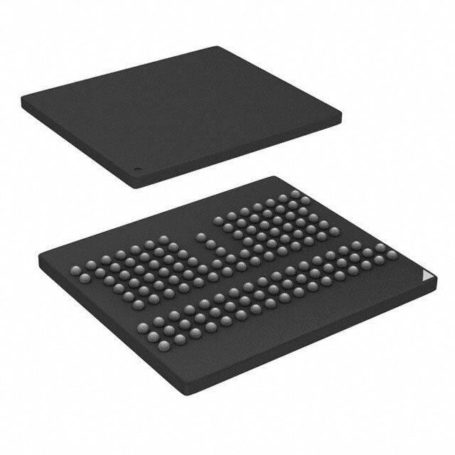
| 描述 | IC EEPROM 8KBIT 1MHZ 8UDFN |
| 产品分类 | |
| 品牌 | Atmel |
| 数据手册 | |
| 产品图片 | |
| 产品型号 | AT24C08D-MAHM-T |
| rohs | 无铅 / 符合限制有害物质指令(RoHS)规范要求 |
| 产品系列 | - |
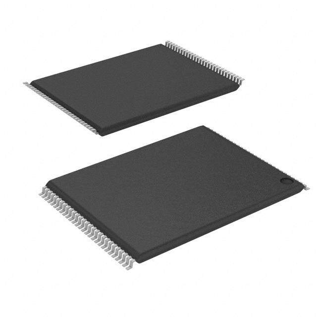
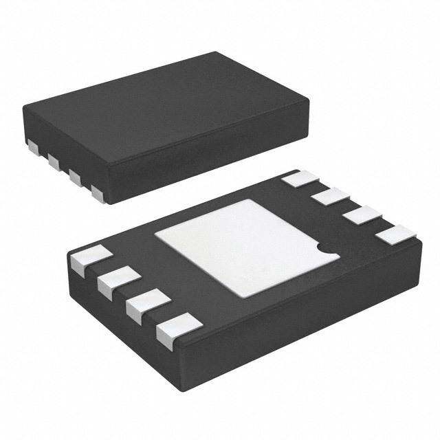
| 供应商器件封装 | 8-UDFN(2x3) |
| 其它名称 | AT24C08D-MAHM-TCT |
| 包装 | 剪切带 (CT) |
| 存储器类型 | EEPROM |
| 存储容量 | 8K (1K x 8) |
| 封装/外壳 | 8-UFDFN 裸露焊盘 |
| 工作温度 | -40°C ~ 85°C |
| 接口 | I²C,2 线串口 |
| 标准包装 | 1 |
| 格式-存储器 | EEPROMs - 串行 |
| 电压-电源 | 1.7 V ~ 3.6 V |
| 速度 | 400kHz,1MHz |

_renders/IS42S16800F-7BLI.jpg)


- 商务部:美国ITC正式对集成电路等产品启动337调查
- 曝三星4nm工艺存在良率问题 高通将骁龙8 Gen1或转产台积电
- 太阳诱电将投资9.5亿元在常州建新厂生产MLCC 预计2023年完工
- 英特尔发布欧洲新工厂建设计划 深化IDM 2.0 战略
- 台积电先进制程称霸业界 有大客户加持明年业绩稳了
- 达到5530亿美元!SIA预计今年全球半导体销售额将创下新高
- 英特尔拟将自动驾驶子公司Mobileye上市 估值或超500亿美元
- 三星加码芯片和SET,合并消费电子和移动部门,撤换高东真等 CEO
- 三星电子宣布重大人事变动 还合并消费电子和移动部门
- 海关总署:前11个月进口集成电路产品价值2.52万亿元 增长14.8%


PDF Datasheet 数据手册内容提取
AT24C08D I²C-Compatible (2-Wire) Serial EEPROM 8-Kbit (1,024 x 8) Features • Low-Voltage Operation: – Vcc = 1.7V to 3.6V • Internally Organized as 1,024 x 8 (8K) • Industrial Temperature Range -40°C to +85°C • I2C-Compatible (2-Wire) Serial Interface: – 100 kHz Standard mode, 1.7V to 3.6V – 400 kHz Fast mode, 1.7V to 3.6V – 1 MHz Fast Mode Plus (FM+), 2.5V to 3.6V • Schmitt Triggers, Filtered Inputs for Noise Suppression • Bidirectional Data Transfer Protocol • Write-Protect Pin for Full Array Hardware Data Protection (except WLCSP) • Ultra Low Active Current (1 mA maximum) and Standby Current (0.8 μA maximum) • 16-Byte Page Write Mode: – Partial page writes allowed • Random and Sequential Read Modes • Self-Timed Write Cycle within 5 ms Maximum • ESD Protection > 4,000V • High Reliability: – Endurance: 1,000,000 write cycles – Data retention: 100 years • Green Package Options (Lead-free/Halide-free/RoHS compliant) • Die Sale Options: Wafer Form and Bumped Wafers Packages • 8-Lead PDIP(1), 8-Lead SOIC, 5-Lead SOT23, 8-Lead TSSOP, 8-Pad UDFN, 8-Ball VFBGA and 4- Ball WLCSP Note: 1. Contact Microchip Sales for the availability of this package. © 2018 Microchip Technology Inc. Datasheet DS20006022A-page 1
AT24C08D Table of Contents Features..........................................................................................................................1 Packages.........................................................................................................................1 1. Package Types (not to scale)....................................................................................4 2. Pin Descriptions.........................................................................................................5 2.1. Device Address Input (A2)...........................................................................................................5 2.2. Ground.........................................................................................................................................5 2.3. Serial Data (SDA).........................................................................................................................5 2.4. Serial Clock (SCL)........................................................................................................................6 2.5. Write-Protect (WP).......................................................................................................................6 2.6. Device Power Supply...................................................................................................................6 3. Description.................................................................................................................7 3.1. System Configuration Using 2-Wire Serial EEPROMs.................................................................7 3.2. Block Diagram..............................................................................................................................8 4. Electrical Characteristics...........................................................................................9 4.1. Absolute Maximum Ratings..........................................................................................................9 4.2. DC and AC Operating Range.......................................................................................................9 4.3. DC Characteristics.......................................................................................................................9 4.4. AC Characteristics......................................................................................................................10 4.5. Electrical Specifications..............................................................................................................12 5. Device Operation and Communication....................................................................14 5.1. Clock and Data Transition Requirements...................................................................................14 5.2. Start and Stop Conditions..........................................................................................................14 5.3. Acknowledge and No-Acknowledge...........................................................................................15 5.4. Standby Mode............................................................................................................................15 5.5. Software Reset...........................................................................................................................16 6. Memory Organization..............................................................................................17 6.1. Device Addressing.....................................................................................................................17 7. Write Operations......................................................................................................19 7.1. Byte Write...................................................................................................................................19 7.2. Page Write..................................................................................................................................19 7.3. Acknowledge Polling..................................................................................................................20 7.4. Write Cycle Timing.....................................................................................................................20 7.5. Write Protection..........................................................................................................................21 8. Read Operations.....................................................................................................23 8.1. Current Address Read................................................................................................................23 8.2. Random Read............................................................................................................................23 © 2018 Microchip Technology Inc. Datasheet DS20006022A-page 2
AT24C08D 8.3. Sequential Read.........................................................................................................................24 9. Device Default Condition from Microchip................................................................25 10.Packaging Information.............................................................................................26 10.1. Package Marking Information.....................................................................................................26 11. Revision History.......................................................................................................40 The Microchip Web Site................................................................................................41 Customer Change Notification Service..........................................................................41 Customer Support.........................................................................................................41 Product Identification System........................................................................................42 Microchip Devices Code Protection Feature.................................................................42 Legal Notice...................................................................................................................43 Trademarks...................................................................................................................43 Quality Management System Certified by DNV.............................................................44 Worldwide Sales and Service........................................................................................45 © 2018 Microchip Technology Inc. Datasheet DS20006022A-page 3
AT24C08D Package Types (not to scale) 1. Package Types (not to scale) 8-lead PDIP/SOIC/TSSOP (Top View) 5-lead SOT23(2) NC 1 8 Vcc (Top View) NC 2 7 WP SCL 1 5 WP A2 3 6 SCL GND 2 GND 4 5 SDA SDA 3 4 Vcc 8-pad UDFN (Top View) NC 1 8 Vcc NC 2 7 WP A2 3 6 SCL GND 4 5 SDA 8-ball VFBGA 4-ball WLCSP(1) (Top View) (Top View) NC 1 8 Vcc Vcc A1 A2 GND NC 2 7 WP 3 6 A2 SCL SCL B1 B2 SDA GND 4 5 SDA Note: 1. Since the WLCSP has no WP pin, the write protection feature is not offered on the WLCSP. Refer to 6.1 Device Addressing for details about addressing the WLCSP version of the device. 2. Refer to 6.1 Device Addressing for details about addressing the SOT23 version of the device. © 2018 Microchip Technology Inc. Datasheet DS20006022A-page 4
AT24C08D Pin Descriptions 2. Pin Descriptions The descriptions of the pins are listed in Table 2-1. Table 2-1. Pin Function Table Name 8-Lead 8-Lead 8-Lead 5-Lead 8-Pad 8Ball 4-Ball Function PDIP SOIC TSSOP SOT23 UDFN(1) VFBGA WLCSP NC 1 1 1 - 1 1 - No Connect NC 2 2 2 - 2 2 - No Connect A2(2) 3 3 3 - 3 3 - Device Address Input GND 4 4 4 2 4 4 A2 Ground SDA 5 5 5 3 5 5 B2 Serial Data SCL 6 6 6 1 6 6 B1 Serial Clock WP(2) 7 7 7 5 7 7 - Write-Protect V 8 8 8 4 8 8 A1 Device Power CC Supply Note: 1. The exposed pad on the this package can be connected to GND or left floating. 2. If the A2 or WP pins are not driven, they are internally pulled down to GND. In order to operate in a wide variety of application environments, the pull-down mechanism is intentionally designed to be somewhat strong. Once these pins are biased above the CMOS input buffer’s trip point (~0.5 x V ), the pull‑down mechanism disengages. Microchip recommends connecting these CC pins to a known state whenever possible. 2.1 Device Address Input (A2) The A2 pin is a device address input that is hard-wired (directly to GND or to V ) for compatibility with CC other AT24C devices. When the pin is hard-wired, as many as two devices may be addressed on a single bus system. A device is selected when a corresponding hardware and software match is true. If the pin is left floating, the A2 pin will be internally pulled down to GND. However, due to capacitive coupling that may appear in customer applications, Microchip recommends always connecting the address pin to a known state. When using a pull-up resistor, Microchip recommends using 10 kΩ or less. 2.2 Ground The ground reference for the power supply. GND should be connected to the system ground. 2.3 Serial Data (SDA) The SDA pin is an open-drain bidirectional input/output pin used to serially transfer data to and from the device. The SDA pin must be pulled-high using an external pull-up resistor (not to exceed 10 kΩ in value) and may be wire-ORed with any number of other open-drain or open-collector pins from other devices on the same bus. © 2018 Microchip Technology Inc. Datasheet DS20006022A-page 5
AT24C08D Pin Descriptions 2.4 Serial Clock (SCL) The SCL pin is used to provide a clock to the device and to control the flow of data to and from the device. Command and input data present on the SDA pin is always latched in on the rising edge of SCL, while output data on the SDA pin is clocked out on the falling edge of SCL. The SCL pin must either be forced high when the serial bus is idle or pulled high using an external pull-up resistor. 2.5 Write-Protect (WP) The write-protect input, when connected to GND, allows normal write operations. When the WP pin is connected directly to V , all write operations to the protected memory are inhibited. CC If the pin is left floating, the WP pin will be internally pulled down to GND. However, due to capacitive coupling that may appear in customer applications, Microchip recommends always connecting the WP pin to a known state. When using a pull‑up resistor, Microchip recommends using 10 kΩ or less. Table 2-2. Write-Protect WP Pin Status Part of the Array Protected At V Full Array CC At GND Normal Write Operations 2.6 Device Power Supply The V pin is used to supply the source voltage to the device. Operations at invalid V voltages may CC CC produce spurious results and should not be attempted. © 2018 Microchip Technology Inc. Datasheet DS20006022A-page 6
AT24C08D Description 3. Description The AT24C08D provides 8,192 bits of Serial Electrically Erasable and Programmable Read-Only Memory (EEPROM) organized as 1,024 words of 8 bits each. This device is optimized for use in many industrial and commercial applications where low-power and low-voltage operations are essential. The device is available in space-saving 8-lead SOIC, 8-lead TSSOP, 8-pad UDFN, 8-lead PDIP(1), 5-lead SOT23, 8-ball VFBGA and 4-ball WLCSP packages. All packages operate from 1.7V to 3.6V. Note: 1. Contact Microchip Sales for the availability of this package. 3.1 System Configuration Using 2-Wire Serial EEPROMs VCC RPUP(max) = tR(max) 0.8473 x CL VCC RPUP(min) = VCC - VOL(max) IOL SCL SDA WP I2C Bus Master: Microcontroller NC VCC NC VCC NC Slave 0 WP NC Slave 1 WP AT24CXXX AT24CXXX A2 SDA A2 SDA GND SCL GND SCL GND © 2018 Microchip Technology Inc. Datasheet DS20006022A-page 7
AT24C08D Description 3.2 Block Diagram Hardware Address Memory POR V Comparator System Control Generator CC Module High-Voltage Generation Circuit Write Protection WP er d Control o EEPROM Array ec D w o R Address Register and Counter 1 page Column Decoder A2 SCL Data Register Start Stop Data & ACK Detector D Input/Output Control OUT D GND IN SDA © 2018 Microchip Technology Inc. Datasheet DS20006022A-page 8
AT24C08D Electrical Characteristics 4. Electrical Characteristics 4.1 Absolute Maximum Ratings Temperature under bias -55°C to +125°C Storage temperature -65°C to +150°C V 4.1V CC Voltage on any pin with respect to ground -0.6V to +4.1V DC output current 5.0 mA ESD protection >4 kV Note: Stresses above those listed under “Absolute Maximum Ratings” may cause permanent damage to the device. This is a stress rating only and functional operation of the device at these or any other conditions above those indicated in the operation listings of this specification is not implied. Exposure to absolute maximum rating conditions for extended periods may affect device reliability. 4.2 DC and AC Operating Range Table 4-1. DC and AC Operating Range AT24C08D Operating Temperature (Case) Industrial Temperature Range -40°C to +85°C V Power Supply Low Voltage Grade 1.7V to 3.6V CC 4.3 DC Characteristics Table 4-2. DC Characteristics Parameter Symbol Minimum Typical(1) Maximum Units Test Conditions Supply V 1.7 — 3.6 V CC Voltage Supply I — 0.08 0.3 mA V = 1.8V(2), Read at CC1 CC Current 400 kHz — 0.15 0.5 mA V = 3.6V, Read at 1 MHz CC Supply I — 0.20 1.0 mA V = 3.6V, Write at 1 MHz CC2 CC Current Standby I — 0.08 0.4 μA V = 1.8V(2), V = V or SB CC IN CC Current GND — 0.10 0.8 μA V = 3.6V, V = V or CC IN CC GND © 2018 Microchip Technology Inc. Datasheet DS20006022A-page 9
AT24C08D Electrical Characteristics Parameter Symbol Minimum Typical(1) Maximum Units Test Conditions Input I — 0.10 3.0 μA V = V or GND LI IN CC Leakage Current Output I — 0.05 3.0 μA V = V or GND LO OUT CC Leakage Current Input Low V -0.6 — V x 0.3 V Note 2 IL CC Level Input High V V x 0.7 — V + 0.5 V Note 2 IH CC CC Level Output Low V — — 0.2 V V = 1.8V, I = 0.15 mA OL1 CC OL Level Output Low V — — 0.4 V V = 3.0V, I = 2.1 mA OL2 CC OL Level Note: 1. Typical values characterized at T = +25°C unless otherwise noted. A 2. This parameter is characterized but is not 100% tested in production. 4.4 AC Characteristics Table 4-3. AC Characteristics(1) Parameter Symbol Standard Mode Fast Mode Fast Mode Plus Units V = 1.7V to 3.6V V = 1.7V to 3.6V V = 2.5V to 3.6V CC CC CC Min. Max. Min. Max. Min. Max. Clock f — 100 — 400 — 1000 kHz SCL Frequency, SCL Clock Pulse t 4,700 — 1,300 — 500 — ns LOW Width Low Clock Pulse t 4,000 — 600 — 400 — ns HIGH Width High Input Filter t — 100 — 100 — 100 ns I Spike Suppression (SCL,SDA)(2) Clock Low to t — 4,500 — 900 — 450 ns AA Data Out Valid Bus Free Time t 4,700 — 1,300 — 500 — ns BUF between Stop and Start(2) © 2018 Microchip Technology Inc. Datasheet DS20006022A-page 10
AT24C08D Electrical Characteristics Parameter Symbol Standard Mode Fast Mode Fast Mode Plus Units V = 1.7V to 3.6V V = 1.7V to 3.6V V = 2.5V to 3.6V CC CC CC Min. Max. Min. Max. Min. Max. Start Hold t 4,000 — 600 — 250 — ns HD.STA Time Start Set-up t 4,700 — 600 — 250 — ns SU.STA Time Data In Hold t 0 — 0 — 0 — ns HD.DAT Time Data In Set-up t 200 — 100 — 100 — ns SU.DAT Time Inputs Rise t — 1,000 — 300 — 100 ns R Time(2) Inputs Fall t — 300 — 300 — 100 ns F Time(2) Stop Set-up t 4,700 — 600 — 250 — ns SU.STO Time Write-Protect t 4,000 — 600 — 100 — ns SU.WP Setup Time Write-Protect t 4,000 — 600 — 400 — ns HD.WP Hold Time Data Out Hold t 100 — 50 — 50 — ns DH Time Write Cycle t — 5 — 5 — 5 ms WR Time Note: 1. AC measurement conditions: – C : 100 pF L – R (SDA bus line pull-up resistor to V ): 1.3 kΩ (1000 kHz), 4 kΩ (400 kHz), PUP CC 10 kΩ (100 kHz) – Input pulse voltages: 0.3 x V to 0.7 x V CC CC – Input rise and fall times: ≤50 ns – Input and output timing reference voltages: 0.5 x V CC 2. These parameters are determined through product characterization and are not 100% tested in production. © 2018 Microchip Technology Inc. Datasheet DS20006022A-page 11
AT24C08D Electrical Characteristics Figure 4-1. Bus Timing t t HIGH t F R t LOW SCL t t t t t SU.STA HD.STA HD.DAT SU.DAT SU.STO SDA In t t AA BUF t DH SDA Out 4.5 Electrical Specifications 4.5.1 Power-Up Requirements and Reset Behavior During a power-up sequence, the V supplied to the AT24C08D should monotonically rise from GND to CC the minimum V level, as specified in Table 4-1, with a slew rate no faster than 0.1 V/µs. CC 4.5.1.1 Device Reset To prevent inadvertent write operations or any other spurious events from occurring during a power-up sequence, the AT24C08D includes a Power-on Reset (POR) circuit. Upon power-up, the device will not respond to any commands until the V level crosses the internal voltage threshold (V ) that brings the CC POR device out of Reset and into Standby mode. The system designer must ensure the instructions are not sent to the device until the V supply has CC reached a stable value greater than or equal to the minimum V level. Additionally, once the V is CC CC greater than or equal to the minimum V level, the bus master must wait at least t before sending the CC PUP first command to the device. See Table 4-4 for the values associated with these power-up parameters. Table 4-4. Power-up Conditions(1) Symbol Parameter Min. Max. Units t Time required after V is stable before the device can accept commands. 100 - µs PUP CC V Power-on Reset Threshold Voltage. — 1.5 V POR t Minimum time at V = 0V between power cycles. 1 — ms POFF CC Note: 1. These parameters are characterized but they are not 100% tested in production. If an event occurs in the system where the V level supplied to the AT24C08D drops below the CC maximum V level specified, it is recommended that a full power cycle sequence be performed by first POR driving the V pin to GND, waiting at least the minimum t time and then performing a new power-up CC POFF sequence in compliance with the requirements defined in this section. © 2018 Microchip Technology Inc. Datasheet DS20006022A-page 12
AT24C08D Electrical Characteristics 4.5.2 Pin Capacitance Table 4-5. Pin Capacitance(1) Symbol Test Condition Max. Units Conditions C Input/Output Capacitance (SDA) 8 pF V = 0V I/O I/O C Input Capacitance (A2, SCL) 6 pF V = 0V IN IN Note: 1. This parameter is characterized but is not 100% tested in production. 4.5.3 EEPROM Cell Performance Characteristics Table 4-6. EEPROM Cell Performance Characteristics Operation Test Condition Min. Max. Units Write Endurance(1) T = 25°C, V (min.) < V < V (max.) 1,000,000 — Write Cycles A CC CC CC Byte or Page Write mode Data Retention(1) T = 55°C 100 — Years A Note: 1. Performance is determined through characterization and the qualification process. © 2018 Microchip Technology Inc. Datasheet DS20006022A-page 13
AT24C08D Device Operation and Communication 5. Device Operation and Communication The AT24C08D operates as a slave device and utilizes a simple I2C-compatible 2-wire digital serial interface to communicate with a host controller, commonly referred to as the bus master. The master initiates and controls all read and write operations to the slave devices on the serial bus, and both the master and the slave devices can transmit and receive data on the bus. The serial interface is comprised of just two signal lines: Serial Clock (SCL) and Serial Data (SDA). The SCL pin is used to receive the clock signal from the master, while the bidirectional SDA pin is used to receive command and data information from the master as well as to send data back to the master. Data is always latched into the AT24C08D on the rising edge of SCL and always output from the device on the falling edge of SCL. Both the SCL and SDA pin incorporate integrated spike suppression filters and Schmitt Triggers to minimize the effects of input spikes and bus noise. All command and data information is transferred with the Most Significant bit (MSb) first. During bus communication, one data bit is transmitted every clock cycle, and after eight bits (one byte) of data have been transferred, the receiving device must respond with either an Acknowledge (ACK) or a No-Acknowledge (NACK) response bit during a ninth clock cycle (ACK/NACK clock cycle) generated by the master. Therefore, nine clock cycles are required for every one byte of data transferred. There are no unused clock cycles during any read or write operation, so there must not be any interruptions or breaks in the data stream during each data byte transfer and ACK or NACK clock cycle. During data transfers, data on the SDA pin must only change while SCL is low, and the data must remain stable while SCL is high. If data on the SDA pin changes while SCL is high, then either a Start or a Stop condition will occur. Start and Stop conditions are used to initiate and end all serial bus communication between the master and the slave devices. The number of data bytes transferred between a Start and a Stop condition is not limited and is determined by the master. In order for the serial bus to be idle, both the SCL and SDA pins must be in the logic-high state at the same time. 5.1 Clock and Data Transition Requirements The SDA pin is an open-drain terminal and therefore must be pulled high with an external pull‑up resistor. SCL is an input pin which can either be driven high or pulled high using an external pull‑up resistor. Data on the SDA pin may change only during SCL low time periods. Data changes during SCL high periods will indicate a Start or Stop condition as defined below. The relationship of the AC timing parameters with respect to SCL and SDA for the AT24C08D are shown in the timing waveform in Figure 4-1. The AC timing characteristics and specifications are outlined in 4.4 AC Characteristics. 5.2 Start and Stop Conditions 5.2.1 Start Condition A Start condition occurs when there is a high-to-low transition on the SDA pin while the SCL pin is at a stable logic ‘1’ state and will bring the device out of Standby mode. The master uses a Start condition to initiate any data transfer sequence; therefore, every command must begin with a Start condition. The device will continuously monitor the SDA and SCL pins for a Start condition but will not respond unless one is detected. Refer to Figure 5-1 for more details. 5.2.2 Stop Condition A Stop condition occurs when there is a low-to-high transition on the SDA pin while the SCL pin is stable in the logic ‘1’ state. © 2018 Microchip Technology Inc. Datasheet DS20006022A-page 14
AT24C08D Device Operation and Communication The master can use the Stop condition to end a data transfer sequence with the AT24C08D which will subsequently return to Standby mode. The master can also utilize a repeated Start condition instead of a Stop condition to end the current data transfer if the master will perform another operation. Refer to Figure 5-1 for more details. 5.3 Acknowledge and No-Acknowledge After every byte of data is received, the receiving device must confirm to the transmitting device that it has successfully received the data byte by responding with what is known as an Acknowledge (ACK). An ACK is accomplished by the transmitting device first releasing the SDA line at the falling edge of the eighth clock cycle followed by the receiving device responding with a logic ‘0’ during the entire high period of the ninth clock cycle. When the AT24C08D is transmitting data to the master, the master can indicate that it is done receiving data and wants to end the operation by sending a logic ‘1’ response to the AT24C08D instead of an ACK response during the ninth clock cycle. This is known as a No-Acknowledge (NACK) and is accomplished by the master sending a logic ‘1’ during the ninth clock cycle, at which point the AT24C08D will release the SDA line so the master can then generate a Stop condition. The transmitting device, which can be the bus master or the Serial EEPROM, must release the SDA line at the falling edge of the eighth clock cycle to allow the receiving device to drive the SDA line to a logic ‘0’ to ACK the previous 8-bit word. The receiving device must release the SDA line at the end of the ninth clock cycle to allow the transmitter to continue sending new data. A timing diagram has been provided in Figure 5-1 to better illustrate these requirements. Figure 5-1. Start Condition, Data Transitions, Stop Condition and Acknowledge SDA SDA Must Be Must Be Acknowledge Window Stable Stable 1 2 8 9 SCL SDA Acknowledge Stop Start Valid Condition Condition The transmitting device (Master or Slave) The receiver (Master or Slave) SDA SDA must release the SDA line at this point to allow must release the SDA line at Change Change the receiving device (Master or Slave) to drive the this point to allow the transmitter Allowed Allowed SDA line low to ACK the previous 8-bit word. to continue sending new data. 5.4 Standby Mode The AT24C08D features a low-power Standby mode which is enabled when any one of the following occurs: • A valid power-up sequence is performed (see 4.5.1 Power-Up Requirements and Reset Behavior). • A Stop condition is received by the device unless it initiates an internal write cycle (see 7. Write Operations). • At the completion of an internal write cycle (see 7. Write Operations). • An unsuccessful match of the device type identifier or hardware address in the device address byte occurs (see 6.1 Device Addressing). © 2018 Microchip Technology Inc. Datasheet DS20006022A-page 15
AT24C08D Device Operation and Communication • The bus master does not ACK the receipt of data read out from the device; instead it sends a NACK response (see Section 8. Read Operations). 5.5 Software Reset After an interruption in protocol, power loss or system Reset, any 2‑wire device can be protocol reset by clocking SCL until SDA is released by the EEPROM and goes high. The number of clock cycles until SDA is released by the EEPROM will vary. The software Reset sequence should not take more than nine dummy clock cycles. Once the software Reset sequence is complete, new protocol can be sent to the device by sending a Start condition followed by the protocol. Refer to Figure 5-2 for an illustration. Figure 5-2. Software Reset Dummy Clock Cycles SCL 1 2 3 8 9 SDA Released Device is by EEPROM Software Reset SDA In the event that the device is still non-responsive or remains active on the SDA bus, a power cycle must be used to reset the device (see 4.5.1 Power-Up Requirements and Reset Behavior). © 2018 Microchip Technology Inc. Datasheet DS20006022A-page 16
AT24C08D Memory Organization 6. Memory Organization The AT24C08D is internally organized as 64 pages of 16 bytes each. 6.1 Device Addressing Accessing the device requires an 8-bit device address byte following a Start condition to enable the device for a read or write operation. Since multiple slave devices can reside on the serial bus, each slave device must have its own unique address so the master can access each device independently. The Most Significant four bits of the device address byte is referred to as the device type identifier. The device type identifier '1010' (Ah) is required in bits 7 through 4 of the device address byte (see Table 6-1). Following the 4-bit device type identifier is the hardware slave address bit, A2. This bit can be used to expand the address space by allowing up to two Serial EEPROM devices on the same bus. The A2 value must correlate with the voltage level on the corresponding hardwired device address input pin A2. The A2 pin uses an internal proprietary circuit that automatically biases it to a logic '0' state if the pin is allowed to float. In order to operate in a wide variety of application environments, the pull‑down mechanism is intentionally designed to be somewhat strong. Once the pin is biased above the CMOS input buffer’s trip point (~0.5 x V ), the pull-down mechanism disengages. Microchip recommends connecting the A2 pin CC to a known state whenever possible. When using the SOT23 and WLCSP packages, the A2 pin is not accessible and is left floating. The previously mentioned automatic pull‑down circuit will set this pin to a logic '0' state. As a result, to properly communicate with the device in the SOT23 and WLCSP packages, the A2 software bit must always be set to logic '0' for any operation. Following the A2 hardware slave address bit are bits A9 and A8 (bit 2 and bit 1 of the device address byte), which are the two Most Significant bits of the memory array word address. Refer to Table 6-1 to review these bit positions. The eighth bit (bit 0) of the device address byte is the Read/Write Select bit. A read operation is initiated if this bit is high and a write operation is initiated if this bit is low. Upon the successful comparison of the device address byte, the AT24C08D will return an ACK. If a valid comparison is not made, the device will NACK. Table 6-1. Device Address Byte Package Device Type Identifier Hardware Slave Most Significant Bits R/W Select Address Bit of the Word Address Bit 7 Bit 6 Bit 5 Bit 4 Bit 3 Bit 2 Bit 1 Bit 0 SOIC, TSSOP, 1 0 1 0 A2 A9 A8 R/W UDFN, PDIP, VFBGA SOT23, WLCSP 1 0 1 0 0 A9 A8 R/W For all operations except the current address read, a word address byte must be transmitted to the device immediately following the device address byte. The word address byte consists of the remaining eight bits of the 10-bit memory array word address, and is used to specify which byte location in the EEPROM to start reading or writing. Refer to Table 6-2 to review these bit positions. © 2018 Microchip Technology Inc. Datasheet DS20006022A-page 17
AT24C08D Memory Organization Table 6-2. Word Address Byte Bit 7 Bit 6 Bit 5 Bit 4 Bit 3 Bit 2 Bit 1 Bit 0 A7 A6 A5 A4 A3 A2 A1 A0 © 2018 Microchip Technology Inc. Datasheet DS20006022A-page 18
AT24C08D Write Operations 7. Write Operations All write operations for the AT24C08D begin with the master sending a Start condition, followed by a device address byte with the R/W bit set to logic '0', and then by the word address byte. The data value(s) to be written to the device immediately follow the word address byte. 7.1 Byte Write The AT24C08D supports the writing of a single 8-bit byte. Selecting a data word in the AT24C08D requires a 10-bit word address. Upon receipt of the proper device address and the word address bytes, the EEPROM will send an Acknowledge. The device will then be ready to receive the 8-bit data word. Following receipt of the 8‑bit data word, the EEPROM will respond with an ACK. The addressing device, such as a bus master, must then terminate the write operation with a Stop condition. At that time, the EEPROM will enter an internally self-timed write cycle, which will be completed within t , while the data word is being programmed into WR the nonvolatile EEPROM. All inputs are disabled during this write cycle, and the EEPROM will not respond until the write is complete. Figure 7-1. Byte Write 1 2 3 4 5 6 7 8 9 1 2 3 4 5 6 7 8 9 1 2 3 4 5 6 7 8 9 SCL Device Address Byte Word Address Byte Data Word SDA 1 0 1 0 A 2 A9 A8 0 0 A7 A6 A5 A4 A3 A2 A1 A0 0 D7 D6 D5 D4 D3 D2 D1 D0 0 MSB MSB MSB Start ACK ACK ACK Stop by from from from by Master Slave Slave Slave Master 7.2 Page Write A page write operation allows up to 16 bytes to be written in the same write cycle, provided all bytes are in the same row of the memory array (where address bits A9 through A4 are the same). Partial page writes of less than 16 bytes are also allowed. A page write is initiated the same way as a byte write, but the bus master does not send a Stop condition after the first data word is clocked in. Instead, after the EEPROM acknowledges receipt of the first data word, the bus master can transmit up to fifteen additional data words. The EEPROM will respond with an ACK after each data word is received. Once all data to be written has been sent to the device, the bus master must issue a Stop condition (see Figure 7-2) at which time the internally self-timed write cycle will begin. The lower four bits of the word address are internally incremented following the receipt of each data word. The higher order address bits are not incremented and retain the memory page row location. Page write operations are limited to writing bytes within a single physical page, regardless of the number of bytes actually being written. When the incremented word address reaches the page boundary, the address counter will roll-over to the beginning of the same page. Nevertheless, creating a roll-over event should be avoided as previously loaded data in the page could become unintentionally altered. © 2018 Microchip Technology Inc. Datasheet DS20006022A-page 19
AT24C08D Write Operations Figure 7-2. Page Write 1 2 3 4 5 6 7 8 9 1 2 3 4 5 6 7 8 9 SCL Device Address Byte Word Address Byte SDA 1 0 1 0 A 2 A9 A8 0 0 A7 A6 A5 A4 A3 A2 A1 A0 0 MSB MSB Start by ACK ACK Master from from Slave Slave 1 2 3 4 5 6 7 8 9 1 2 3 4 5 6 7 8 9 Data Word (n) Data Word (n+x), max of 16 without rollover D7 D6 D5 D4 D3 D2 D1 D0 0 D7 D6 D5 D4 D3 D2 D1 D0 0 MSB MSB Stop ACK ACK by from from Master Slave Slave 7.3 Acknowledge Polling An Acknowledge Polling routine can be implemented to optimize time-sensitive applications that would prefer not to wait the fixed maximum write cycle time (t ). This method allows the application to know WR immediately when the Serial EEPROM write cycle has completed, so a subsequent operation can be started. Once the internally self-timed write cycle has started, an Acknowledge Polling routine can be initiated. This involves repeatedly sending a Start condition followed by a valid device address byte with the R/W bit set at logic ‘0’. The device will not respond with an ACK while the write cycle is ongoing. Once the internal write cycle has completed, the EEPROM will respond with an ACK, allowing a new read or write operation to be immediately initiated. A flowchart has been included below in Figure 7-3 to better illustrate this technique. Figure 7-3. Acknowledge Polling Flow Chart Send Send Start Send any Stop condition followed Did Proceed to YES Write condition by a valid the device next Read or protocol. to initiate the Device Address ACK? Write operation. Write cycle. byte with R/W = 0. NO 7.4 Write Cycle Timing The length of the self-timed write cycle (t ) is defined as the amount of time from the Stop condition that WR begins the internal write cycle to the Start condition of the first device address byte sent to the AT24C08D that it subsequently responds to with an ACK. Figure 7-4 has been included to show this measurement. © 2018 Microchip Technology Inc. Datasheet DS20006022A-page 20
AT24C08D Write Operations During the internally self-timed write cycle, any attempts to read from or write to the memory array will not be processed. Figure 7-4. Write Cycle Timing SCL 8 9 9 Data Word n SDA D0 ACK ACK First Acknowledge from the device to a valid device address sequence after tWR write cycle is initiated. The minimum tWR can only be determined through Stop Start the use of an ACK Polling routine. Stop Condition Condition Condition 7.5 Write Protection The AT24C08D utilizes a hardware data protection scheme that allows the user to write-protect the entire memory contents when the WP pin is at V (or a valid V ). No write protection will be set if the WP pin CC IH is at GND or left floating. The 4‑ball WLCSP version of the device does not include any write protection features. Table 7-1. AT24C08D Write-Protect Behavior WP Pin Voltage Part of the Array Protected V Full Array CC GND None - Write Protection Not Enabled The status of the WP pin is sampled at the Stop condition for every byte write or page write operation prior to the start of an internally self-timed write cycle. Changing the WP pin state after the Stop condition has been sent will not alter or interrupt the execution of the write cycle. The WP pin state must be valid with respect to the associated setup (t ) and hold (t ) timing as shown in Figure 7-5 below. The SU.WP HD.WP WP setup time is the amount of time that the WP state must be stable before the Stop condition is issued. The WP hold time is the amount of time after the Stop condition that the WP pin must remain stable. If an attempt is made to write to the device while the WP pin has been asserted, the device will acknowledge the device address, word address and data bytes, but no write cycle will occur when the Stop condition is issued. The device will immediately be ready to accept a new read or write command. © 2018 Microchip Technology Inc. Datasheet DS20006022A-page 21
AT24C08D Write Operations Figure 7-5. Write-Protect Setup and Hold Timing SCL 1 2 7 8 9 Stop by Master Data Word Input Sequence Page/Byte Write Operation SDA In D7 D6 D1 D0 ACK by Slave tSU.WP tHD.WP WP © 2018 Microchip Technology Inc. Datasheet DS20006022A-page 22
AT24C08D Read Operations 8. Read Operations Read operations are initiated the same way as write operations with the exception that the Read/Write Select bit in the device address byte must be a logic ‘1’. There are three read operations: • Current Address Read • Random Address Read • Sequential Read 8.1 Current Address Read The internal data word address counter maintains the last address accessed during the last read or write operation, incremented by one. This address stays valid between operations as long as the V is CC maintained to the part. The address roll-over during a read is from the last byte of the last page to the first byte of the first page of the memory. A current address read operation will output data according to the location of the internal data word address counter. This is initiated with a Start condition, followed by a valid device address byte with the R/W bit set to logic ’1’. The device will ACK this sequence and the current address data word is serially clocked out on the SDA line. All types of read operations will be terminated if the bus master does not respond with an ACK (it NACKs) during the ninth clock cycle. After the NACK response, the master may send a Stop condition to complete the protocol, or it can send a Start condition to begin the next sequence. Figure 8-1. Current Address Read 1 2 3 4 5 6 7 8 9 1 2 3 4 5 6 7 8 9 SCL Device Address Byte Data Word (n) SDA 1 0 1 0 A 2 A9 A8 1 0 D7 D6 D5 D4 D3 D2 D1 D0 1 MSB MSB Start Stop by ACK NACK by Master from from Master Slave Master 8.2 Random Read A random read begins in the same way as a byte write operation does to load in a new data word address. This is known as a “dummy write” sequence; however, the data byte and the Stop condition of the byte write must be omitted to prevent the part from entering an internal write cycle. Once the device address and word address are clocked in and acknowledged by the EEPROM, the bus master must generate another Start condition. The bus master now initiates a current address read by sending a Start condition, followed by a valid device address byte with the R/W bit set to logic ’1’. In this second device address byte, the bit positions usually reserved for the Most Significant bits of the word address (bit 2 and 1) are "don’t care" bits since the address that will be read from is determined only by what was sent in the dummy write portion of the sequence. The EEPROM will ACK the device address and serially clock out the data word on the SDA line. All types of read operations will be terminated if the bus master does not respond with an ACK (it NACKs) during the ninth clock cycle. After the NACK response, the master may send a Stop condition to complete the protocol, or it can send a Start condition to begin the next sequence. © 2018 Microchip Technology Inc. Datasheet DS20006022A-page 23
AT24C08D Read Operations Figure 8-2. Random Read 1 2 3 4 5 6 7 8 9 1 2 3 4 5 6 7 8 9 SCL Device Address Byte Word Address Byte SDA 1 0 1 0 A 2 A9 A8 0 0 A7 A6 A5 A4 A3 A2 A1 A0 0 MSB MSB Start ACK ACK by from from Master Slave Slave Dummy Write 1 2 3 4 5 6 7 8 9 1 2 3 4 5 6 7 8 9 Device Address Byte Data Word (n) 1 0 1 0 A 2 X X 1 0 D7 D6 D5 D4 D3 D2 D1 D0 1 MSB MSB Start ACK NACK Stop by from from by Master Slave Master Master 8.3 Sequential Read Sequential reads are initiated by either a current address read or a random read. After the bus master receives a data word, it responds with an Acknowledge. As long as the EEPROM receives an ACK, it will continue to increment the word address and serially clock out sequential data words. When the maximum memory address is reached, the data word address will roll-over and the sequential read will continue from the beginning of the memory array. All types of read operations will be terminated if the bus master does not respond with an ACK (it NACKs) during the ninth clock cycle. After the NACK response, the master may send a Stop condition to complete the protocol, or it can send a Start condition to begin the next sequence. Figure 8-3. Sequential Read 1 2 3 4 5 6 7 8 9 1 2 3 4 5 6 7 8 9 SCL Device Address Byte Data Word (n) SDA 1 0 1 0 A 2 A9 A8 1 0 D7 D6 D5 D4 D3 D2 D1 D0 0 MSB MSB Start by ACK ACK Master from from Slave Master 1 2 3 4 5 6 7 8 9 1 2 3 4 5 6 7 8 9 1 2 3 4 5 6 7 8 9 Data Word (n+1) Data Word (n+2) Data Word (n+x) D7 D6 D5 D4 D3 D2 D1 D0 0 D7 D6 D5 D4 D3 D2 D1 D0 0 D7 D6 D5 D4 D3 D2 D1 D0 1 MSB MSB MSB Stop ACK ACK NACK by from from from Master Master Master Master © 2018 Microchip Technology Inc. Datasheet DS20006022A-page 24
AT24C08D Device Default Condition from Microchip 9. Device Default Condition from Microchip The AT24C08D is delivered with the EEPROM array set to logic ’1’, resulting in FFh data in all locations. © 2018 Microchip Technology Inc. Datasheet DS20006022A-page 25
AT24C08D Packaging Information 10. Packaging Information 10.1 Package Marking Information AT24C08D: Package Marking Information 8-lead SOIC 8-lead TSSOP 8-pad UDFN 8-lead PDIP 2.0 x 3.0 mm Body ATHYWW ### A#YT#YM#WL%WH NY NWCNWO Y#Y#W#W%NCNON HN%NN #AY#TY#MW%LW UN YNCWNOW 5-lead SOT-23 8-ball VFBGA 4-ball WLCSP 1.5 x 2.0 mm Body ##%UYY ###U NN WWNNN WNNN Note 1: designates pin 1 Note 2: Package drawings are not to scale Note 3: For SOT23 package with date codes before 7B, the bottom line (YMXX) is marked on the bottom side and there is no Country of Assembly (@) mark on the top line. Catalog Number Truncation AT24C08D Truncation Code ###: 08D / ##: 8D Date Codes Voltages YY = Year Y = Year WW = Work Week of Assembly % = Minimum Voltage 16: 2016 20: 2020 6: 2016 0: 2020 02: Week 2 M: 1.7V min 17: 2017 21: 2021 7: 2017 1: 2021 04: Week 4 18: 2018 22: 2022 8: 2018 2: 2022 ... 19: 2019 23: 2023 9: 2019 3: 2023 52: Week 52 Country of Origin Device Grade Atmel Truncation CO = Country of Origin H or U: Industrial Grade AT: Atmel ATM: Atmel ATML: Atmel Trace Code NNN = Alphanumeric Trace Code (2 Characters for Small Packages) Diagram Order: EIAJ, PDIP, SOIC, TSSOP, UDFN, SOT23,VFBGA,XDFN © 2018 Microchip Technology Inc. Datasheet DS20006022A-page 26
AT24C08D Packaging Information 8-Lead Plastic Dual In-Line (P) - 300 mil Body [PDIP] Note: For the most current package drawings, please see the Microchip Packaging Specification located at http://www.microchip.com/packaging D A N B E1 NOTE 1 1 2 TOP VIEW E C A A2 PLANE L c A1 e eB 8X b1 8X b .010 C SIDE VIEW END VIEW Microchip Technology Drawing No. C04-018D Sheet 1 of 2 © 2017 Microchip Technology Incorporated © 2018 Microchip Technology Inc. Datasheet DS20006022A-page 27
AT24C08D Packaging Information 8-Lead Plastic Dual In-Line (P) - 300 mil Body [PDIP] Note: For the most current package drawings, please see the Microchip Packaging Specification located at http://www.microchip.com/packaging ALTERNATE LEAD DESIGN (VENDOR DEPENDENT) DATUM A DATUM A b b e e 2 2 e e Units INCHES Dimension Limits MIN NOM MAX Number of Pins N 8 Pitch e .100 BSC Top to Seating Plane A - - .210 Molded Package Thickness A2 .115 .130 .195 Base to Seating Plane A1 .015 - - Shoulder to Shoulder Width E .290 .310 .325 Molded Package Width E1 .240 .250 .280 Overall Length D .348 .365 .400 Tip to Seating Plane L .115 .130 .150 Lead Thickness c .008 .010 .015 Upper Lead Width b1 .040 .060 .070 Lower Lead Width b .014 .018 .022 Overall Row Spacing § eB - - .430 Notes: 1. Pin 1 visual index feature may vary, but must be located within the hatched area. 2. § Significant Characteristic 3. Dimensions D and E1 do not include mold flash or protrusions. Mold flash or protrusions shall not exceed .010" per side. 4. Dimensioning and tolerancing per ASME Y14.5M BSC: Basic Dimension. Theoretically exact value shown without tolerances. Microchip Technology Drawing No. C04-018D Sheet 2 of 2 © 2017 Microchip Technology Incorporated © 2018 Microchip Technology Inc. Datasheet DS20006022A-page 28
AT24C08D Packaging Information 8-Lead Plastic Small Outline (SN) - Narrow, 3.90 mm (.150 In.) Body [SOIC] Note: For the most current package drawings, please see the Microchip Packaging Specification located at http://www.microchip.com/packaging 2X 0.10 C A–B D A D NOTE 5 N E 2 E1 2 E1 E NOTE 1 1 2 e NX b B 0.25 C A–B D NOTE 5 TOP VIEW 0.10 C C A A2 SEATING PLANE 8X 0.10 C A1 SIDE VIEW h R0.13 h R0.13 H 0.23 L SEE VIEW C (L1) VIEW A–A VIEW C Microchip Technology Drawing No. C04-057-SN Rev D Sheet 1 of 2 © 2017 Microchip Technology Incorporated © 2018 Microchip Technology Inc. Datasheet DS20006022A-page 29
AT24C08D Packaging Information 8-Lead Plastic Small Outline (SN) - Narrow, 3.90 mm (.150 In.) Body [SOIC] Note: For the most current package drawings, please see the Microchip Packaging Specification located at http://www.microchip.com/packaging Units MILLIMETERS Dimension Limits MIN NOM MAX Number of Pins N 8 Pitch e 1.27 BSC Overall Height A - - 1.75 Molded Package Thickness A2 1.25 - - Standoff § A1 0.10 - 0.25 Overall Width E 6.00 BSC Molded Package Width E1 3.90 BSC Overall Length D 4.90 BSC Chamfer (Optional) h 0.25 - 0.50 Foot Length L 0.40 - 1.27 Footprint L1 1.04 REF Foot Angle 0° - 8° Lead Thickness c 0.17 - 0.25 Lead Width b 0.31 - 0.51 Mold Draft Angle Top 5° - 15° Mold Draft Angle Bottom 5° - 15° Notes: 1. Pin 1 visual index feature may vary, but must be located within the hatched area. 2. § Significant Characteristic 3. Dimensions D and E1 do not include mold flash or protrusions. Mold flash or protrusions shall not exceed 0.15mm per side. 4. Dimensioning and tolerancing per ASME Y14.5M BSC: Basic Dimension. Theoretically exact value shown without tolerances. REF: Reference Dimension, usually without tolerance, for information purposes only. 5. Datums A & B to be determined at Datum H. Microchip Technology Drawing No. C04-057-SN Rev D Sheet 2 of 2 © 2017 Microchip Technology Incorporated © 2018 Microchip Technology Inc. Datasheet DS20006022A-page 30
AT24C08D Packaging Information 8-Lead Plastic Small Outline (SN) - Narrow, 3.90 mm Body [SOIC] Note: For the most current package drawings, please see the Microchip Packaging Specification located at http://www.microchip.com/packaging SILK SCREEN C Y1 X1 E RECOMMENDED LAND PATTERN Units MILLIMETERS Dimension Limits MIN NOM MAX Contact Pitch E 1.27 BSC Contact Pad Spacing C 5.40 Contact Pad Width (X8) X1 0.60 Contact Pad Length (X8) Y1 1.55 Notes: 1. Dimensioning and tolerancing per ASME Y14.5M BSC: Basic Dimension. Theoretically exact value shown without tolerances. Microchip Technology Drawing C04-2057-SN Rev B © 2017 Microchip Technology Incorporated © 2018 Microchip Technology Inc. Datasheet DS20006022A-page 31
AT24C08D Packaging Information (cid:2)(cid:3)(cid:4)(cid:5)(cid:6)(cid:7)(cid:8)(cid:9)(cid:10)(cid:6)(cid:11)(cid:12)(cid:13)(cid:14)(cid:8)(cid:15)(cid:16)(cid:13)(cid:17)(cid:8)(cid:18)(cid:16)(cid:19)(cid:13)(cid:17)(cid:20)(cid:8)(cid:18)(cid:21)(cid:6)(cid:10)(cid:10)(cid:8)(cid:22)(cid:23)(cid:12)(cid:10)(cid:13)(cid:17)(cid:5)(cid:8)(cid:24)(cid:18)(cid:15)(cid:25)(cid:8)(cid:26)(cid:8)(cid:27)(cid:28)(cid:27)(cid:8)(cid:21)(cid:21)(cid:8)(cid:29)(cid:30)(cid:7)(cid:31)(cid:8) (cid:15)(cid:18)(cid:18)(cid:22)(cid:9)! "(cid:30)(cid:12)(cid:5)# 1(cid:10)(cid:9)(cid:2)%(cid:11)(cid:14)(cid:2)&(cid:10) %(cid:2)(cid:8)!(cid:9)(cid:9)(cid:14)(cid:15)%(cid:2)(cid:12)(cid:28)(cid:8)2(cid:28)(cid:17)(cid:14)(cid:2)"(cid:9)(cid:28))(cid:7)(cid:15)(cid:17) ’(cid:2)(cid:12)(cid:16)(cid:14)(cid:28) (cid:14)(cid:2) (cid:14)(cid:14)(cid:2)%(cid:11)(cid:14)(cid:2)(cid:6)(cid:7)(cid:8)(cid:9)(cid:10)(cid:8)(cid:11)(cid:7)(cid:12)(cid:2)(cid:30)(cid:28)(cid:8)2(cid:28)(cid:17)(cid:7)(cid:15)(cid:17)(cid:2)(cid:22)(cid:12)(cid:14)(cid:8)(cid:7)$(cid:7)(cid:8)(cid:28)%(cid:7)(cid:10)(cid:15)(cid:2)(cid:16)(cid:10)(cid:8)(cid:28)%(cid:14)"(cid:2)(cid:28)%(cid:2) (cid:11)%%(cid:12)033)))(cid:20)&(cid:7)(cid:8)(cid:9)(cid:10)(cid:8)(cid:11)(cid:7)(cid:12)(cid:20)(cid:8)(cid:10)&3(cid:12)(cid:28)(cid:8)2(cid:28)(cid:17)(cid:7)(cid:15)(cid:17) D N E E1 NOTE1 1 2 b e c φ A A2 A1 L1 L 4(cid:15)(cid:7)% (cid:6)(cid:19)55(cid:19)(cid:6)*(cid:13)*(cid:26)(cid:22) (cid:21)(cid:7)&(cid:14)(cid:15) (cid:7)(cid:10)(cid:15)(cid:2)5(cid:7)&(cid:7)% (cid:6)(cid:19)6 67(cid:6) (cid:6)(cid:25)8 6!&((cid:14)(cid:9)(cid:2)(cid:10)$(cid:2)(cid:30)(cid:7)(cid:15) 6 9 (cid:30)(cid:7)%(cid:8)(cid:11) (cid:14) (cid:4)(cid:20):+(cid:2).(cid:22)/ 7(cid:31)(cid:14)(cid:9)(cid:28)(cid:16)(cid:16)(cid:2);(cid:14)(cid:7)(cid:17)(cid:11)% (cid:25) < < (cid:29)(cid:20)(cid:3)(cid:4) (cid:6)(cid:10)(cid:16)"(cid:14)"(cid:2)(cid:30)(cid:28)(cid:8)2(cid:28)(cid:17)(cid:14)(cid:2)(cid:13)(cid:11)(cid:7)(cid:8)2(cid:15)(cid:14) (cid:25)(cid:3) (cid:4)(cid:20)9(cid:4) (cid:29)(cid:20)(cid:4)(cid:4) (cid:29)(cid:20)(cid:4)+ (cid:22)%(cid:28)(cid:15)"(cid:10)$$(cid:2) (cid:25)(cid:29) (cid:4)(cid:20)(cid:4)+ < (cid:4)(cid:20)(cid:29)+ 7(cid:31)(cid:14)(cid:9)(cid:28)(cid:16)(cid:16)(cid:2)=(cid:7)"%(cid:11) * :(cid:20)(cid:23)(cid:4)(cid:2).(cid:22)/ (cid:6)(cid:10)(cid:16)"(cid:14)"(cid:2)(cid:30)(cid:28)(cid:8)2(cid:28)(cid:17)(cid:14)(cid:2)=(cid:7)"%(cid:11) *(cid:29) (cid:23)(cid:20),(cid:4) (cid:23)(cid:20)(cid:23)(cid:4) (cid:23)(cid:20)+(cid:4) (cid:6)(cid:10)(cid:16)"(cid:14)"(cid:2)(cid:30)(cid:28)(cid:8)2(cid:28)(cid:17)(cid:14)(cid:2)5(cid:14)(cid:15)(cid:17)%(cid:11) (cid:21) (cid:3)(cid:20)(cid:24)(cid:4) ,(cid:20)(cid:4)(cid:4) ,(cid:20)(cid:29)(cid:4) 1(cid:10)(cid:10)%(cid:2)5(cid:14)(cid:15)(cid:17)%(cid:11) 5 (cid:4)(cid:20)(cid:23)+ (cid:4)(cid:20):(cid:4) (cid:4)(cid:20)(cid:5)+ 1(cid:10)(cid:10)%(cid:12)(cid:9)(cid:7)(cid:15)% 5(cid:29) (cid:29)(cid:20)(cid:4)(cid:4)(cid:2)(cid:26)*1 1(cid:10)(cid:10)%(cid:2)(cid:25)(cid:15)(cid:17)(cid:16)(cid:14) (cid:3) (cid:4)> < 9> 5(cid:14)(cid:28)"(cid:2)(cid:13)(cid:11)(cid:7)(cid:8)2(cid:15)(cid:14) (cid:8) (cid:4)(cid:20)(cid:4)(cid:24) < (cid:4)(cid:20)(cid:3)(cid:4) 5(cid:14)(cid:28)"(cid:2)=(cid:7)"%(cid:11) ( (cid:4)(cid:20)(cid:29)(cid:24) < (cid:4)(cid:20),(cid:4) "(cid:30)(cid:12)(cid:5)(cid:11)# (cid:29)(cid:20) (cid:30)(cid:7)(cid:15)(cid:2)(cid:29)(cid:2)(cid:31)(cid:7) !(cid:28)(cid:16)(cid:2)(cid:7)(cid:15)"(cid:14)#(cid:2)$(cid:14)(cid:28)%!(cid:9)(cid:14)(cid:2)&(cid:28)(cid:18)(cid:2)(cid:31)(cid:28)(cid:9)(cid:18)’(cid:2)(!%(cid:2)&! %(cid:2)((cid:14)(cid:2)(cid:16)(cid:10)(cid:8)(cid:28)%(cid:14)"(cid:2))(cid:7)%(cid:11)(cid:7)(cid:15)(cid:2)%(cid:11)(cid:14)(cid:2)(cid:11)(cid:28)%(cid:8)(cid:11)(cid:14)"(cid:2)(cid:28)(cid:9)(cid:14)(cid:28)(cid:20) (cid:3)(cid:20) (cid:21)(cid:7)&(cid:14)(cid:15) (cid:7)(cid:10)(cid:15) (cid:2)(cid:21)(cid:2)(cid:28)(cid:15)"(cid:2)*(cid:29)(cid:2)"(cid:10)(cid:2)(cid:15)(cid:10)%(cid:2)(cid:7)(cid:15)(cid:8)(cid:16)!"(cid:14)(cid:2)&(cid:10)(cid:16)"(cid:2)$(cid:16)(cid:28) (cid:11)(cid:2)(cid:10)(cid:9)(cid:2)(cid:12)(cid:9)(cid:10)%(cid:9)! (cid:7)(cid:10)(cid:15) (cid:20)(cid:2)(cid:6)(cid:10)(cid:16)"(cid:2)$(cid:16)(cid:28) (cid:11)(cid:2)(cid:10)(cid:9)(cid:2)(cid:12)(cid:9)(cid:10)%(cid:9)! (cid:7)(cid:10)(cid:15) (cid:2) (cid:11)(cid:28)(cid:16)(cid:16)(cid:2)(cid:15)(cid:10)%(cid:2)(cid:14)#(cid:8)(cid:14)(cid:14)"(cid:2)(cid:4)(cid:20)(cid:29)+(cid:2)&&(cid:2)(cid:12)(cid:14)(cid:9)(cid:2) (cid:7)"(cid:14)(cid:20) ,(cid:20) (cid:21)(cid:7)&(cid:14)(cid:15) (cid:7)(cid:10)(cid:15)(cid:7)(cid:15)(cid:17)(cid:2)(cid:28)(cid:15)"(cid:2)%(cid:10)(cid:16)(cid:14)(cid:9)(cid:28)(cid:15)(cid:8)(cid:7)(cid:15)(cid:17)(cid:2)(cid:12)(cid:14)(cid:9)(cid:2)(cid:25)(cid:22)(cid:6)*(cid:2)-(cid:29)(cid:23)(cid:20)+(cid:6)(cid:20) .(cid:22)/0.(cid:28) (cid:7)(cid:8)(cid:2)(cid:21)(cid:7)&(cid:14)(cid:15) (cid:7)(cid:10)(cid:15)(cid:20)(cid:2)(cid:13)(cid:11)(cid:14)(cid:10)(cid:9)(cid:14)%(cid:7)(cid:8)(cid:28)(cid:16)(cid:16)(cid:18)(cid:2)(cid:14)#(cid:28)(cid:8)%(cid:2)(cid:31)(cid:28)(cid:16)!(cid:14)(cid:2) (cid:11)(cid:10))(cid:15)(cid:2))(cid:7)%(cid:11)(cid:10)!%(cid:2)%(cid:10)(cid:16)(cid:14)(cid:9)(cid:28)(cid:15)(cid:8)(cid:14) (cid:20) (cid:26)*10 (cid:26)(cid:14)$(cid:14)(cid:9)(cid:14)(cid:15)(cid:8)(cid:14)(cid:2)(cid:21)(cid:7)&(cid:14)(cid:15) (cid:7)(cid:10)(cid:15)’(cid:2)! !(cid:28)(cid:16)(cid:16)(cid:18)(cid:2))(cid:7)%(cid:11)(cid:10)!%(cid:2)%(cid:10)(cid:16)(cid:14)(cid:9)(cid:28)(cid:15)(cid:8)(cid:14)’(cid:2)$(cid:10)(cid:9)(cid:2)(cid:7)(cid:15)$(cid:10)(cid:9)&(cid:28)%(cid:7)(cid:10)(cid:15)(cid:2)(cid:12)!(cid:9)(cid:12)(cid:10) (cid:14) (cid:2)(cid:10)(cid:15)(cid:16)(cid:18)(cid:20) (cid:6)(cid:7)(cid:8)(cid:9)(cid:10)(cid:8)(cid:11)(cid:7)(cid:12)(cid:13)(cid:14)(cid:8)(cid:11)(cid:15)(cid:10)(cid:16)(cid:10)(cid:17)(cid:18)(cid:21)(cid:9)(cid:28))(cid:7)(cid:15)(cid:17)/(cid:4)(cid:23)(cid:27)(cid:4)9:. © 2017 Microchip Technology Incorporated © 2018 Microchip Technology Inc. Datasheet DS20006022A-page 32
AT24C08D Packaging Information Note: For the most current package drawings, please see the Microchip Packaging Specification located at http://www.microchip.com/packaging © 2017 Microchip Technology Incorporated © 2018 Microchip Technology Inc. Datasheet DS20006022A-page 33
AT24C08D Packaging Information e1 5 4 C E1 E CL L1 1 2 3 TOP VIEW END VIEW b A2 A SEATING PLANE e A1 D SIDE VIEW COMMON DIMENSIONS (Unit of Measure = mm) 1. Dimension D does not include mold flash, protrusions or gate burrs. Mold flash, protrusions or gate burrs shall not exceed 0.15 mm per end. Dimension E1 does SYMBOL MIN NOM MAX NOTE not include interlead flash or protrusion. Interlead flash or protrusion shall not A — — 1.00 exceed 0.15 mm per side. 2. The package top may be smaller than the package bottom. Dimensions D and E1 A1 0.00 — 0.10 are determined at the outermost extremes of the plastic body exclusive of mold flash, tie bar burrs, gate burrs and interlead flash, but including any mismatch A2 0.70 0.90 1.00 between the top and bottom of the plastic body. c 0.08 — 0.20 3 3. These dimensions apply to the flat section of the lead between 0.08 mm and 0.15 mm from the lead tip. D 2.90 BSC 1,2 4. Dimension "b" does not include dambar protrusion. Allowable dambar protrusion shall be 0.08 mm total in excess of the "b" dimension at maximum material E 2.80 BSC 1,2 condition. The dambar cannot be located on the lower radius of the foot. Minimum E1 1.60 BSC 1,2 space between protrusion and an adjacent lead shall not be less than 0.07 mm. L1 0.60 REF e 0.95 BSC This drawing is for general information only. Refer to JEDEC e1 1.90 BSC Drawing MO-193, Variation AB for additional information. b 0.30 — 0.50 3,4 2/2/16 TITLE GPC DRAWING NO. REV. 5TS1, 5-lead 1.60mm Body, Plastic Thin TSZ 5TS1 E Shrink Small Outline Package (Shrink SOT) Note: For the most current package drawings, please see the Microchip Packaging Specification located at http://www.microchip.com/packaging. © 2018 Microchip Technology Inc. Datasheet DS20006022A-page 34
AT24C08D Packaging Information 8-Lead Ultra Thin Plastic Dual Flat, No Lead Package (Q4B) - 2x3 mm Body [UDFN] Atmel Legacy YNZ Package Note: For the most current package drawings, please see the Microchip Packaging Specification located at http://www.microchip.com/packaging D A B N (DATUM A) E (DATUM B) NOTE 1 2X 0.10 C 1 2 2X 0.10 C TOP VIEW 0.10 C A1 C A SEATING PLANE 8X (A3) 0.08 C SIDE VIEW 0.10 C A B D2 e 2 1 2 0.10 C A B E2 K N L 8X b e 0.10 C A B 0.05 C BOTTOM VIEW Microchip Technology Drawing C04-21355-Q4B Rev A Sheet 1 of 2 © 2017 Microchip Technology Inc. © 2018 Microchip Technology Inc. Datasheet DS20006022A-page 35
AT24C08D Packaging Information 8-Lead Ultra Thin Plastic Dual Flat, No Lead Package (Q4B) - 2x3 mm Body [UDFN] Atmel Legacy YNZ Package Note: For the most current package drawings, please see the Microchip Packaging Specification located at http://www.microchip.com/packaging Units MILLIMETERS Dimension Limits MIN NOM MAX Number of Terminals N 8 Pitch e 0.50 BSC Overall Height A 0.50 0.55 0.60 Standoff A1 0.00 0.02 0.05 Terminal Thickness A3 0.152 REF Overall Length D 2.00 BSC Exposed Pad Length D2 1.40 1.50 1.60 Overall Width E 3.00 BSC Exposed Pad Width E2 1.20 1.30 1.40 Terminal Width b 0.18 0.25 0.30 Terminal Length L 0.35 0.40 0.45 Terminal-to-Exposed-Pad K 0.20 - - Notes: 1. Pin 1 visual index feature may vary, but must be located within the hatched area. 2. Package is saw singulated 3. Dimensioning and tolerancing per ASME Y14.5M BSC: Basic Dimension. Theoretically exact value shown without tolerances. REF: Reference Dimension, usually without tolerance, for information purposes only. Microchip Technology Drawing C04-21355-Q4B Rev A Sheet 2 of 2 © 2017 Microchip Technology Inc. © 2018 Microchip Technology Inc. Datasheet DS20006022A-page 36
AT24C08D Packaging Information 8-Lead Ultra Thin Plastic Dual Flat, No Lead Package (Q4B) - 2x3 mm Body [UDFN] Atmel Legacy YNZ Package Note: For the most current package drawings, please see the Microchip Packaging Specification located at http://www.microchip.com/packaging X2 EV G2 8 ØV C Y2 G1 Y1 1 2 SILK SCREEN X1 E RECOMMENDED LAND PATTERN Units MILLIMETERS Dimension Limits MIN NOM MAX Contact Pitch E 0.50 BSC Optional Center Pad Width X2 1.60 Optional Center Pad Length Y2 1.40 Contact Pad Spacing C 2.90 Contact Pad Width (X8) X1 0.30 Contact Pad Length (X8) Y1 0.85 Contact Pad to Center Pad (X8) G1 0.20 Contact Pad to Contact Pad (X6) G2 0.33 Thermal Via Diameter V 0.30 Thermal Via Pitch EV 1.00 Notes: 1. Dimensioning and tolerancing per ASME Y14.5M BSC: Basic Dimension. Theoretically exact value shown without tolerances. 2. For best soldering results, thermal vias, if used, should be filled or tented to avoid solder loss during reflow process Microchip Technology Drawing C04-21355-Q4B Rev A © 2017 Microchip Technology Inc. © 2018 Microchip Technology Inc. Datasheet DS20006022A-page 37
AT24C08D Packaging Information d 0.10 (4X) d 0.08 C f 0.10 C E A C D 2. b j n0.15m CAB j n0.08m C PIN 1 BALL PAD CORNER B A1 A2 TOP VIEW A SIDE VIEW PIN 1 BALL PAD CORNER 1 2 3 4 d (d1) 8 7 6 5 e COMMON DIMENSIONS (Unit of Measure - mm) (e1) SYMBOL MIN NOM MAX NOTE BOTTOM VIEW A 0.73 0.79 0.85 8 SOLDER BALLS A1 0.09 0.14 0.19 A2 0.40 0.45 0.50 Notes: b 0.20 0.25 0.30 2 1. This drawing is for general information only. D 1.50 BSC E 2.0 BSC 2. Dimension ‘b’ is measured at maximum solder ball diameter. e 0.50 BSC 3. Solder ball composition shall be 95.5Sn-4.0Ag-.5Cu. e1 0.25 REF d 1.00 BSC d1 0.25 REF 7/1/14 TITLE GPC DRAWING NO. REV. 8U3-1, 8-ball, 1.50mm x 2.00mm body, 0.50mm pitch, GXU 8U3-1 G Very Thin, Fine-Pitch Ball Grid Array Package (VFBGA) Note: For the most current package drawings, please see the Microchip Packaging Specification located at http://www.microchip.com/packaging. © 2018 Microchip Technology Inc. Datasheet DS20006022A-page 38
AT24C08D Packaging Information TOP VIEW k 0.015 (4X) BOTTOM VIEW A A1 CORNER 1 2 2 1 A1 CORNER A A E e1 B B d1 D B d b (4X) d 0.015m C v d 0.05m C A B SIDE VIEW A2 A SEATING PLANE COMMON DIMENSIONS C (Unit of Measure = mm) k 0.075 C A1 SYMBOL MIN TYP MAX NOTE A 0.260 0.295 0.330 A1 — 0.080 — PIN ASSIGNMENT MATRIX A2 — 0.215 — 3 1 2 D Contact Microchip for Details A V GND d1 0.400 BSC CC E Contact Microchip for Details B SCL SDA e1 0.400 BSC b — 0.162 — Note: 1. Dimensions are NOT to scale. 2. Solder ball composition is 95.5Sn-4.0Ag-0.5Cu. 3. Product offered with Back Side Coating (BSC) 8/28/15 TITLE GPC DRAWING NO. REV. 4U-4, 4-ball 2x2 Array, 0.40mm Pitch Wafer Level Chip Scale Package (WLCSP) with BSC GEG 4U-4 F Note: For the most current package drawings, please see the Microchip Packaging Specification located at http://www.microchip.com/packaging. © 2018 Microchip Technology Inc. Datasheet DS20006022A-page 39
AT24C08D Revision History 11. Revision History Atmel Document 8880 Revision A (February 2014) Initial release of this document. Atmel Document 8880 Revision B (April 2014) Grammatical corrections, corrected standby current from 1 μA to 0.8 μA in the features list, and refined sections “Current Address Read”, “Random Read”, “Sequential Read”, and “Device Reset”. Updated data sheet status from preliminary to complete release. Atmel Document 8880 Revision C (January 2015) Added 100 kHz timing set for reference, the UDFN extended quantity option, and the figure for “System Configuration Using 2-Wire Serial EEPROMs”. Updated the package outline drawings and the ordering information section. Atmel Document 8880 Revision D (April 2015) Added part number AT24C08D-UUM1B-T to the ordering information section. Updated the 8S1 package drawing. Atmel Document 8880 Revision E (January 2016) Updated the 8MA2 and 4U-4 package drawings. Atmel Document 8880 Revision F (December 2016) Part marking SOT23: • Moved backside mark (YMXX) to front side line2. • Added @ = Country of Assembly Atmel Document 8880 Revision G (January 2017) Updated Power On Requirements and Reset Behavior section Revision A (June 2018) Updated to the Microchip template. Microchip DS20006022 replaces Atmel document 8800. Updated Part Marking Information. Updated the "Software Reset" section. Added ESD rating. Removed lead finish designation. Updated trace code format in package markings. Updated section content throughout for clarification. Updated the 5TS1 SOT23 and 8U3-1 VFBGA package drawings. Updated the PDIP, SOIC, TSSOP and UDFN package drawings to Microchip format. © 2018 Microchip Technology Inc. Datasheet DS20006022A-page 40
AT24C08D The Microchip Web Site Microchip provides online support via our web site at http://www.microchip.com/. This web site is used as a means to make files and information easily available to customers. Accessible by using your favorite Internet browser, the web site contains the following information: • Product Support – Data sheets and errata, application notes and sample programs, design resources, user’s guides and hardware support documents, latest software releases and archived software • General Technical Support – Frequently Asked Questions (FAQ), technical support requests, online discussion groups, Microchip consultant program member listing • Business of Microchip – Product selector and ordering guides, latest Microchip press releases, listing of seminars and events, listings of Microchip sales offices, distributors and factory representatives Customer Change Notification Service Microchip’s customer notification service helps keep customers current on Microchip products. Subscribers will receive e-mail notification whenever there are changes, updates, revisions or errata related to a specified product family or development tool of interest. To register, access the Microchip web site at http://www.microchip.com/. Under “Support”, click on “Customer Change Notification” and follow the registration instructions. Customer Support Users of Microchip products can receive assistance through several channels: • Distributor or Representative • Local Sales Office • Field Application Engineer (FAE) • Technical Support Customers should contact their distributor, representative or Field Application Engineer (FAE) for support. Local sales offices are also available to help customers. A listing of sales offices and locations is included in the back of this document. Technical support is available through the web site at: http://www.microchip.com/support © 2018 Microchip Technology Inc. Datasheet DS20006022A-page 41
AT24C08D Product Identification System To order or obtain information, e.g., on pricing or delivery, refer to the factory or the listed sales office. AT 2 4 C 0 8 D - S S H M x x - T Shipping Carrier Option T = Tape and Reel, Standard Quantity Option E = Tape and Reel, Extended Quantity Option B = Bulk (Tubes) Product Family 24C = Standard I2C-compatible Product Variation Serial EEPROM xx = Applies to select packages only. Operating Voltage Device Density M = 1.7V to 3.6V 08 = 8 Kilobit Device Grade or Wafer/Die Thickness Device Revision H or U = Industrial Temperature Range (-40°C to +85°C) 11 = 11mil Wafer Thickness Package Option SS = SOIC X = TSSOP MA = 2.0mm x 3.0mm UDFN P = PDIP ST = SOT23 C = VFBGA U = WLCSP WWU = Wafer Unsawn Examples Device Package Package Package Shipping Carrier Option Device Grade Drawing Option Code AT24C08D‑PUM PDIP P P Bulk (Tubes) Industrial Temperature AT24C08D‑SSHM‑T SOIC SN SS Tape and Reel (-40°C to 85°C) AT24C08D‑STUM‑T SOT23 5TS1 ST Tape and Reel AT24C08D‑XHM‑B TSSOP ST X Bulk (Tubes) AT24C08D‑MAHM‑T UDFN Q4B MA Tape and Reel AT24C08D‑MAHM‑E UDFN Q4B MA Extended Qty. Tape and Reel AT24C08D‑CUM‑T VFBGA 8U3‑1 C Tape and Reel AT24C08D‑UUM0B‑T WLCSP 4U‑4 U Tape and Reel Microchip Devices Code Protection Feature Note the following details of the code protection feature on Microchip devices: © 2018 Microchip Technology Inc. Datasheet DS20006022A-page 42
AT24C08D • Microchip products meet the specification contained in their particular Microchip Data Sheet. • Microchip believes that its family of products is one of the most secure families of its kind on the market today, when used in the intended manner and under normal conditions. • There are dishonest and possibly illegal methods used to breach the code protection feature. All of these methods, to our knowledge, require using the Microchip products in a manner outside the operating specifications contained in Microchip’s Data Sheets. Most likely, the person doing so is engaged in theft of intellectual property. • Microchip is willing to work with the customer who is concerned about the integrity of their code. • Neither Microchip nor any other semiconductor manufacturer can guarantee the security of their code. Code protection does not mean that we are guaranteeing the product as “unbreakable.” Code protection is constantly evolving. We at Microchip are committed to continuously improving the code protection features of our products. Attempts to break Microchip’s code protection feature may be a violation of the Digital Millennium Copyright Act. If such acts allow unauthorized access to your software or other copyrighted work, you may have a right to sue for relief under that Act. Legal Notice Information contained in this publication regarding device applications and the like is provided only for your convenience and may be superseded by updates. It is your responsibility to ensure that your application meets with your specifications. MICROCHIP MAKES NO REPRESENTATIONS OR WARRANTIES OF ANY KIND WHETHER EXPRESS OR IMPLIED, WRITTEN OR ORAL, STATUTORY OR OTHERWISE, RELATED TO THE INFORMATION, INCLUDING BUT NOT LIMITED TO ITS CONDITION, QUALITY, PERFORMANCE, MERCHANTABILITY OR FITNESS FOR PURPOSE. Microchip disclaims all liability arising from this information and its use. Use of Microchip devices in life support and/or safety applications is entirely at the buyer’s risk, and the buyer agrees to defend, indemnify and hold harmless Microchip from any and all damages, claims, suits, or expenses resulting from such use. No licenses are conveyed, implicitly or otherwise, under any Microchip intellectual property rights unless otherwise stated. Trademarks The Microchip name and logo, the Microchip logo, AnyRate, AVR, AVR logo, AVR Freaks, BitCloud, chipKIT, chipKIT logo, CryptoMemory, CryptoRF, dsPIC, FlashFlex, flexPWR, Heldo, JukeBlox, KeeLoq, Kleer, LANCheck, LINK MD, maXStylus, maXTouch, MediaLB, megaAVR, MOST, MOST logo, MPLAB, OptoLyzer, PIC, picoPower, PICSTART, PIC32 logo, Prochip Designer, QTouch, SAM-BA, SpyNIC, SST, SST Logo, SuperFlash, tinyAVR, UNI/O, and XMEGA are registered trademarks of Microchip Technology Incorporated in the U.S.A. and other countries. ClockWorks, The Embedded Control Solutions Company, EtherSynch, Hyper Speed Control, HyperLight Load, IntelliMOS, mTouch, Precision Edge, and Quiet-Wire are registered trademarks of Microchip Technology Incorporated in the U.S.A. Adjacent Key Suppression, AKS, Analog-for-the-Digital Age, Any Capacitor, AnyIn, AnyOut, BodyCom, CodeGuard, CryptoAuthentication, CryptoAutomotive, CryptoCompanion, CryptoController, dsPICDEM, dsPICDEM.net, Dynamic Average Matching, DAM, ECAN, EtherGREEN, In-Circuit Serial Programming, ICSP, INICnet, Inter-Chip Connectivity, JitterBlocker, KleerNet, KleerNet logo, memBrain, Mindi, MiWi, motorBench, MPASM, MPF, MPLAB Certified logo, MPLIB, MPLINK, MultiTRAK, NetDetach, Omniscient Code Generation, PICDEM, PICDEM.net, PICkit, PICtail, PowerSmart, PureSilicon, QMatrix, REAL ICE, Ripple Blocker, SAM-ICE, Serial Quad I/O, SMART-I.S., SQI, SuperSwitcher, SuperSwitcher II, Total © 2018 Microchip Technology Inc. Datasheet DS20006022A-page 43
AT24C08D Endurance, TSHARC, USBCheck, VariSense, ViewSpan, WiperLock, Wireless DNA, and ZENA are trademarks of Microchip Technology Incorporated in the U.S.A. and other countries. SQTP is a service mark of Microchip Technology Incorporated in the U.S.A. Silicon Storage Technology is a registered trademark of Microchip Technology Inc. in other countries. GestIC is a registered trademark of Microchip Technology Germany II GmbH & Co. KG, a subsidiary of Microchip Technology Inc., in other countries. All other trademarks mentioned herein are property of their respective companies. © 2018, Microchip Technology Incorporated, Printed in the U.S.A., All Rights Reserved. ISBN: 978-1-5224-3259-3 Quality Management System Certified by DNV ISO/TS 16949 Microchip received ISO/TS-16949:2009 certification for its worldwide headquarters, design and wafer fabrication facilities in Chandler and Tempe, Arizona; Gresham, Oregon and design centers in California and India. The Company’s quality system processes and procedures are for its PIC® MCUs and dsPIC® DSCs, KEELOQ® code hopping devices, Serial EEPROMs, microperipherals, nonvolatile memory and analog products. In addition, Microchip’s quality system for the design and manufacture of development systems is ISO 9001:2000 certified. © 2018 Microchip Technology Inc. Datasheet DS20006022A-page 44
Worldwide Sales and Service AMERICAS ASIA/PACIFIC ASIA/PACIFIC EUROPE Corporate Office Australia - Sydney India - Bangalore Austria - Wels 2355 West Chandler Blvd. Tel: 61-2-9868-6733 Tel: 91-80-3090-4444 Tel: 43-7242-2244-39 Chandler, AZ 85224-6199 China - Beijing India - New Delhi Fax: 43-7242-2244-393 Tel: 480-792-7200 Tel: 86-10-8569-7000 Tel: 91-11-4160-8631 Denmark - Copenhagen Fax: 480-792-7277 China - Chengdu India - Pune Tel: 45-4450-2828 Technical Support: Tel: 86-28-8665-5511 Tel: 91-20-4121-0141 Fax: 45-4485-2829 http://www.microchip.com/ China - Chongqing Japan - Osaka Finland - Espoo support Tel: 86-23-8980-9588 Tel: 81-6-6152-7160 Tel: 358-9-4520-820 Web Address: China - Dongguan Japan - Tokyo France - Paris www.microchip.com Tel: 86-769-8702-9880 Tel: 81-3-6880- 3770 Tel: 33-1-69-53-63-20 Atlanta China - Guangzhou Korea - Daegu Fax: 33-1-69-30-90-79 Duluth, GA Tel: 86-20-8755-8029 Tel: 82-53-744-4301 Germany - Garching Tel: 678-957-9614 China - Hangzhou Korea - Seoul Tel: 49-8931-9700 Fax: 678-957-1455 Tel: 86-571-8792-8115 Tel: 82-2-554-7200 Germany - Haan Austin, TX China - Hong Kong SAR Malaysia - Kuala Lumpur Tel: 49-2129-3766400 Tel: 512-257-3370 Tel: 852-2943-5100 Tel: 60-3-7651-7906 Germany - Heilbronn Boston China - Nanjing Malaysia - Penang Tel: 49-7131-67-3636 Westborough, MA Tel: 86-25-8473-2460 Tel: 60-4-227-8870 Germany - Karlsruhe Tel: 774-760-0087 China - Qingdao Philippines - Manila Tel: 49-721-625370 Fax: 774-760-0088 Tel: 86-532-8502-7355 Tel: 63-2-634-9065 Germany - Munich Chicago China - Shanghai Singapore Tel: 49-89-627-144-0 Itasca, IL Tel: 86-21-3326-8000 Tel: 65-6334-8870 Fax: 49-89-627-144-44 Tel: 630-285-0071 China - Shenyang Taiwan - Hsin Chu Germany - Rosenheim Fax: 630-285-0075 Tel: 86-24-2334-2829 Tel: 886-3-577-8366 Tel: 49-8031-354-560 Dallas China - Shenzhen Taiwan - Kaohsiung Israel - Ra’anana Addison, TX Tel: 86-755-8864-2200 Tel: 886-7-213-7830 Tel: 972-9-744-7705 Tel: 972-818-7423 China - Suzhou Taiwan - Taipei Italy - Milan Fax: 972-818-2924 Tel: 86-186-6233-1526 Tel: 886-2-2508-8600 Tel: 39-0331-742611 Detroit China - Wuhan Thailand - Bangkok Fax: 39-0331-466781 Novi, MI Tel: 86-27-5980-5300 Tel: 66-2-694-1351 Italy - Padova Tel: 248-848-4000 China - Xian Vietnam - Ho Chi Minh Tel: 39-049-7625286 Houston, TX Tel: 86-29-8833-7252 Tel: 84-28-5448-2100 Netherlands - Drunen Tel: 281-894-5983 China - Xiamen Tel: 31-416-690399 Indianapolis Tel: 86-592-2388138 Fax: 31-416-690340 Noblesville, IN China - Zhuhai Norway - Trondheim Tel: 317-773-8323 Tel: 86-756-3210040 Tel: 47-7289-7561 Fax: 317-773-5453 Poland - Warsaw Tel: 317-536-2380 Tel: 48-22-3325737 Los Angeles Romania - Bucharest Mission Viejo, CA Tel: 40-21-407-87-50 Tel: 949-462-9523 Spain - Madrid Fax: 949-462-9608 Tel: 34-91-708-08-90 Tel: 951-273-7800 Fax: 34-91-708-08-91 Raleigh, NC Sweden - Gothenberg Tel: 919-844-7510 Tel: 46-31-704-60-40 New York, NY Sweden - Stockholm Tel: 631-435-6000 Tel: 46-8-5090-4654 San Jose, CA UK - Wokingham Tel: 408-735-9110 Tel: 44-118-921-5800 Tel: 408-436-4270 Fax: 44-118-921-5820 Canada - Toronto Tel: 905-695-1980 Fax: 905-695-2078 © 2018 Microchip Technology Inc. Datasheet DS20006022A-page 45
Mouser Electronics Authorized Distributor Click to View Pricing, Inventory, Delivery & Lifecycle Information: M icrochip: AT24C08D-PUM AT24C08D-STUM-T AT24C08D-XHM-B AT24C08D-MAHM-T AT24C08D-SSHM-B AT24C08D- SSHM-T AT24C08D-XHM-T AT24C08D-CUM-T AT24C08D-MAHM-E AT24C08D-UUM0B-T AT24C08D-UUM1B-T AT24C08D-UUM0B-T-894