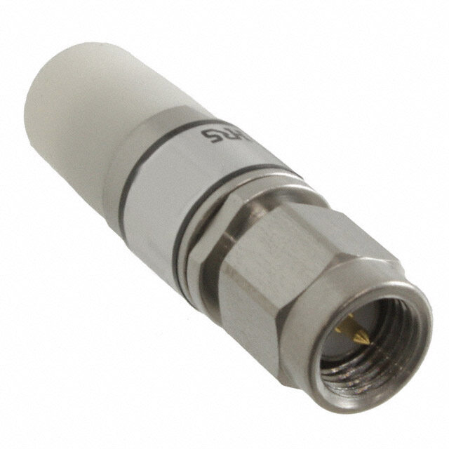
ICGOO在线商城 > 射频/IF 和 RFID > 衰减器 > AT-107-PIN
- 型号: AT-107-PIN
- 制造商: M/A-COM
- 库位|库存: xxxx|xxxx
- 要求:
| 数量阶梯 | 香港交货 | 国内含税 |
| +xxxx | $xxxx | ¥xxxx |
查看当月历史价格
查看今年历史价格
AT-107-PIN产品简介:
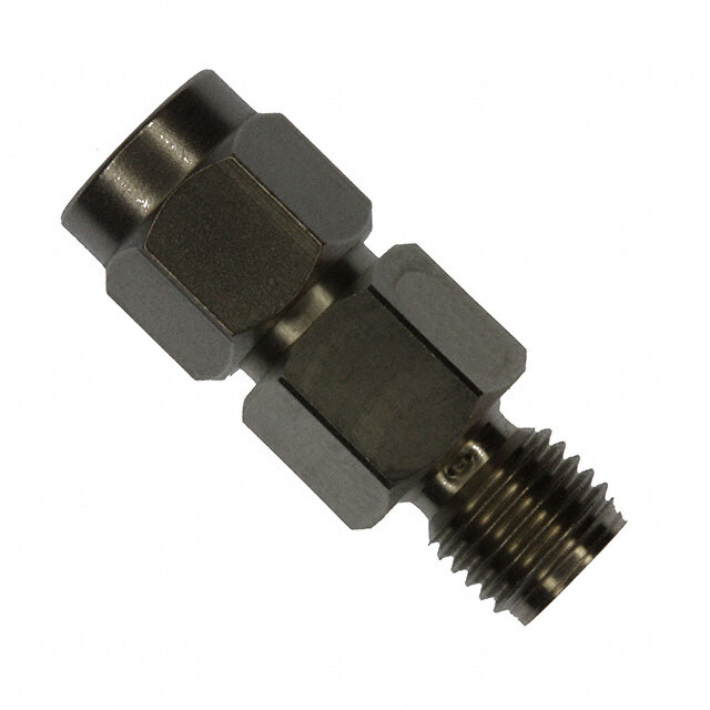
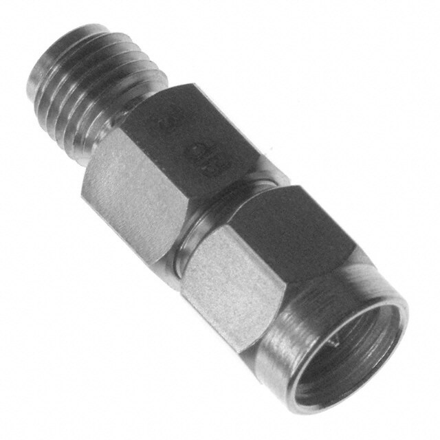
ICGOO电子元器件商城为您提供AT-107-PIN由M/A-COM设计生产,在icgoo商城现货销售,并且可以通过原厂、代理商等渠道进行代购。 AT-107-PIN价格参考¥1857.70-¥1950.47。M/A-COMAT-107-PIN封装/规格:衰减器, RF Attenuator 31.5dB ±0.4dB 0Hz ~ 2GHz 50 Ohms CR-13。您可以下载AT-107-PIN参考资料、Datasheet数据手册功能说明书,资料中有AT-107-PIN 详细功能的应用电路图电压和使用方法及教程。
| 参数 | 数值 |
| 产品目录 | |
| 描述 | ATTENUATOR RF DIGITAL有源衰减器 DC-2.0GHz 6-bit Atten=5dB to 31.5dB |
| 产品分类 | |
| 品牌 | M/A-Com Technology SolutionsMACOM |
| 产品手册 | |
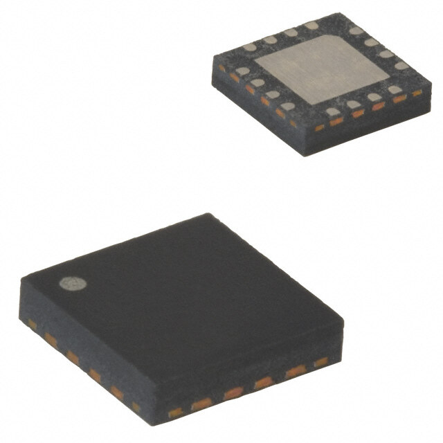
| 产品图片 |
|
| 产品系列 | RF集成电路,有源衰减器,MACOM AT-107-PIN- |
| 数据手册 | |
| 产品型号 | AT-107-PINAT-107-PIN |
| rohs | 无铅 / 符合限制有害物质指令(RoHS)规范要求 |
| 产品种类 | 有源衰减器 |
| 位数 | 6 bit |
| 其它名称 | 1465-1003 |
| 功率(W) | - |
| 商标 | MACOM |
| 容差 | ±0.4dB |
| 封装 | Bulk |
| 封装/外壳 | CR-13 |
| 封装/箱体 | CR-13-24 |
| 最大VSWR | 1.8:1 |
| 最大工作温度 | + 85 C |
| 最大衰减 | 31.5 dB |
| 最大频率 | 2 GHz |
| 最小工作温度 | - 55 C |
| 最小频率 | 0 MHz |
| 标准包装 | 25 |
| 衰减值 | 31.5dB |
| 通道数量 | 1 Channel |
| 阻抗 | 50 Ohms50 欧姆 |
| 频率范围 | 0 ~ 2GHz |



-PJ.jpg)


- 商务部:美国ITC正式对集成电路等产品启动337调查
- 曝三星4nm工艺存在良率问题 高通将骁龙8 Gen1或转产台积电
- 太阳诱电将投资9.5亿元在常州建新厂生产MLCC 预计2023年完工
- 英特尔发布欧洲新工厂建设计划 深化IDM 2.0 战略
- 台积电先进制程称霸业界 有大客户加持明年业绩稳了
- 达到5530亿美元!SIA预计今年全球半导体销售额将创下新高
- 英特尔拟将自动驾驶子公司Mobileye上市 估值或超500亿美元
- 三星加码芯片和SET,合并消费电子和移动部门,撤换高东真等 CEO
- 三星电子宣布重大人事变动 还合并消费电子和移动部门
- 海关总署:前11个月进口集成电路产品价值2.52万亿元 增长14.8%




PDF Datasheet 数据手册内容提取
AT-107-PIN Digital Attenuator 31.5 dB, 6-Bit, TTL Driver, DC-2.0 GHz Rev. V9 Features Functional Schematic Attenuation: 0.5 dB steps to 31.5 dB Temperature Stability: ± 0.18 dB from –55°C to PIN 1 GND RF1 PIN 24 +85°C Typical GND 16 dB GND Low DC Power Consumption GND GND Hermetic Surface Mount Package 8 dB Integral TTL Driver C16 GND 50 Ohm Nominal Impedance C8 GND 4 dB Lead-Free CR-13 Package Vee (-5V to -8V) GND 260°C Reflow Compatible Vcc (+5V) GND 2 dB RoHS* Compliant C4 GND C2 1 dB GND Description C1 GND Orientation Mark C0.5 0.5 dB GND M/A-COM’s AT-107-PIN is a GaAs FET 6-bit digital PIN 12 GND RF2 PIN 13 attenuator with a 0.5 dB minimum step size and 31.5 dB total attenuation. This attenuator and integral TTL driver is in a hermetically sealed ceramic 24- lead surface mount package. The AT-107-PIN is ideally suited for use where accuracy, fast switching, very low power consumption and low intermodula- Pin Configuration tion products are required. Typical applications in- clude dynamic range setting in precision receiver Pin No. Function Pin No. Function circuits and other gain/leveling control circuits. Envi- ronmental screening is available. Contact the fac- 1 GND 13 RF2 tory for information. 2 GND 14 GND 3 GND 15 GND 4 C16 16 GND 5 C8 17 GND Ordering Information 6 Vee (-5V to -8V) 18 GND 7 Vcc (+5V) 19 GND Part Number Package 8 C4 20 GND 9 C2 21 GND AT-107-PIN Bulk Packaging 10 C1 22 GND AT-107-TB Sample Test Board 11 C0.5 23 GND Note: Reference Application Note M513 for reel size 12 GND 24 RF1 information. The metal bottom of the case must be connected to RF and DC ground. * Restrictions on Hazardous Substances, European Union Directive 2011/65/EU. 111 M/A-COM Technology Solutions Inc. (MACOM) and its affiliates reserve the right to make changes to the product(s) or information contained herein without notice. Visit www.macom.com for additional data sheets and product information. For further information and support please visit: https://www.macom.com/support
AT-107-PIN Digital Attenuator 31.5 dB, 6-Bit, TTL Driver, DC-2.0 GHz Rev. V9 Electrical Specifications: T = -55°C to +85°C 1 A Parameter Test Conditions Frequency Units Min Typ Max Reference Insertion Loss — DC - 0.5 GHz dB — — 3.2 DC - 1.0 GHz dB — — 3.6 DC - 2.0 GHz dB — — 4.0 Attenuation Accuracy 2 Any Single Bit DC - 1.0 GHz ± (0.15 +3% of atten. setting in dB) dB DC - 2.0 GHz ± (0.2 +3% of atten. setting in dB) dB Any Combination of Bits DC - 1.0 GHz ± (0.2 +3% of atten. setting in dB) dB or ± 0.4 dB, whichever is greater DC - 2.0 GHz ± (0.2 +3% of atten. setting in dB) dB or ± 0.4 dB, whichever is greater VSWR — DC - 2.0 GHz Ratio — — 1.8:1 Trise, Tfall 10% to 90% — ns — 9 — Ton, Toff 50% Control to 90/10% RF — ns — 45 — Transients In-Band (peak-peak) — mV — 40 — 1 dB Compression Input Power 0.05 GHz dBm — +21 — Input Power 0.5 - 2.0 GHz dBm — +29 — Input IP3 For two-tone Input Power 0.05 GHz dBm — +35 — Up to +5 dBm 0.5 - 2.0 GHz dBm — +48 — Input IP2 For two-tone Input Power 0.05 GHz dBm — +45 — Up to +5 dBm 0.5 - 2.0 GHz dBm — +79 — Vcc — — V 4.5 5.0 5.5 Vee — — V -8.0 — -5.0 Icc Vcc = 4.5 to 5.5V — mA — — 6.0 Vctl = 0 to 0.8V, or Vcc – 2.1V to Vcc Iee Vee = -5.0 to -8.0V — mA — — 1.0 Vctl Logic 0 (TTL) — V 0.0 — 0.8 Vctl Logic 1 (TTL) — V 2.0 — 5.0 Input Leakage Current (Low) 0 to 0.8V — µA — — 1.0 Input Leakage Current (High) 2.0 to 5.0V — µA — — 1.0 1. All specifications apply when operated with bias voltages of +5V for Vcc and –5.0V for Vee. 2. This attenuator is guaranteed monotonic. 222 M/A-COM Technology Solutions Inc. (MACOM) and its affiliates reserve the right to make changes to the product(s) or information contained herein without notice. Visit www.macom.com for additional data sheets and product information. For further information and support please visit: https://www.macom.com/support
AT-107-PIN Digital Attenuator 31.5 dB, 6-Bit, TTL Driver, DC-2.0 GHz Rev. V9 Recommended PCB Configuration Absolute Maximum Ratings 3,4 Parameter Absolute Maximum Max Input Power 0.05 GHz +27 dBm 0.5 - 2.0 GHz +34 dBm V -0.5V ≤ V ≤ +7.0V CC CC V -8.5V ≤ V ≤ +0.5V EE EE V - V -0.5V ≤ V - V ≤ 14.5V CC EE CC EE Vin5 -0.5V ≤ Vin ≤ V + 0.5V CC Operating Temperature -55°C to +125°C Storage Temperature -65°C to +150°C 3. Exceeding any one or combination of these limits may cause permanent damage to this device. 4. M/A-COM does not recommend sustained operation near these survivability limits. 5. Standard CMOS TTL interface, latch-up will occur if logic Truth Table (Digital Attenuator) signal is applied prior to power supply. Control Inputs Handling Procedures C6 C5 C4 C3 C2 C1 Attenuation Please observe the following precautions to avoid 0 0 0 0 0 0 Reference damage: 0 0 0 0 0 1 0.5 dB Static Sensitivity 0 0 0 0 1 0 1 dB Gallium Arsenide Integrated Circuits are sensitive 0 0 0 1 0 0 2 dB to electrostatic discharge (ESD) and can be 0 0 1 0 0 0 4 dB damaged by static electricity. Proper ESD control 0 1 0 0 0 0 8 dB techniques should be used when handling these devices. 1 0 0 0 0 0 16 dB 1 1 1 1 1 1 31.5 dB Typical Performance Curves 0 = TTL Low; 1 = TTL High Insertion Loss vs. Frequency Attenuation Accuracy vs. Frequency +85°C +25°C -55°C n 1 dB 4 dB 2 dB 0.5 dB 5.0 e 0.60 Att B) 4.0 nal 0.40 oss (d 3.0 Nomi 0.20 L m B) Insertion 21..00 ation fro (d-00..2000 vi -0.40 e D 0.0 -0.60 0.0 0.5 1.0 1.5 2.0 0.0 0.5 1.0 1.5 2.0 Frequency (GHz) Frequency (GHz) 333 M/A-COM Technology Solutions Inc. (MACOM) and its affiliates reserve the right to make changes to the product(s) or information contained herein without notice. Visit www.macom.com for additional data sheets and product information. For further information and support please visit: https://www.macom.com/support
AT-107-PIN Digital Attenuator 31.5 dB, 6-Bit, TTL Driver, DC-2.0 GHz Rev. V9 Typical Performance Curves Attenuation Accuracy vs. Frequency RF1 VSWR vs. Frequency 8 dB 16 dB 31.5 dB 1 dB 4 dB 8 & 16 dB Ref Loss & 0.5 dB n e 0.80 2 Att minal 0.40 1.8 o N R 1.6 m B) W n fro (d0.00 VS 1.4 o ti -0.40 a 1.2 vi e D -0.80 1 0.0 0.5 1.0 1.5 2.0 0.0 0.5 1.0 1.5 2.0 Frequency (GHz) Frequency (GHz) RF2 VSWR vs. Frequency Lead-Free, CR-13 Ceramic Package† 1 & 2 dB 4 dB 8 dB 16 dB Ref Loss & 0.5 dB 2 1.8 R 1.6 W S V1.4 1.2 1 0.0 0.5 1.0 1.5 2.0 Frequency (GHz) † Reference Application Note M538 for lead-free solder reflow recommendations. 444 M/A-COM Technology Solutions Inc. (MACOM) and its affiliates reserve the right to make changes to the product(s) or information contained herein without notice. Visit www.macom.com for additional data sheets and product information. For further information and support please visit: https://www.macom.com/support
AT-107-PIN Digital Attenuator 31.5 dB, 6-Bit, TTL Driver, DC-2.0 GHz Rev. V9 M/A-COM Technology Solutions Inc. All rights reserved. Information in this document is provided in connection with M/A-COM Technology Solutions Inc ("MACOM") products. These materials are provided by MACOM as a service to its customers and may be used for informational purposes only. Except as provided in MACOM's Terms and Conditions of Sale for such products or in any separate agreement related to this document, MACOM assumes no liability whatsoever. MACOM assumes no responsibility for errors or omissions in these materials. MACOM may make changes to specifications and product descriptions at any time, without notice. MACOM makes no commitment to update the information and shall have no responsibility whatsoever for conflicts or incompatibilities arising from future changes to its specifications and product descriptions. No license, express or implied, by estoppels or otherwise, to any intellectual property rights is granted by this document. THESE MATERIALS ARE PROVIDED "AS IS" WITHOUT WARRANTY OF ANY KIND, EITHER EXPRESS OR IMPLIED, RELATING TO SALE AND/OR USE OF MACOM PRODUCTS INCLUDING LIABILITY OR WARRANTIES RELATING TO FITNESS FOR A PARTICULAR PURPOSE, CONSEQUENTIAL OR INCIDENTAL DAMAGES, MERCHANTABILITY, OR INFRINGEMENT OF ANY PATENT, COPYRIGHT OR OTHER INTELLECTUAL PROPERTY RIGHT. MACOM FURTHER DOES NOT WARRANT THE ACCURACY OR COMPLETENESS OF THE INFORMATION, TEXT, GRAPHICS OR OTHER ITEMS CONTAINED WITHIN THESE MATERIALS. MACOM SHALL NOT BE LIABLE FOR ANY SPECIAL, INDIRECT, INCIDENTAL, OR CONSEQUENTIAL DAMAGES, INCLUDING WITHOUT LIMITATION, LOST REVENUES OR LOST PROFITS, WHICH MAY RESULT FROM THE USE OF THESE MATERIALS. MACOM products are not intended for use in medical, lifesaving or life sustaining applications. MACOM customers using or selling MACOM products for use in such applications do so at their own risk and agree to fully indemnify MACOM for any damages resulting from such improper use or sale. 555 M/A-COM Technology Solutions Inc. (MACOM) and its affiliates reserve the right to make changes to the product(s) or information contained herein without notice. Visit www.macom.com for additional data sheets and product information. For further information and support please visit: https://www.macom.com/support

 Datasheet下载

