- 型号: AS5311-ATSU
- 制造商: AUSTRIAMICROSYSTEMS
- 库位|库存: xxxx|xxxx
- 要求:
| 数量阶梯 | 香港交货 | 国内含税 |
| +xxxx | $xxxx | ¥xxxx |
查看当月历史价格
查看今年历史价格
AS5311-ATSU产品简介:
ICGOO电子元器件商城为您提供AS5311-ATSU由AUSTRIAMICROSYSTEMS设计生产,在icgoo商城现货销售,并且可以通过原厂、代理商等渠道进行代购。 AS5311-ATSU价格参考。AUSTRIAMICROSYSTEMSAS5311-ATSU封装/规格:编码器, 。您可以下载AS5311-ATSU参考资料、Datasheet数据手册功能说明书,资料中有AS5311-ATSU 详细功能的应用电路图电压和使用方法及教程。
AMS(艾迈斯)的AS5311-ATSU是一款高精度的角度传感器,广泛应用于需要精确角度测量和位置反馈的各种工业和消费类设备中。以下是其主要应用场景:

 1. 工业自动化
   AS5311-ATSU在工业自动化领域中常用于电机控制、机器人关节、伺服系统等设备中。它能够提供高精度的角度反馈,确保机械臂、传送带等设备的运动更加精准和平稳。例如,在工厂自动化生产线中,该传感器可以实时监测机械臂的旋转角度,确保每个动作都符合预设参数,从而提高生产效率和产品质量。

 2. 汽车电子
   在汽车行业中,AS5311-ATSU可用于转向系统、电动助力转向(EPS)、座椅调节、天窗开合等场景。它能够精确检测转动部件的角度变化,确保车辆的安全性和舒适性。例如,在EPS系统中,传感器可以实时监测方向盘的角度变化,帮助车辆实现更灵敏的转向响应,提升驾驶体验。

 3. 智能家居与家电
   在智能家居和家电领域,AS5311-ATSU可以应用于智能锁、自动门、窗帘控制器等设备中。它能够精确感知门锁或窗户的开合状态,确保设备的正常运行。此外,在智能家电如洗碗机、洗衣机等设备中,传感器可以监控内部部件的旋转角度,确保设备的高效运行。

 4. 医疗设备
   医疗设备对精度要求极高,AS5311-ATSU凭借其高分辨率和可靠性,适用于手术机器人、康复设备、呼吸机等医疗设备中。它可以精确测量关节的旋转角度,帮助医生进行更精细的操作,确保患者的安全和治疗效果。

 5. 无人机与航空航天
   在无人机和航空航天领域,AS5311-ATSU可以用于姿态控制、飞行器舵面角度检测等场景。它能够实时监测飞行器的姿态变化,确保飞行的稳定性和安全性。例如,在无人机的飞行控制系统中,传感器可以精确检测螺旋桨的转速和角度,帮助无人机保持平衡并执行复杂的飞行任务。

总之,AS5311-ATSU凭借其高精度、可靠性和低功耗的特点,广泛应用于多个领域,为各种设备提供了精确的角度测量和位置反馈功能。
| 参数 | 数值 |
| 产品目录 | |
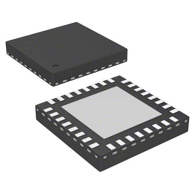
| 描述 | IC ENCODER LINEAR 20-TSSOP板机接口霍耳效应/磁性传感器 Linear incremental position sensor |
| 产品分类 | 磁性传感器 - 霍尔效应,数字开关,线性,罗盘 (IC)磁性传感器 |
| 品牌 | ams |
| 产品手册 | http://ams.com/eng/content/download/17954/325059/15366 |
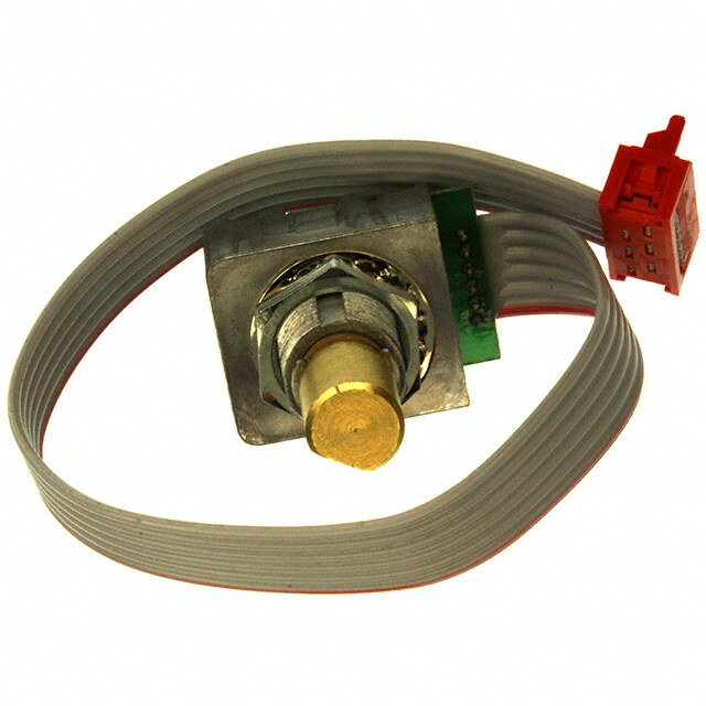
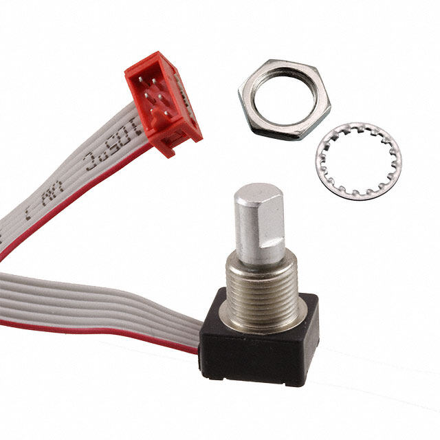
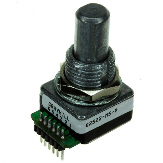
| 产品图片 |
|
| rohs | 符合RoHS无铅 / 符合限制有害物质指令(RoHS)规范要求 |
| 产品系列 | 板机接口霍耳效应/磁性传感器,ams AS5311-ATSU- |
| 数据手册 | http://www.ams.com/eng/content/view/download/79194http://www.ams.com/eng/content/download/17954/325059/15366 |
| 产品型号 | AS5311-ATSU |
| 产品培训模块 | http://www.digikey.cn/PTM/IndividualPTM.page?site=cn&lang=zhs&ptm=25346 |
| 产品种类 | 板机接口霍耳效应/磁性传感器 |
| 供应商器件封装 | 20-TSSOP |
| 其它名称 | AS5311-ASSU |
| 包装 | 管件 |
| 商标 | ams |
| 安装风格 | SMD/SMT |
| 封装 | Tube |
| 封装/外壳 | 20-TSSOP(0.173",4.40mm 宽) |
| 封装/箱体 | TSSOP-20 |
| 工作温度 | -40°C ~ 125°C |
| 工作电源电压 | 3.3 V to 5 V |
| 工厂包装数量 | 74 |
| 应用说明 | http://www.austriamicrosystems.com/eng/content/view/download/11922http://www.austriamicrosystems.com/eng/content/view/download/11921 |
| 感应范围 | 10mT ~ 40mT |
| 最大工作温度 | + 125 C |
| 最大输出电流 | 4 mA |
| 最小/最大释放点(Brp) | 10 mT to 40 mT |
| 标准包装 | 74 |
| 特性 | - |
| 电压-电源 | 3 V ~ 3.6 V,4.5 V ~ 5.5 V |
| 电流-电源 | 21mA |
| 电流-输出(最大值) | 4mA |
| 电源电流 | 21 mA |
| 类型 | Absolute Encoders |
| 输出类型 | 数字式,PWM,12 位串行 |





- 商务部:美国ITC正式对集成电路等产品启动337调查
- 曝三星4nm工艺存在良率问题 高通将骁龙8 Gen1或转产台积电
- 太阳诱电将投资9.5亿元在常州建新厂生产MLCC 预计2023年完工
- 英特尔发布欧洲新工厂建设计划 深化IDM 2.0 战略
- 台积电先进制程称霸业界 有大客户加持明年业绩稳了
- 达到5530亿美元!SIA预计今年全球半导体销售额将创下新高
- 英特尔拟将自动驾驶子公司Mobileye上市 估值或超500亿美元
- 三星加码芯片和SET,合并消费电子和移动部门,撤换高东真等 CEO
- 三星电子宣布重大人事变动 还合并消费电子和移动部门
- 海关总署:前11个月进口集成电路产品价值2.52万亿元 增长14.8%


PDF Datasheet 数据手册内容提取
AS5311 High Resolution Magnetic Linear Encoder 1 General Description The AS5311 is available in a PB-free TSSOP-20 package and qualified for an ambient temperature range from -40°C to +125°C. The AS5311 is a contactless high resolution magnetic linear encoder for accurate linear motion and off-axis rotary sensing with a 2 Key Features resolution down to <0.5µm. It is a system-on-chip, combining integrated Hall elements, analog front end and digital signal processing on a single chip, packaged in a small 20-pin TSSOP Two 12-bit digital absolute outputs: package. - Serial interface and A multi-pole magnetic strip or ring with a pole length of 1.0mm is - Pulse width modulated (PWM) output required to sense the rotational or linear motion. The magnetic strip Incremental output with Index is placed above the IC at a distance of typ. 0.3mm. “Red-Yellow-Green” indicators monitor magnet placement over The absolute measurement provides instant indication of the magnet the chip position within one pole pair with a resolution of 488nm per step (12- bit over 2.0mm). This digital data is available as a serial bit stream 3 Applications and as a PWM signal. Furthermore, an incremental output is available with a resolution of Micro-Actuator feedback 1.95µm per step. An index pulse is generated once for every pole Servo drive feedback pair (once per 2.0mm).The travelling speed in incremental mode is up to 650mm/second. Robotics An internal voltage regulator allows the AS5311 to operate at either Replacement of optical encoders 3.3 V or 5 V supplies. Depending on the application the AS5311 accepts multi-pole strip magnets as well as multi-pole ring magnets, both radial and axial magnetized (see Figure1 and Figure3). Figure 1. AS5311 Block Diagram VDD3V3 MagINCn VDD5V LDO 3.3V MagDECn PWM PWM Interface Sin Ang Linear Hall DSP Absolute DO Array Cos Mag Interface CSn & (SSI) Frontend CLK Amplifier OTP Register A Incremental Programming Interface B AS5311 Parameters Index Prog www.ams.com/AS5311 Revision 1.13 1 - 32
AS5311 Datasheet - Contents Contents 1 General Description.................................................................................................................................................................. 1 2 Key Features............................................................................................................................................................................. 1 3 Applications............................................................................................................................................................................... 1 4 Pin Assignments....................................................................................................................................................................... 3 4.1 Pin Descriptions.................................................................................................................................................................................... 3 5 Absolute Maximum Ratings...................................................................................................................................................... 5 6 Electrical Characteristics........................................................................................................................................................... 6 6.1 Operating Conditions............................................................................................................................................................................ 6 6.2 DC Characteristics for Digital Inputs and Outputs................................................................................................................................ 6 6.2.1 CMOS Schmitt-Trigger Inputs: CLK, CSn (CSn = internal Pull-up)............................................................................................. 6 6.2.2 CMOS Output Open Drain: MagINCn, MagDECn....................................................................................................................... 6 6.2.3 CMOS Output: PWM................................................................................................................................................................... 6 6.2.4 Tristate CMOS Output: DO.......................................................................................................................................................... 7 6.3 Magnetic Input Specification................................................................................................................................................................. 7 6.4 Electrical System Specifications........................................................................................................................................................... 8 6.5 Timing Characteristics.......................................................................................................................................................................... 9 6.5.1 Pulse Width Modulation Output................................................................................................................................................... 9 7 Detailed Description................................................................................................................................................................ 10 7.1 Incremental Outputs........................................................................................................................................................................... 11 7.1.1 Incremental Power-up Lock Option........................................................................................................................................... 11 7.2 Incremental Output Hysteresis........................................................................................................................................................... 12 7.3 Synchronous Serial Interface (SSI).................................................................................................................................................... 12 7.4 Absolute Output Jitter and Hysteresis................................................................................................................................................ 14 7.4.1 Adding a Digital Hysteresis........................................................................................................................................................ 14 7.4.2 Implementing Digital Filtering.................................................................................................................................................... 14 7.5 Z-axis Range Indication (“Red/Yellow/Green” Indicator).................................................................................................................... 14 7.6 Pulse Width Modulation (PWM) Output.............................................................................................................................................. 15 7.7 3.3V / 5V Operation............................................................................................................................................................................ 16 8 Application Information........................................................................................................................................................... 18 8.1 Magnetization..................................................................................................................................................................................... 19 8.2 Position of the Index Pulse................................................................................................................................................................. 19 8.3 Mounting the Magnet.......................................................................................................................................................................... 19 8.3.1 Vertical Distance........................................................................................................................................................................ 19 8.3.2 Alignment of Multi-pole Magnet and IC...................................................................................................................................... 20 8.3.3 Lateral Stroke of Multi-pole Strip Magnets................................................................................................................................. 20 8.4 Measurement Data Example.............................................................................................................................................................. 22 8.5 AS5311 Off-axis Rotary Applications.................................................................................................................................................. 23 8.6 Programming the AS5311.................................................................................................................................................................. 25 8.6.1 Zero Position Programming....................................................................................................................................................... 25 8.6.2 User Selectable Settings........................................................................................................................................................... 26 9 Package Drawings and Markings........................................................................................................................................... 28 9.1 Recommended PCB Footprint............................................................................................................................................................ 29 10 Ordering Information............................................................................................................................................................. 31 www.ams.com/AS5311 Revision 1.13 2 - 32
AS5311 Datasheet - Pin Assignments 4 Pin Assignments Figure 2. Pin Assignments (Top View) NC 1 20 NC MagIncn 2 19 VDD5V MagDecn 3 18 VDD3V3 A 4 17 NC 1 1 B 5 53 16 NC S NC 6 A 15 PWM Index 7 14 CSn VSS 8 13 CLK Prog 9 12 DO NC 10 11 NC 4.1 Pin Descriptions Pin 4(A), 5(B) and 7(Index) are the incremental outputs. The incremental output has a resolution of 10-bit per pole pair, resulting in a step length of 1.95µm. Note: Pin 14 (CSn) must be low to enable the incremental outputs. Pins 12, 13 and 14 are used for serial data transfer. Chip Select (CSn; active low) initiates serial data transfer. CLK is the clock input and DO is the data output. A logic high at CSn puts the data output pin (DO) to tri-state and terminates serial data transfer. CSn must be low to enable the incremental outputs. See Section 7.1.1 for further options. Pin 8 is the supply ground pin. Pins 18 and 19 are the positive supply pins. For 5V operation, connect the 5V supply to pin 19 and add a 2µF…10µF buffer capacitor at pin 18. For 3.3V operation, connect both pins 18 and 19 to the 3.3V supply. Pin 9 is used for factory programming only. It should be connected to VSS. Pins 2 and 3 are the magnetic field change indicators, MagINCn and MagDECn (magnetic field strength increase or decrease through variation of the distance between the magnet and the device). These outputs can be used to detect the valid magnetic field range. External pull-up resistors are required at these pins. See Section 6.2.2 for maximum output currents on these pins. Since they are open-drain outputs they can also be combined (wired-and). Pin 15 (PWM) allows a single wire output of the 12-bit absolute position value within one pole pair (2.0mm). The value is encoded into a pulse width modulated signal with 1µs pulse width per step (1µs to 4097µs over one pole pair). Pins 1, 6, 10, 11, 16, 17 and 20 are for internal use and must not be connected. www.ams.com/AS5311 Revision 1.13 3 - 32
AS5311 Datasheet - Pin Assignments Table 1. Pin Descriptions Pin Number Pin Name Pin Type Description 1 NC - Must be left unconnected Indicates “Red/Yellow/Green Range” depending on the distance between device 2 MagINCn and magnet Digital output open drain Indicates “Red/Yellow/Green Range” depending on the distance between device 3 MagDECn and magnet 4 A Incremental output A Digital output 5 B Incremental output B 6 NC - Must be left unconnected 7 Index Digital output Incremental output Index 8 VSS Supply pin Negative Supply Voltage (GND) 9 Prog Digital input pull-down OTP Programming Input for factory programming. Connect to VSS. 10 NC - Must be left unconnected 11 NC - Must be left unconnected 12 DO Digital output /tri-state Data Output of Synchronous Serial Interface Digital input, 13 CLK Clock Input of Synchronous Serial Interface; Schmitt-Trigger input Schmitt-Trigger input Digital input pull-up, Chip Select, active low; Schmitt-Trigger input, internal pull-up resistor (~50kW). 14 CSn Schmitt-Trigger input Must be low to enable incremental outputs 15 PWM Digital output Pulse Width Modulation of approx. 244Hz; 1µs/step 16 NC - Must be left unconnected 17 NC - Must be left unconnected 3V-Regulator output; internally regulated from VDD5V. 18 VDD3V3 Supply pin Connect to VDD5V for 3V supply voltage. Do not load externally. 19 VDD5V Positive Supply Voltage, 3.0 to 5.5 V 20 NC - Must be left unconnected www.ams.com/AS5311 Revision 1.13 4 - 32
AS5311 Datasheet - Absolute Maximum Ratings 5 Absolute Maximum Ratings Stresses beyond those listed in Table 2 may cause permanent damage to the device. These are stress ratings only, and functional operation of the device at these or any other conditions beyond those indicated in Electrical System Specifications on page 8 is not implied. Exposure to absolute maximum rating conditions for extended periods may affect device reliability. Table 2. Absolute Maximum Ratings Parameter Min Max Units Comments DC supply voltage at pin VDD5V -0.3 7 V DC supply voltage at pin VDD3V3 5 V VDD5V Input pin voltage -0.3 V Except VDD3V3 +0.3 Input current (latchup immunity) -100 100 mA Norm: JEDEC 78 Electrostatic discharge ± 2 kV Norm: MIL 883 E method 3015 Storage temperature -55 125 °C Min – 67°F; Max +257°F The reflow peak soldering temperature (body temperature) specified is in accordance with IPC/ JEDEC J-STD-020 “Moisture/Reflow Sensitivity Body temperature (Lead-free package) 260 °C Classification for Non-Hermetic Solid State Surface Mount Devices”. The lead finish for Pb-free leaded packages is matte tin (100% Sn). Humidity non-condensing 5 85 % Moisture Sensitive Level (MSL) 3 Represents a maximum floor time of 168h www.ams.com/AS5311 Revision 1.13 5 - 32
AS5311 Datasheet - Electrical Characteristics 6 Electrical Characteristics TAMB = -40 to +125°C, VDD5V = 3.0-3.6V (3V operation) VDD5V = 4.5-5.5V (5V operation), unless otherwise noted. 6.1 Operating Conditions Table 3. Operating Conditions Symbol Parameter Note Min Typ Max Units TAMB Ambient temperature -40°F +257°F -40 125 °C Isupp Supply current 16 21 mA Supply voltage at pin VDD5V VDD5V 4.5 5.0 5.5 V Voltage regulator output voltage at pin 5V Operation VDD3V3 3.0 3.3 3.6 V VDD3V3 VDD5V Supply voltage at pin VDD5V 3.3V Operation 3.0 3.3 3.6 V VDD3V3 Supply voltage at pin VDD3V3 (pin VDD5V and VDD3V3 connected) 3.0 3.3 3.6 V 6.2 DC Characteristics for Digital Inputs and Outputs 6.2.1 CMOS Schmitt-Trigger Inputs: CLK, CSn (CSn = internal Pull-up) Table 4. CMOS Schmitt-Trigger Inputs Symbol Parameter Conditions Min Typ Max Units VIH High level input voltage Normal operation 0.41 * VDD5V V VIL Low level input voltage 0.13 * VDD5V V VIon - VIoff Schmitt Trigger hysteresis 1 V ILEAK Input leakage current CLK only -1 1 µA IiL Pull-up low level input current CSn only, VDD5V: 5.0V -30 -100 6.2.2 CMOS Output Open Drain: MagINCn, MagDECn Table 5. CMOS Output Open Drain Symbol Parameter Conditions Min Typ Max Units VOL Low level output voltage VSS+0.4 V VDD5V: 4.5V 4 IO Output current mA VDD5V: 3V 2 IOZ Open drain leakage current 1 µA 6.2.3 CMOS Output: PWM Table 6. CMOS Output Symbol Parameter Conditions Min Typ Max Units VOH High level output voltage VDD5V-0.5 V VOL Low level output voltage VSS+0.4 V VDD5V: 4.5V 4 IO Output current mA VDD5V: 3V 2 www.ams.com/AS5311 Revision 1.13 6 - 32
AS5311 Datasheet - Electrical Characteristics 6.2.4 Tristate CMOS Output: DO Table 7. Tristate CMOS Output Symbol Parameter Conditions Min Typ Max Units VOH High level output voltage VDD5V -0.5 V VOL Low level output voltage VSS+0.4 V VDD5V: 4.5V 4 IO Output current mA VDD5V: 3V 2 6.3 Magnetic Input Specification Two-pole cylindrical diametrically magnetized source: Table 8. Magnetic Input Specification Symbol Parameter Note Min Typ Max Units Lp Pole length Recommended magnet: plastic or rubber 1 mm bonded ferrite or NdFeB tmag Pole pair length 2 mm Required vertical component of the Bpk Magnetic input field amplitude magnetic field strength on the die’s surface 10 40 mT Boff Magnetic offset Constant magnetic stray field ± 5 mT Recommended magnet: plastic or rubber Btc Magnetic field temperature drift bonded ferrite or NdFeB 0.2 %/K Magnetic input field variation Including offset gradient ±2 % Incremental output: 1024 steps / polepair mm/ Vabs Linear travelling speed including interpolation1 650 sec Maximum shift between defined Hall sensor Disp Displacement center and magnet centerline; depends on 0.5 mm magnet geometries Package to magnet surface; ZDist Vertical gap depends on magnet strength 0.3 mm Plastic or rubber bonded Ferrite -0.19 Recommended magnet material and %/K temperature drift Plastic or rubber bonded Neodymium -0.12 (NdFeB) 1. 1) For absolute outputs, a practical speed limit is 2345 mm/s. At higher speeds, input signal cancellation will occur and the detected field decreases due to the internal front-end. Significant signal change is indicated by the status bits. 2) With increasing speed, the distance between two samples increases. The travelling distance between two subsequent samples can be calculated as: v sampling–dist = ---- fs where: sampling_distance = travelling distance between samples (in mm) v = travelling speed (in mm/sec) fs = sampling rate in Hz (see Table 9) www.ams.com/AS5311 Revision 1.13 7 - 32
AS5311 Datasheet - Electrical Characteristics 6.4 Electrical System Specifications Table 9. Electrical System Specifications Symbol Parameter Note Min Typ Max Units bit / RESabs Resolution, absolute outputs 0.488 um/step (12bit / 2mm pole pair) 12 polepair bit / RESinc Resolution, incremental outputs 1.95 um/step (10bit / 2mm pole pair) 10 polepair Maximum error with respect to the best line INLopt Integral non-linearity (optimum) fit. Ideal magnet ± 5.6 μm TAMB =25 °C. Maximum error with respect to the best line Integral non-linearity (over INLtemp temperature) fit. Ideal magnet ± 10 μm Tamb = -30 to +70 °C. DNL Differential non-linearity 10bit, no missing codes ± 0.97 μm TN Transition noise 1 sigma 0.6 μm RMS Power-on reset thresholds: Von On voltage; 300mV typ. hysteresis 1.37 2.2 2.9 DC supply voltage 3.3V (VDD3V3) V Power-on reset thresholds: Voff Off voltage; 300mV typ. hysteresis 1.08 1.9 2.6 tPwrUp Power-up time Until status bit OCF = 1 20 ms System propagation delay absolute tdelay output Delay of ADC, DSP and absolute interface 96 µs System propagation delay incremental tdelay output Including interpolation delay at high speeds 384 µs Internal sampling rate for absolute TAMB = 25°C 9.90 10.42 10.94 fS output kHz TAMB = -40 to +125°C, 9.38 10.42 11.46 Hyst Hysteresis, incremental outputs No Hysteresis at absolute serial outputs 2 LSB Maximum clock frequency to read out serial CLK Read-out frequency 1 MHz data Notes: 1. Integral Non-Linearity (INL) is the maximum deviation between actual position and indicated position. 2. Differential Non-Linearity (DNL) is the maximum deviation of the step length from one position to the next. 3. Transition Noise (TN) is the repeatability of an indicated position. www.ams.com/AS5311 Revision 1.13 8 - 32
AS5311 Datasheet - Electrical Characteristics 6.5 Timing Characteristics Table 10. Synchronous Serial Interface (SSI) Symbol Parameter Note Min Typ Max Units Time between falling edge of CSn and data tDOactive Data output activated (logic high) output activated 100 ns Time between falling edge of CSn and first tCLKFE First data shifted to output register falling edge of CLK 500 ns TCLK / 2 Start of data output Rising edge of CLK shifts out one bit at a time 500 ns Time between rising edge of CLK and data tDOvalid Data output valid output valid 413 ns tDOtristate Data output tristate After the last bit DO changes back to “tristate” 100 ns CSn = high; To initiate read-out of next angular tCSn Pulse width of CSn position 500 ns fCLK Read-out frequency Clock frequency to read out serial data >0 1 MHz 6.5.1 Pulse Width Modulation Output Table 11. Pulse Width Modulation Output Symbol Parameter Note Min Typ Max Units Signal period = 4098µs ±5% at 232 244 256 TAMB = 25°C f PWM PWM frequency Hz Signal period = 4098µs ±10% at 220 244 268 TAMB = -40 to +125°C PW MIN Minimum pulse width Position 0d = 0µm 0.9 1 1.1 µs PW MAX Maximum pulse width Position 4095d = 1999.5µm 3892 4097 4301 µs www.ams.com/AS5311 Revision 1.13 9 - 32
AS5311 Datasheet - Detailed Description 7 Detailed Description The different types of outputs relative to the magnet position are outlined in Figure3 below. The absolute serial output counts from 0….4095 within one pole pair and repeats with each subsequent pole pair. Likewise, the PWM output starts with a pulse width of 1µs, increases the pulse width with every step of 0.488µm and reaches a maximum pulse width of 4097µs at the end of each pole pair. An index pulse is generated once for every pole pair. 256 incremental pulses are generated at each output A and B for every pole pair. The outputs A and B are phase shifted by 90 electrical degrees, which results in 1024 edges per pole pair. As the incremental outputs are also repeated with every pole pair, a constant train of pulses is generated as the magnet moves over the chip. Figure 3. AS5311 Outputs Relative to Magnet Position 2mm S N S N S N S N S N S N absolute output : 0….. 4095 0….. 4095 0….. 4095 0….. 4095 0….. 4095 0….. 4095 PWM output : 1…. 4097µs A : 256 pulses / polepair B : 256 pulses / polepair A+B = 1024 steps / polepair Index : 1 pulse / polepair www.ams.com/AS5311 Revision 1.13 10 - 32
AS5311 Datasheet - Detailed Description 7.1 Incremental Outputs Figure4 shows the two-channel quadrature output of the AS5311. Output A leads output B when the magnet is moving from right to left and output B leads output A when the magnet is moving from left to right(see Figure 14). Figure 4. Incremental Outputs Mechanical Mechanical Incremental outputs Zero Position Movement Direction Zero Position Change A B Index=0 1LSB Hyst = 2 LSB Index Movement right to left Movement left to right CSn tIncremental outputs valid 7.1.1 Incremental Power-up Lock Option After power-up, the incremental outputs can optionally be locked or unlocked, depending on the status of the CSn pin: CSn = low at power-up: CSn has an internal pull-up resistor and must be externally pulled low (Rext ≤ 5kΩ). If Csn is low at power-up, the incremental outputs A, B and Index will be high until the internal offset compensation is finished. This unique state may be used as an indicator for the external controller to shorten the waiting time at power-up. Instead of waiting for the specified maximum power up-time (see Electrical System Specifications on page 8), the controller can start requesting data from the AS5311 as soon as the state (A= B= Index = high) is cleared. CSn = high or open at power-up: In this mode, the incremental outputs (A, B, Index) will remain at logic high state after power-up, until CSn goes low or a low pulse is applied at CSn and internal offset compensation is finished. This mode allows intentional disabling of the incremental outputs after power-up until for example the system microcontroller is ready to receive data. Once the incremental outputs are unlocked they can not be disabled during operation. www.ams.com/AS5311 Revision 1.13 11 - 32
AS5311 Datasheet - Detailed Description 7.2 Incremental Output Hysteresis Figure 5. Hysteresis Illustration Incremental Hysteresis: Output 2 steps Indication X +4 X +3 X +2 X +1 X Magnet Position X X +1 X +2 X +3 X +4 X +5 Movement left -->right Movement right -->left To avoid flickering incremental outputs at a stationary magnet position, a hysteresis is introduced. In case of a movement direction change, the incremental outputs have a hysteresis of 2 LSB. For constant movement directions, every magnet position change is indicated at the incremental outputs (see Figure 4). If for example the magnet moves from position “x+3” to “x+4”, the incremental output would also indicate this position accordingly. A change of the magnet’s movement direction back to position “x+3” means, that the incremental output still remains unchanged for the duration of 2 LSB, until position “x+2” is reached. Following this movement, the incremental outputs will again be updated with every change of the magnet position. 7.3 Synchronous Serial Interface (SSI) The Serial interface allows data transmission of the 12-bit absolute linear position information (within one pole pair = 2.0mm). Data bits D11:D0 represent the position information with a resolution of 488nm (2000µm / 4096) per step. CLK must be high at the falling edge of CSn. Figure 6. Synchronous Serial Interface with Absolute Angular Position Data CSn tCLK FE tCLK FE TCLK/2 tCSn CLK 1 8 18 1 DO D11 D10 D9 D8 D7 D6 D5 D4 D3 D2 D1 D0 OCF COF LIN Mag Mag Even D11 INC DEC PAR tDO active tDO valid Angular Position Data Status Bits tDO Tristate www.ams.com/AS5311 Revision 1.13 12 - 32
AS5311 Datasheet - Detailed Description If CLK is low at the falling edge of CSn, the first 12 bits represent the magnitude information, which is proportional to the magnetic field strength. This information can be used to detect the presence and proper distance of the magnetic strip by comparing it to a known good value (depends on the magnet material and distance). The automatic gain control (AGC) maintains a constant MAGnitude value of 3F hex (=“green” range). If the MAG value is <>3F hex, the AGC is out of the regulating range (“yellow” or “red” range). See Table 13 for more details. For AGC algorithm only M11: M4 of the magnitude are used. A value of zero or close to zero indicates a missing magnet. Figure 7. Synchronous Serial Interface with Magnetic Field Strength Data CSn tCLK FE TCLK/2 tCSn CLK 1 8 18 1 DO M11 M10 M9 M8 M7 M6 M5 M4 M3 M2 M1 M0 OCF COF LIN Mag Mag Even D11 INC DEC PAR tDO valid tDO active Magnetic field strength data Status Bits tDO Tristate If CSn changes to logic low, Data Out (DO) will change from high impedance (tri-state) to logic high and the read-out will be initiated. After a minimum time tCLK FE, data is latched into the output shift register with the first falling edge of CLK. Each subsequent rising CLK edge shifts out one bit of data. The serial word contains 18 bits, if CLK is high at the falling edge of CSn (see Figure 6), the first 12 bits are the absolute distance informa- tion D[11:0], the subsequent 6 bits contain system information, about the validity of data such as OCF, COF, LIN, Parity and Magnetic Field status (increase/decrease). If CLK is low at the falling edge of CSn, the first 12 bits contain the magnitude information and the subsequent bits contain the status bits (see Figure 7). A subsequent measurement is initiated by a “high” pulse at CSn with a minimum duration of tCSn. Data Contents: D11:D0 absolute linear position data (MSB is clocked out first) M11:M0 magnitude / magnetic field strength information (MSB is clocked out first) OCF (Offset Compensation Finished), logic high indicates the finished Offset Compensation Algorithm. If this bit is not set, the data at D11:D0 (likewise M11:M0) may be invalid. COF (Cordic Overflow), logic high indicates an out of range error in the CORDIC part. When this bit is set, the data at D11:D0 (likewise M11:M0) is invalid. This alarm may be resolved by bringing the magnet within the X-Y-Z tolerance limits. LIN (Linearity Alarm), logic high indicates that the input field generates a critical output linearity. When this bit is set, the data at D11:D0 may still be used, but can contain invalid data. This warning can be resolved by increasing the magnetic field strength. Even Parity bit for transmission error detection of bits 1…17 (D11…D0, OCF, COF, LIN, MagINC, MagDEC) www.ams.com/AS5311 Revision 1.13 13 - 32
AS5311 Datasheet - Detailed Description Data D11:D0 is valid, when the status bits have the following configurations: Table 12. Status Bit Outputs OCF COF LIN MagINC MagDEC Parity 0 0 0 1 1 0 0 Even checksum of bits 1:17 1 0 1* 1* *MagInc=MagDec=1 is only recommended in YELLOW mode (see Table 13). 7.4 Absolute Output Jitter and Hysteresis Note: There is no hysteresis or additional filtering at the absolute output. This allows a determination of the magnet’s absolute position within one pole pair down to submicron range. Due to the intentionally omitted hysteresis and due to noise (e.g. from weak magnetic fields), the absolute output may jitter when the magnet is stationary over the chip. In order to get a stable 12-bit absolute reading, two common methods may be implemented to reduce the jitter. 7.4.1 Adding a Digital Hysteresis The hysteresis feature of the incremental outputs is described in Incremental Output Hysteresis. An equivalent function can be implemented in the software of the external microcontroller. The hysteresis should be larger than the peak-to-peak noise (=jitter) of the absolute output in order to mask it and create a stable output reading. Note: The 2-bit hysteresis on the incremental output (=3.9µm) is equivalent to a hysteresis of 8LSB on the absolute output. 7.4.2 Implementing Digital Filtering Another useful alternative or additional method to reduce jitter is digital filtering. This can be accomplished simply by averaging, for example a moving average calculation in the external microcontroller. Averaging 4 readings results in 6dB (=50%) noise and jitter reduction. An average of 16 readings reduces the jitter by a factor of 4. Averaging causes additional latency of the processed data. Therefore it may be useful to adjust the depth of averaging depending on speed of travel. For example using a larger depth when the magnet is stationary and reducing the depth when the magnet is in motion. 7.5 Z-axis Range Indication (“Red/Yellow/Green” Indicator) The AS5311 provides several options of detecting the magnet distance by indicating the strength of the magnetic field. The signal indicator pins MagINCn and MagDECn are available as hardware pins (pins 2 and 3) and display the “Red/Yellow/Green Range”. Additionally, the serial data stream (see Figure 6) offers the MagINC, MagDEC and LIN status bits. The LIN status bit indicates the non- recommended “red” range. The MAGnitude register provides additional information about the strength of the magnetic field (see Figure 7). For Z- axis Range Indication only M11:M4 of the magnitude are used. The digital status bits MagINC, MagDec, LIN and the hardware pins MagINCn, MagDECn have the following function: Table 13. Magnetic Field Strength Red-Yellow-Green Indicators Status Bits MAG Hardware Pins1 MagINC MagDEC LIN M11…M4 MagINCn MagDECn Description No distance change 0 0 0 3F hex Off Off Magnetic input field OK (GREEN range, ~10…40mT peak amplitude) Distance increase; this state is a dynamic state and only active while the 0 1 0 3F hex Off Off magnet is moving away from the chip. Magnitude register may change but regulates back to 3F hex. Distance decrease; this state is a dynamic state and only active while the 1 0 0 3F hex Off Off magnet is moving towards the chip. Magnitude register may change but regulates back to 3F hex. www.ams.com/AS5311 Revision 1.13 14 - 32
AS5311 Datasheet - Detailed Description Table 13. Magnetic Field Strength Red-Yellow-Green Indicators Status Bits MAG Hardware Pins1 MagINC MagDEC LIN M11…M4 MagINCn MagDECn Description YELLOW range: magnetic field is ~3.4…54.5mT. 20 hex- 1 1 0 On Off The AS5311 may still be operated in this range, but with slightly reduced 5F hex accuracy. RED range: magnetic field is <3.4mT (MAG <20) or >54.5mT (MAG >5F). <20 hex 1 1 1 On On It is still possible to operate the AS5311 in the red range, but not >5F hex recommended. All other combinations n/a n/a Not available 1. Pin 2 (MagINCn) and Pin 3 (MagDECn) 7.6 Pulse Width Modulation (PWM) Output The AS5311 provides a pulse width modulated output (PWM), whose duty cycle is proportional to the relative linear position of the magnet within one pole pair (2.0mm). This cycle repeats after every subsequent pole pair: (EQ 1) t ⋅4098 Position= (on )−1 t +t on off for digital position = 0 – 4094 Exception: A linear position of 1999.5µm = digital position 4095 will generate a pulse width of ton = 4097µs and a pause toff = 1µs The PWM frequency is internally trimmed to an accuracy of ±5% (±10% over full temperature range). This tolerance can be cancelled by measuring the complete duty cycle as shown above. www.ams.com/AS5311 Revision 1.13 15 - 32
AS5311 Datasheet - Detailed Description Figure 8. PWM Output Signal Position PW MIN 0µm (Pos 0) 1µs 4098µs PW MAX 1999.5µm (Pos 4095) 4097µs 1/f PWM 7.7 3.3V / 5V Operation The AS5311 operates either at 3.3V ±10% or at 5V ±10%. This is made possible by an internal 3.3V Low-Dropout (LDO) Voltage regulator. The internal supply voltage is always taken from the output of the LDO, meaning that the internal blocks are always operating at 3.3V. For 3.3V operation, the LDO must be bypassed by connecting VDD3V3 with VDD5V (see Figure 9). For 5V operation, the 5V supply is connected to pin VDD5V, while VDD3V3 (LDO output) must be buffered by a 2.2...10µF capacitor, which is supposed to be placed close to the supply pin. The VDD3V3 output is intended for internal use only. It must not be loaded with an external load. The output voltage of the digital interface I/O’s corresponds to the voltage at pin VDD5V, as the I/O buffers are supplied from this pin. A buffer capacitor of 100nF is recommended in both cases close to pin VDD5V. Note that pin VDD3V3 must always be buffered by a capacitor. It must not be left floating, as this may cause an instable internal 3.3V supply voltage which may lead to larger than normal jitter of the measured angle. www.ams.com/AS5311 Revision 1.13 16 - 32
AS5311 Datasheet - Detailed Description Figure 9. Connections for 5V and 3.3V Supply Voltages 5V Operation 3.3V Operation 2.2...10µF VDD3V3 VDD3V3 100n 100n VDD5V LDO Internal VDD5V LDO Internal VDD VDD PWM PWM I I N DO N DO 4.5 -5.5V T CLK 3.0 -3.6V T CLK E E R CSn R CSn F F A A A A C B C B Prog E Prog E Index Index VSS VSS AS5311 AS5311 www.ams.com/AS5311 Revision 1.13 17 - 32
AS5311 Datasheet - Application Information 8 Application Information Figure 10. AS5311 with Multi-pole Magnetic Strip for Linear Motion Sensing Figure 11. AS5311 with Multi-pole Ring Magnets for Off-axis Rotary Motion Sensing www.ams.com/AS5311 Revision 1.13 18 - 32
AS5311 Datasheet - Application Information 8.1 Magnetization The AS5311 accepts magnetic multi-pole strip or ring magnets with a pole length of 1.0mm. Recommended magnet materials include plastic or rubber bonded ferrite or Neodymium magnets. It is not recommended to use the AS5311 with other pole lengths as this will create additional non-linearities. Figure 12. Additional Error from Pole Length Mismatch AS5311 Systematic Linearity Error Caused by Pole Length Deviation 70.00 60.00 Error [µm] 50.00 Error [µm] 40.00 30.00 20.00 10.00 0.00 750 800 850 900 950 1000 1050 1100 1150 1200 1250 Pole Length [µm] Figure12 shows the error caused by a mismatch of pole length. Note that this error is an additional error on top of the chip-internal INL and DNL errors (see Electrical System Specifications on page 8). For example, when using a multi-pole magnet with 1.2mm pole length instead of 1.0mm, the AS5311 will provide 1024 incremental steps or 4096 absolute positions over 2.4mm, but with an additional linearity error of up to 50µm. The curvature of ring magnets may cause linearity errors as well due to the fact that the Hall array on the chip is a straight line while the poles on the multi-pole ring are curved. These errors decrease with increasing ring diameter. It is therefore recommended to keep the ring diameter measured at the location of the Hall array at 20mm or higher. 8.2 Position of the Index Pulse An index pulse is generated when the North and South poles are placed over the Hall array as shown in Figure14. The incremental output count increases when the magnet is moving to the left, facing the chip with pin#1 at the lower left corner (see Figure14 - top drawing). At the same time, the absolute position value increases. Likewise, the position value decreases when the magnet is moved in the opposite direction. 8.3 Mounting the Magnet 8.3.1 Vertical Distance As a rule of thumb, the gap between chip and magnet should be ½ of the pole length, that is Z=0.5mm for the 1.0mm pole length of the AS5311 magnets. However, the gap also depends on the strength of the magnet. Typical gaps for AS5311 magnets range from 0.3 to 0.6mm (see Electrical System Specifications on page 8). The AS5311 automatically adjusts for fluctuating magnet strength by using an automatic gain control (AGC). The vertical distance should be set such that the AS5311 is in the “green” range. See Z-axis Range Indication (“Red/Yellow/Green” Indicator) on page 14 for more details. www.ams.com/AS5311 Revision 1.13 19 - 32
AS5311 Datasheet - Application Information 8.3.2 Alignment of Multi-pole Magnet and IC When aligning the magnet strip or ring to the AS5311, the centerline of the magnet strip should be placed exactly over the Hall array. A lateral displacement in Y-direction (across the width of the magnet) is acceptable as long as it is within the active area of the magnet. See Figure14 for the position of the Hall array relative to Pin #1. Note: The active area in width is the area in which the magnetic field strength across the width of the magnet is constant with reference to the centerline of the magnet (see Figure 13). 8.3.3 Lateral Stroke of Multi-pole Strip Magnets The lateral movement range (stroke) is limited by the area at which all Hall sensors of the IC are covered by the magnet in either direction. The Hall array on the AS5311 has a length of 2.0mm, hence the total stroke is, maximum lateral Stroke = Length of active area – length of Hall array (EQ 2) Note: Active area in length is defined as the area containing poles with the specified 1.0mm pole length. Shorter poles at either edge of the magnet must be excluded from the active area (see Figure 13). Figure 13. Active Area of Strip Magnet k p B k p Active Area B Active area (length) B a e ear dth) N S N S N S N S N S recommended v wi scanning path cti ( A 2mm strip length www.ams.com/AS5311 Revision 1.13 20 - 32
AS5311 Datasheet - Application Information Figure 14. Alignment of Magnet Strip with AS5311 Sensor IC position value increases leftmost magnet position Die C/L S N S N S N S N S N AS5311 Package Outline position value decreases rightmost magnet position Die C/L S N S N S N S N S N 3.200±0.235 2.576±0.235 1.00 1.00 3.035±0.235 0.245±0.100 vertical airgap magnet strip carrier see text 0.755±0.100 Note:all dimensions in mm www.ams.com/AS5311 Revision 1.13 21 - 32
AS5311 Datasheet - Application Information 8.4 Measurement Data Example Figure15 shows typical test results of the accuracy obtained by a commercially available multi-pole magnetic strip. The graph shows the accuracy over a stroke of 8mm at two different vertical gaps, 0.2mm and 0.4mm. As displayed, the accuracy is virtually identical (about ±10µm) for both airgaps due to the automatic gain control of the AS5311 which compensates for airgap changes. The accuracy depends greatly on the length and strength of each pole and hence from the precision of the tool used for magnetization as well as the homogeneity of the magnet material. As the error curve in the example below does not show a repetitive pattern for each pole pair (each 2.0mm), this is most likely an indication that the pole lengths of this particular sample do not exactly match. While the first pole pair (0...2mm) shows the greatest non-linearities, the second pole (2…4mm) is very precise, etc. Figure 15. Sample Test Results of INL at Different Airgaps 25 20 INL MS10-10 z= 200µ 15 z= 400µ 10 m] 5 µ 0 or [ -5 Err -10 -15 -20 -25 0 1000 2000 3000 4000 5000 6000 7000 8000 X [µm] Note: The magnet sample used in Figure15 is a 10-pole plastic bonded ferrite magnet as shown in Figure13. The corresponding magnet datasheet (MS10-10) is available for download from the ams website, magnet samples can be ordered from the ams online web shop. www.ams.com/AS5311 Revision 1.13 22 - 32
AS5311 Datasheet - Application Information 8.5 AS5311 Off-axis Rotary Applications The AS5311 can also be used as an off-axis rotary encoder, as shown in Figure11. In such applications, the multi-pole magnetic strip is replaced by a multi-pole magnetic ring. The ring can have radial or axial magnetization. Figure 16. Angular Resolution and Maximum Speed vs. Ring Diameter AS5311 off-axis rotary resolution & speed 160000 700 140000 resolution 600 speed rpm 120000 v] 500 e steps / r 100000 400 d [rpm] olution [ 6800000000 300 ax. spee s m e r 200 40000 100 20000 0 0 20 40 60 80 100 ring diameter [mm] In off-axis rotary applications, very high angular resolutions are possible with the AS5311. The number of steps per revolution increases linearly with ring diameter. Due to the increasing number of pulses per revolution, the maximum speed decreases with increasing ring diameter. Example: A magnetic ring with 41.7mm diameter has a resolution of 65536 steps per revolution (16-bit) and a maximum speed of 305 rpm. Res [bit] Steps per Revolution Ring Diameter [mm] Maximum Speed [rpm] 15 32768 20.9 609 16 65536 41.7 305 17 131072 83.4 152 www.ams.com/AS5311 Revision 1.13 23 - 32
AS5311 Datasheet - Application Information The number of incremental steps per revolution can be calculated as: (EQ 3) incremental_steps=1024*nbr_ polepairs (EQ 4) 1024*d*π incremental_steps= 2 Note: The circumference (d*π) must be a multiple of one polepair = 2mm, hence the diameter of the magnet ring may need to be adjusted accordingly: (EQ 5) nbr_ polepairs*2mm d = π The maximum rotational speed can be calculated as: (EQ 6) max_lin_speed*60 39000 max_rot_speed = = d*π d*π Where: nbr_polepairs is the number of pole pairs at the magnet ring. d is the diameter of the ring in mm; the diameter is taken at the locus of the Hall elements underneath the magnet. max_rot_speed is the maximum rotational speed in revolutions per minute rpm. max_lin_speed is the maximum linear speed in mm/sec (=650 mm/s for AS5311). Note: Further examples are shown in the “Magnet Selection Guide”, available for download from the ams website. www.ams.com/AS5311 Revision 1.13 24 - 32
AS5311 Datasheet - Application Information 8.6 Programming the AS5311 Note: The AS5311 has a default programming and can be operated without programming. After power-on, programming the AS5311 is enabled with the rising edge of CSn, with PRG = high and CLK = low. The AS5311 programming is a one-time-programming (OTP) method, based on poly silicon fuses. The advantage of this method is that a programming voltage of only 3.3V to 3.6V is required for programming (either with 3.3V or 5V supply). The OTP consists of 52 bits, of which 21 bits are available for user programming. The remaining 31 bits contain factory settings. A single OTP cell can be programmed only once. Per default, the cell is “0”; a programmed cell will contain a “1”. While it is not possible to reset a programmed bit from “1” to “0”, multiple OTP writes are possible, as long as only unprogrammed “0”-bits are programmed to “1”. Independent of the OTP programming, it is possible to overwrite the OTP register temporarily with an OTP write command at any time. This setting will be cleared and overwritten with the hard programmed OTP settings at each power-up sequence or by a LOAD operation. The OTP memory can be accessed in the following ways: Load Operation: The Load operation reads the OTP fuses and loads the contents into the OTP register. A Load operation is automatically executed after each power-on-reset. Write Operation: The Write operation allows a temporary modification of the OTP register. It does not program the OTP. This operation can be invoked multiple times and will remain set while the chip is supplied with power and while the OTP register is not modified with another Write or Load operation. Read Operation: The Read operation reads the contents of the OTP register, for example to verify a Write command or to read the OTP memory after a Load command. Program Operation: The Program operation writes the contents of the OTP register permanently into the OTP ROM. Analog Readback Operation: The Analog Readback operation allows a quantifiable verification of the programming. For each pro- grammed or unprogrammed bit, there is a representative analog value (in essence, a resistor value) that is read to verify whether a bit has been successfully programmed or not. 8.6.1 Zero Position Programming Zero position programming is an OTP option that simplifies assembly of a system, as the magnet does not need to be manually adjusted to the mechanical zero position. Once the assembly is completed, the mechanical and electrical zero positions can be matched by software. Any position within a full turn can be defined as the permanent new zero position. For zero position programming, the magnet is moved to the mechanical zero position (e.g. the “off”-position of a rotary switch) and the actual angular value is read. This value is written into the OTP register bits Z35:Z46. Note: The zero position value can also be modified before programming, e.g. to program an electrical zero position that is 180º (half turn) from the mechanical zero position, just add 2048 to the value read at the mechanical zero position and program the new value into the OTP register. www.ams.com/AS5311 Revision 1.13 25 - 32
AS5311 Datasheet - Application Information 8.6.2 User Selectable Settings Table 14. OTP Bit Assignment Bit Symbol Function Typ Note Mbit1 Factory Bit 1 51 PWMhalfEN_IndexWidth PWM frequency, Index Pulse width 50 MagCompEN Alarm mode n 49 pwmDIS Disable PWM o cti 48 Output Md0 Se 47 Output Md1 absolute; 10 bit inc.; 12 bit inc.; Sync mode; mer o 46:35 Z<0:11> Zero position st u C 34 CCW Direction 33:29 Not Available - 28:0 Factory Section Mbit2 Factory Bit 0 The AS5311 allows programming of the following user selectable options: - PWMhalfEN_Indexwidth: Setting this bit, the PWM pulse will be divided by 2, in case of quadrature incremental mode A/B/Index setting of Index impulse width from 1 LSB to 3LSB - MagCompEN: Set this Bit to 1, GreenYellowRed Mode is enabled. - Output Md0 / Output Md1: Md0 & Md1 =0 → absolute Mode; Md0=1, Md1=0 → 10 Bit inc. Mode; Md0=0, Md1=1 → 12 Bit inc. Mode; Md0 & Md1 =1 → Sync. Mode - Z [11:0]: Programmable Zero / Index Position. - CCW: The OTP bit CCW allows to change the direction of increasing output codes. CORDIC angle – Zero Position (Z[11:0]) = SIU output. Figure 17. Setup and Exit Conditions Setup Condition OTP Access CSn PRG CLK Operation Mode Selection Exit Condition www.ams.com/AS5311 Revision 1.13 26 - 32
AS5311 Datasheet - Application Information Figure 18. OTP Programming Connections Programming Applicationboard Connectorboard VDD5V Programmer AS5xxx CSN CSn CLK CLK DataIn Prog/PDIO Prog Max 100pF GND 10uF 100nF GND For Programming keep this Prog Voltage only required for OTP wires as short as possible . Programming. 7.5 – 8 Volts on the PIN Max length 5cm! Analog Read Back Applicationboard Connectorboard VDD5V Programmer AS5xxx CSN CSn CLK CLK DataIn Prog/PDIO Prog Max 100pF GND 10uF 100nF GND For Analog Read Back, disconnecting of the Caps is mandatory For Programming keep this wires as short as possible . Max length 5cm! www.ams.com/AS5311 Revision 1.13 27 - 32
AS5311 Datasheet - Package Drawings and Markings 9 Package Drawings and Markings The device is available in a 20-pin TSSOP package. Figure 19. 20-pin TSSOP Package Dimensions and Hall Array Location Symbol Min Nom Max A - - 1.20 A1 0.05 - 0.15 A2 0.80 1.00 1.05 b 0.19 - 0.30 c 0.09 - 0.20 D 6.40 6.50 6.60 E - 6.40 BSC - E1 4.30 4.40 4.50 e - 0.65 BSC - AS5311 L 0.45 0.60 0.75 L1 - 1.00 REF - YYWWMZZ @ R 0.09 - - Pin 1 identification R1 0.09 - - S 0.20 - - θ1 0° - 8° θ2 - 12 REF - θ3 - 12 REF - aaa - 0.10 - bbb - 0.10 - ccc - 0.05 - ddd - 0.20 - N 20 Notes: 1. Dimensions & Tolerancing confirm to ASME Y14.5M-1994. 2. All dimensions are in millimeters. Angles are in degrees. www.ams.com/AS5311 Revision 1.13 28 - 32
AS5311 Datasheet - Package Drawings and Markings Marking: YYWWMZZ. YY WW M ZZ @ Year Manufacturing Week Plant Identifier Traceability Code Sublot Identifier Note: IC's marked with a white dot or the letters "ES" denote Engineering Samples. JEDEC Package Outline Standard: MO - 153 Thermal Resistance Rth(j-a): 89 K/W in still air, soldered on PCB 9.1 Recommended PCB Footprint Figure 20. PCB Footprint Recommended Footprint Data Symbol mm inch A 7.00 0.276 B 5.00 0.197 C 0.38 0.015 D 0.65 0.026 E 6.23 0.245 www.ams.com/AS5311 Revision 1.13 29 - 32
AS5311 Datasheet - Revision History Revision History Revision Date Owner Description 1.1 26 Jun, 2009 jja / jlu Recommended PCB Footprint(page 29) updated 1.2 09 Apr, 2010 Ordering Information(page 31) updated agt 1.3 24 Sep, 2010 Updated Figure7 Added few lines in Magnetic Input Specification(page 7) and edited the 1.6 08 Nov, 2011 footnote in Data Contents(page 13) 1.7 01 Mar, 2012 Updated Figure7 and Section 7.1.1 and Section 7.3 Updated Package Drawings and Markings, Absolute Maximum Ratings, 1.8 12 Mar, 2012 Figure14 and Ordering Information rph 1.9 11 Apr, 2012 Updated Ordering Information, General Description and Pin Descriptions 1.10 13 Jun, 2012 Updated Section 7.5 and Table 1 1.11 21 Jun, 2012 Updated Table 2 1.12 12 Apr, 2013 Updated Figure14 7 Aug, 2013 rph/azen Added Programming the AS5311, Updated Figure10 and Figure11. 30 Aug, 2013 Updated User Selectable Settings & Figure17. 1.13 10 Sep, 2013 azen Updated Programming the AS5311 & Figure18 23 Sep, 2013 Updated Section 8.6 Note: Typos may not be explicitly mentioned under revision history. www.ams.com/AS5311 Revision 1.13 30 - 32
AS5311 Datasheet - Ordering Information 10 Ordering Information The devices are available as the standard products shown in Table 15. Table 15. Ordering Information Ordering Code Description Delivery Form Package AS5311-ATSU 1 box = 100 tubes à 74 devices Tubes 1 reel = 1000 devices 20-pin TSSOP AS5311-ATST Tape & Reel 1 reel = 4500 devices Note: All products are RoHS compliant and ams green. Buy our products or get free samples online at www.ams.com/ICdirect Technical Support is available at www.ams.com/Technical-Support For further information and requests, e-mail us at ams_sales@ams.com For sales offices, distributors and representatives, please visit www.ams.com/contact www.ams.com/AS5311 Revision 1.13 31 - 32
AS5311 Datasheet - Copyrights & Disclaimer Copyrights & Disclaimer Copyright ams AG, Tobelbader Strasse 30, 8141 Unterpremstaetten, Austria-Europe. Trademarks Registered. All rights reserved. The material herein may not be reproduced, adapted, merged, translated, stored, or used without the prior written consent of the copyright owner. Devices sold by ams AG are covered by the warranty and patent indemnification provisions appearing in its Term of Sale. ams AG makes no warranty, express, statutory, implied, or by description regarding the information set forth herein. ams AG reserves the right to change specifications and prices at any time and without notice. Therefore, prior to designing this product into a system, it is necessary to check with ams AG for current information. This product is intended for use in commercial applications. Applications requiring extended temperature range, unusual environmental requirements, or high reliability applications, such as military, medical life-support or life-sustaining equipment are specifically not recommended without additional processing by ams AG for each application. This Product is provided by ams “AS IS” and any express or implied warranties, including, but not limited to the implied warranties of merchantability and fitness for a particular purpose are disclaimed. ams AG shall not be liable to recipient or any third party for any damages, including but not limited to personal injury, property damage, loss of profits, loss of use, interruption of business or indirect, special, incidental or consequential damages, of any kind, in connection with or arising out of the furnishing, performance or use of the technical data herein. No obligation or liability to recipient or any third party shall arise or flow out of ams AG rendering of technical or other services. Contact Information: Headquarters ams AG Tobelbaderstrasse 30 8141 Unterpremstaetten Austria, Europe Tel: +43 (0) 3136 500 0 Website: www.ams.com www.ams.com/AS5311 Revision 1.13 32 - 32

 Datasheet下载
.jpg)
