
 Datasheet下载
- 型号: AS5030-ATST
- 制造商: AUSTRIAMICROSYSTEMS
- 库位|库存: xxxx|xxxx
- 要求:
| 数量阶梯 | 香港交货 | 国内含税 |
| +xxxx | $xxxx | ¥xxxx |
查看当月历史价格
查看今年历史价格
AS5030-ATST产品简介:
ICGOO电子元器件商城为您提供AS5030-ATST由AUSTRIAMICROSYSTEMS设计生产,在icgoo商城现货销售,并且可以通过原厂、代理商等渠道进行代购。 AS5030-ATST价格参考¥21.88-¥21.88。AUSTRIAMICROSYSTEMSAS5030-ATST封装/规格:编码器, Rotary Encoder 磁性 PWM 。您可以下载AS5030-ATST参考资料、Datasheet数据手册功能说明书,资料中有AS5030-ATST 详细功能的应用电路图电压和使用方法及教程。
ams品牌的AS5030-ATST是一款磁性旋转编码器芯片,主要用于需要高精度角度测量的工业和汽车应用中。该器件基于各向异性磁阻(AMR)技术,能够提供高分辨率和高可靠性的角度检测。

主要应用场景包括:

1. 工业自动化:如伺服电机、机器人关节、CNC机床等设备中的位置反馈系统,用于实现精确的运动控制。

2. 汽车电子:应用于电动助力转向系统(EPS)、节气门控制、电动泵和电机控制等场景,提供高精度的角度和速度检测。

3. 消费电子与家电:例如无人机、电动工具、智能门锁等产品中的电机控制模块,用于提升系统的响应速度和控制精度。

4. 医疗设备:如电动轮椅、康复设备和自动化医疗仪器中,用于精准控制运动部件的角度与位置。

AS5030-ATST具有宽工作温度范围、高抗磁场干扰能力和数字输出接口(如PWM、ABI),适合在复杂电磁环境和高可靠性要求的系统中使用。其封装小巧,便于集成,适用于空间受限的设计。
| 参数 | 数值 |
| 产品目录 | |
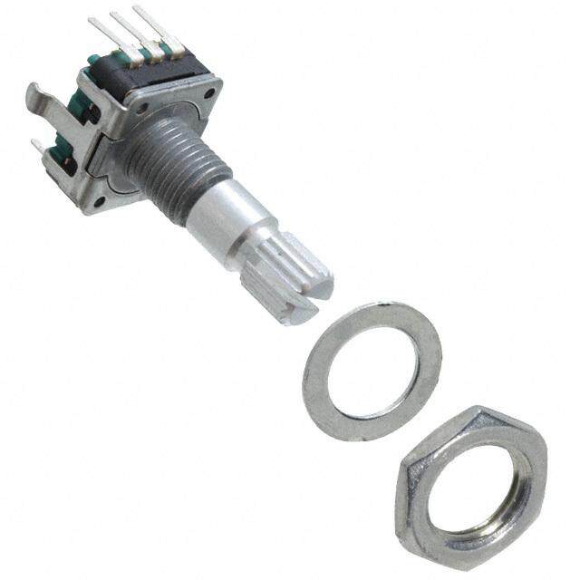
| 描述 | IC ENCODER ROTARY 8-BIT 16-TSSOP |
| 产品分类 | 磁性传感器 - 霍尔效应,数字开关,线性,罗盘 (IC) |
| 品牌 | ams |
| 数据手册 | http://www.ams.com/eng/content/download/11929/212604 |
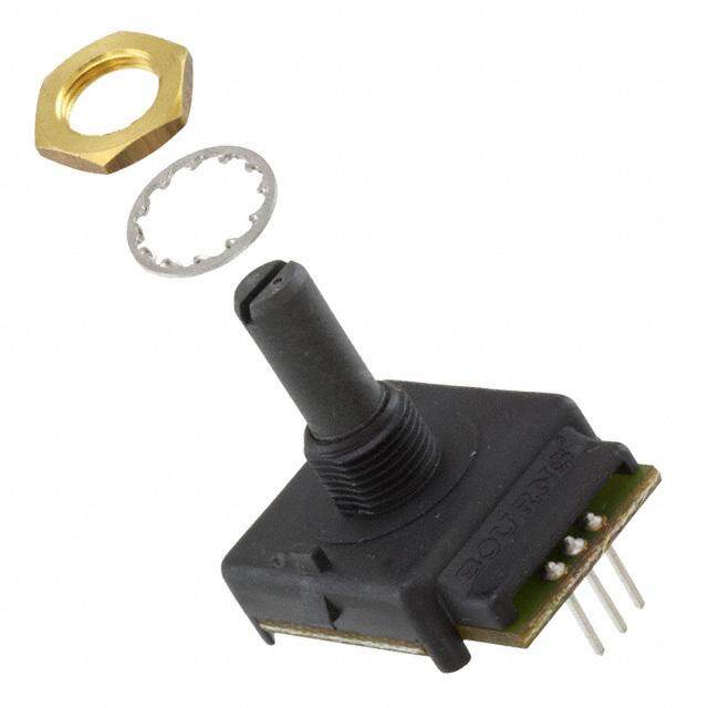
| 产品图片 |
|
| 产品型号 | AS5030-ATST |
| rohs | 无铅 / 符合限制有害物质指令(RoHS)规范要求 |
| 产品系列 | - |
| 产品目录页面 | |
| 供应商器件封装 | 16-TSSOP |
| 其它名称 | AS5030-ATSTDKR |
| 包装 | Digi-Reel® |
| 封装/外壳 | 16-TSSOP(0.173",4.40mm 宽) |
| 工作温度 | -40°C ~ 125°C |
| 应用说明 | http://www.austriamicrosystems.com/eng/content/view/download/11922http://www.austriamicrosystems.com/eng/content/view/download/11921 |
| 感应范围 | 20mT ~ 80mT |
| 标准包装 | 1 |
| 特性 | 可编程 |
| 电压-电源 | 4.5 V ~ 5.5 V |
| 电流-电源 | 14mA |
| 电流-输出(最大值) | 4mA |
| 类型 | 线性,旋转编码器 - 可编程 |
| 输出类型 | 数字,PWM |


- 商务部:美国ITC正式对集成电路等产品启动337调查
- 曝三星4nm工艺存在良率问题 高通将骁龙8 Gen1或转产台积电
- 太阳诱电将投资9.5亿元在常州建新厂生产MLCC 预计2023年完工
- 英特尔发布欧洲新工厂建设计划 深化IDM 2.0 战略
- 台积电先进制程称霸业界 有大客户加持明年业绩稳了
- 达到5530亿美元!SIA预计今年全球半导体销售额将创下新高
- 英特尔拟将自动驾驶子公司Mobileye上市 估值或超500亿美元
- 三星加码芯片和SET,合并消费电子和移动部门,撤换高东真等 CEO
- 三星电子宣布重大人事变动 还合并消费电子和移动部门
- 海关总署:前11个月进口集成电路产品价值2.52万亿元 增长14.8%

PDF Datasheet 数据手册内容提取
AS5030 8-Bit Programmable High Speed Magnetic Rotary Encoder 1 General Description 2 Key Features The AS5030 is a contactless magnetic rotary encoder for accurate 360° contactless angular position encoding angular measurement over a full turn of 360°. Two digital 8-bit absolute outputs: It is a system-on-chip, combining integrated Hall elements, analog front end and digital signal processing in a single device. - Serial interface - Pulse width modulated (PWM) output To measure the angle, only a simple two-pole magnet, rotating over the center of the chip is required. User programmable zero position The absolute angle measurement provides instant indication of the Direct measurement of magnetic field strength allows exact magnet’s angular position with a resolution of 8 bit = 256 positions determination of vertical magnet distance per revolution. This digital data is available as a serial bit stream and Serial read-out of multiple interconnected AS5030 devices as a PWM signal. using daisy chain mode In addition to the angle information, the strength of the magnetic field Wide magnetic field input range: 20 ~ 80mT is also available as a 6-bit code. Wide temperature range: -40°C to +125°C Data transmission can be configured for 1-wire (PWM), 2-wires (CLK, DIO) or 3-wires (CLK, DIO, CS). Small Pb-free package: TSSOP 16 A software programmable (OTP) zero position simplifies assembly 3 Applications as the zero position of the magnet does not need to be mechanically aligned. The AS5030 is suitable for Contactless rotary position sensing, A Power Down Mode together with fast startup- and measurement Rotary switches (human machine interface), AC/DC motor position cycles allows for very low average power consumption and makes control, Robotics and Encoder for battery operated equipment. the AS5030 also suitable for battery operated equipment. Figure 1. AS5030 Block Diagram Sin / Sinn / Cos / Cosn AS5030 PWM PWM Decoder Angle DX Sin Tracking Zero ADC & Absolute DIO Position Cos Angle Serial Hall Array Decoder Interface CS & (SSI) CLK Front-end Mag C2 Amplifier AGC AGC MagRngn Power Management OTP PROG www.ams.com/AS5030 Revision 2.4 1 - 44
AS5030 Datasheet - Contents Contents 1 General Description.................................................................................................................................................................. 1 2 Key Features............................................................................................................................................................................. 1 3 Applications............................................................................................................................................................................... 1 4 Pin Assignments....................................................................................................................................................................... 4 4.1 Pin Descriptions.................................................................................................................................................................................... 4 5 Absolute Maximum Ratings...................................................................................................................................................... 5 6 Electrical Characteristics........................................................................................................................................................... 6 6.1 Operating Conditions............................................................................................................................................................................ 6 6.2 System Parameters.............................................................................................................................................................................. 6 6.3 Magnet Specifications.......................................................................................................................................................................... 7 6.4 Magnetic Field Alarm Limits................................................................................................................................................................. 7 6.5 Hall Element Sensitivity Options........................................................................................................................................................... 7 6.6 Programming Parameters.................................................................................................................................................................... 8 6.7 DC Characteristics of Digital Inputs and Outputs................................................................................................................................. 8 6.8 8-bit PWM Output................................................................................................................................................................................. 9 6.9 Serial 8-bit Output................................................................................................................................................................................. 9 6.10 General Data Transmission Timings................................................................................................................................................ 10 7 Detailed Description................................................................................................................................................................ 11 7.1 Connecting the AS5030...................................................................................................................................................................... 11 7.2 Serial 3-Wire R/W Connection............................................................................................................................................................ 11 7.3 Serial 3-Wire Read-only Connection.................................................................................................................................................. 13 7.4 Serial 2-Wire Connection (R/W Mode)............................................................................................................................................... 14 7.5 Serial 2-Wire Continuous Readout..................................................................................................................................................... 15 7.6 Serial 2-Wire Differential SSI Connection........................................................................................................................................... 15 7.7 1-Wire PWM Connection................................................................................................................................................................ 16 7.8 Analog Output..................................................................................................................................................................................... 18 7.9 Analog Sin/Cos Outputs with External Interpolator............................................................................................................................ 19 7.10 3-Wire Daisy Chain Mode................................................................................................................................................................. 20 7.11 2-Wire Daisy Chain Mode................................................................................................................................................................. 21 8 Application Information........................................................................................................................................................... 22 8.1 AS5030 Programming........................................................................................................................................................................ 23 8.1.1 OTP Programming Options....................................................................................................................................................... 23 8.1.2 Reduced Power Mode Programming Options........................................................................................................................... 23 8.2 AS5030 Read / Write Commands...................................................................................................................................................... 23 8.2.1 16-bit Read Command............................................................................................................................................................... 23 8.2.2 16-bit Write Command............................................................................................................................................................... 24 8.2.3 18-bit OTP Read Commands ................................................................................................................................................... 24 8.2.4 18-bit OTP Write Commands .................................................................................................................................................... 25 8.3 OTP Programming Connection.......................................................................................................................................................... 26 8.3.1 Programming in Daisy Chain Mode........................................................................................................................................... 26 8.4 Programming Verification................................................................................................................................................................... 27 www.ams.com/AS5030 Revision 2.4 2 - 44
AS5030 Datasheet - Contents 8.5 AS5030 Status Indicators................................................................................................................................................................... 27 8.5.1 C2 Status Bit.............................................................................................................................................................................. 27 8.5.2 Lock Status Bit........................................................................................................................................................................... 27 8.5.3 Magnetic Field Strength Indicators............................................................................................................................................ 28 8.5.4 “Push-button” Feature................................................................................................................................................................ 28 8.6 High Speed Operation........................................................................................................................................................................ 29 8.6.1 Propagation Delay..................................................................................................................................................................... 29 8.6.2 Total Propagation Delay of the AS5030 ................................................................................................................................... 30 8.7 Reduced Power Modes...................................................................................................................................................................... 30 8.7.1 Low Power Mode and Ultra-low Power Mode............................................................................................................................ 31 8.7.2 Power Cycling Mode.................................................................................................................................................................. 33 8.8 Accuracy of the Encoder System....................................................................................................................................................... 34 8.8.1 Quantization Error...................................................................................................................................................................... 34 8.8.2 Vertical Distance of the Magnet................................................................................................................................................. 35 8.9 Choosing the Proper Magnet.............................................................................................................................................................. 36 8.9.1 Magnet Placement..................................................................................................................................................................... 37 8.9.2 Lateral Displacement of the Magnet.......................................................................................................................................... 38 8.9.3 Magnet Size............................................................................................................................................................................... 39 8.10 Physical Placement of the Magnet................................................................................................................................................... 40 9 Package Drawings and Markings........................................................................................................................................... 41 9.1 Recommended PCB Footprint............................................................................................................................................................ 42 10 Ordering Information............................................................................................................................................................. 43 www.ams.com/AS5030 Revision 2.4 3 - 44
AS5030 Datasheet - Pin Assignments 4 Pin Assignments Figure 2. Pin Assignments (Top View) MagRngn 1 16 PWM PROG 2 15 C2 0 VSS 3 3 14 C1 test3 4 50 13 VDD test2 5 S 12 DIO A test1 6 11 CS test0 7 10 CLK TC 8 9 DX 4.1 Pin Descriptions Table 1. Pin Descriptions Pin Number Pin Name Pin Type Description Push-Pull output. Is ‘HIGH’ when the magnetic field strength is too 1 MagRngn Digital output / tri-state weak, e.g. due to missing magnet Programming voltage input. Must be left open in normal operation. 2 PROG Supply pin Maximum load = 20pF (except during programming) 3 VSS Supply ground This pin is used for factory testing. For normal operation it must be left 4 T3_SINn - unconnected. Inverse SIN (Sinn) output in SIN/COS output mode This pin is used for factory testing. For normal operation it must be left 5 T2_SIN - unconnected. SIN output in SIN/COS mode This pin is used for factory testing. For normal operation it must be left 6 T1_COSn - unconnected. Inverse COS (Cosn) output in SIN/COS mode This pin is used for factory testing. For normal operation it must be left 7 T0_COS - unconnected. COS output in SIN/COS mode 8 TC - Test pin. Connect to VSS or leave unconnected 9 DX Digital output Digital output for 2-wire operation and Daisy Chain mode 10 CLK Clock Input of Synchronous Serial Interface; Schmitt-Trigger input Digital input / Schmitt-Trigger Chip Select for serial data transmission, active high; Schmitt-Trigger 11 CS input, external pull-down resistor (~50kΩ) required in read-only mode 12 DIO Bi-directional digital pin Data output / command input for digital serial interface 13 VDD Supply pin Positive supply voltage, 4.5V to 5.5V Configuration input: Connect to VSS for normal operation, 14 C1 connect to VDD to enable SIN-COS outputs. This pin is scanned at Digital input power-on-reset and at wake-up from one of the Ultra-low Power Modes (standard CMOS; no pull-up or pull-down) Configuration input: Connect to VSS for 3-wire operation, 15 C2 connect to VDD for 2-wire operation. This pin is scanned at power-on- reset and at wake-up from one of the Ultra-low Power Modes Pulse Width Modulation output, 2µs pulse width per step 16 PWM Digital output (2µs ~ 512µs) www.ams.com/AS5030 Revision 2.4 4 - 44
AS5030 Datasheet - Absolute Maximum Ratings 5 Absolute Maximum Ratings Stresses beyond those listed in Table 2 may cause permanent damage to the device. These are stress ratings only, and functional operation of the device at these or any other conditions beyond those indicated in Electrical Characteristics on page 6 is not implied. Exposure to absolute maximum rating conditions for extended periods may affect device reliability. Table 2. Absolute Maximum Ratings Symbol Parameter Min Max Units Comments Electrical Parameters VDD Supply voltage -0.3 7 V Except during OTP programming VIN Input pin voltage VSS - 0.5 VDD + 0.5 V Iscr Input current (latch-up immunity) -100 100 mA Norm: Jedec 78 Electrostatic Discharge ESD Electrostatic Discharge ±2 kV Norm: MIL 883 E method 3015 137 °C/W Still Air / Single Layer PCB ΘJA Package thermal resistance 89 °C/W Still Air / Multilayer PCB Temperature Ranges and Storage Conditions Tstrg Storage temperature -55 +150 °C Min -67ºF; Max +257ºF The reflow peak soldering temperature (body temperature) specified is in accordance with IPC/JEDEC J-STD-020 “Moisture/Reflow Sensitivity Classification TBODY Body temperature 260 °C for Non-Hermetic Solid State Surface Mount Devices”. The lead finish for Pb-free leaded packages is matte tin (100% Sn). Humidity non-condensing 5 85 % MSL Moisture Sensitive Level 3 Represents a maximum floor time of 168h www.ams.com/AS5030 Revision 2.4 5 - 44
AS5030 Datasheet - Electrical Characteristics 6 Electrical Characteristics TAMB = -40°C to +125°C, VDD5V = 4.5V ~ 5.5V, all voltages referenced to VSS, unless otherwise noted. 6.1 Operating Conditions Symbol Parameter Conditions Min Typ Max Units VDD Positive supply voltage 4.5 5.5 V No load on outputs. 14 18 Minimum AGC (strong magnetic field) IDD Operating current mA No load on outputs. 18 22 Maximum AGC (weak or no magnetic field) Low Power Mode 1400 2000 Ioff Power-down current µA Ultra-low Power Mode 30 120 TAMB Ambient temperature -40°F ~ +257°F -40 125 °C 6.2 System Parameters Symbol Parameter Conditions Min Typ Max Units 8 bit N Resolution 1.406 ° Startup from zero; AGC not regulated 1000 Startup from zero until regulated AGC 3300 Startup from Power Down Mode 500 TPwrUp Power up time μs Startup from Low Power Mode Setting 1: no hysteresis, no reset 46 Setting 2: hysteresis and reset 1500 Analog signal path; tda Propagation delay over full temperature range 15 17 µs step rate of tracking ADC; tdd Tracking rate 1 step = 1.406° 0.85 1.15 1.45 µs Total signal processing delay, tdelay Signal processing delay analog + digital (tda + tdd) 16.15 18.45 µs T Analog filter time constant Internal low-pass filter 4.1 6.6 12.5 µs centered magnet -2 2 INLcm Accuracy within horizontal displacement radius ° -3 3 (see Magnet Specifications on page 7) TN Transition noise rms (1 sigma) 0.235 ° PORr VDD rising 3.5 4.5 V PORf Power-on-reset levels VDD falling 3.0 4.5 V Hyst Hysteresis | PORr - PORf | 500 mV www.ams.com/AS5030 Revision 2.4 6 - 44
AS5030 Datasheet - Electrical Characteristics 6.3 Magnet Specifications Recommended magnet: NdFeB 35H BR = 12.000 Gauss, Ø6mm x 2.5mm Symbol Parameter Conditions Min Typ Max Units MD Magnet diameter Diametrically magnetized 6 mm MT Magnet thickness 2.5 mm Bi Magnetic input range At chip surface, on a radius of 1mm 20 80 mT vi Magnet rotation speed To maintain locked state 30.000 rpm TAMB=25°C, AGC @ lower limit, Bmax Magnetic field high detection 1 sigma = 2.5mT 52 mT TAMB=25°C, AGC @ upper limit, Bmin Magnetic field low detection 1 sigma = 1.5mT 23 Hall array radius Over x/y chip center 1 mm Recommended distance; operation outside Vertical distance of magnet this range is possible, accuracy may be 0.5 1 1.8 mm reduced From diagonal package center 0.25 Horizontal magnet displacement radius mm From diagonal IC center 0.5 NdFeB Material -0.12 Recommended magnet material and tkM temperature drift %/K SmCo Material -0.035 6.4 Magnetic Field Alarm Limits Symbol Parameter Conditions Min Typ Max Units AGCFF Magnetic field too low alarm limit untrimmAeGdC, 2 =5 °FCF,H 1sigma 20.3 23.6 mT AGC0 Magnetic field too high alarm limit untrimmAeGd,C 2 5=° 0CH, 1sigma 44.5 52.2 mT (see Hall Element Sensitivity Options on Magnetic field alarm limit trim range 100 121 % page 7) Sensitivity increases with temperature which Temperature coefficient of alarm ranges partly compensates the temperature 0.052 %/K coefficient of the magnet 6.5 Hall Element Sensitivity Options Symbol Parameter Conditions Min Typ Max Units sens = 00 (default); low sensitivity (see 18-bit OTP Write Commands on page 100 25) sens Hall element sensitivity setting sens = 01 106 % sens = 10 113 sens = 11 (high sensitivity) 121 www.ams.com/AS5030 Revision 2.4 7 - 44
AS5030 Datasheet - Electrical Characteristics 6.6 Programming Parameters Symbol Parameter Conditions Min Typ Max Units VPROG Programming voltage Static voltage at pin PROG 8.0 8.5 V IPROG Programming current 100 mA TambPROG Programming ambient temperature During programming 0 85 °C tPROG Programming time Timing is internally generated 2 4 µs VR,prog 0.5 Analog readback voltage During Analog Readback mode at pin PROG V VR,unprog 2.2 3.5 6.7 DC Characteristics of Digital Inputs and Outputs CMOS Inputs: CLK, CS, DIO, C1, C2 Symbol Parameter Conditions Min Typ Max Units VIH High level input voltage 0.7*VDD V VIL Low level input voltage 0.3*VDD V ILEAK Input leakage current 1 µA CMOS Outputs: DIO, MagRngn, PWM, DX Symbol Parameter Conditions Min Typ Max Units VOH High level output voltage Source current <4mA VDD-0.5 V VOH Low level output voltage Sink current <4mA 0.4 V CL Capacitive load 35 pF CMOS Tristate Output: DIO Symbol Parameter Conditions Min Typ Max Units IOZ Tristate leakage current CS = low 1 µA www.ams.com/AS5030 Revision 2.4 8 - 44
AS5030 Datasheet - Electrical Characteristics 6.8 8-bit PWM Output Symbol Parameter Conditions Min Typ Max Units 8 bit NPWM PWM resolution 2 µs/step PWMIN PWM pulse width Angle = 0° (00H) 1.66 2.26 2.85 µs PWMAX PWM pulse width Angle = 358.6° (FFH) 427 578 731 µs PWP PWM period Over full temperature range1 428 581 734 µs fPWM PWM frequency 1 / PWM period 1.72 kHz Hyst Digital hysteresis2 At change of rotation direction 1 bit 1. The tolerance of the absolute PWM pulse width and frequency can be eliminated by using the duty cycle tON/(tON+tOFF) for angle measurement(see 1-Wire PWM Connection on page 16). 2. Hysteresis may be temporarily disabled by software(see 16-bit Write Command on page 24). 6.9 Serial 8-bit Output 3-wire Interface. Symbol Parameter Conditions Min Typ Max Units fCLK 6 MHz Clock frequency Normal operation tCLK 166.6 ns fclk,P Clock frequency During OTP programming 250 500 kHz 2-wire Interface. Symbol Parameter Conditions Min Typ Max Units fCLK 0.1 6 MHz Clock frequency Normal operation tCLK 166.6 10,000 ns fclk,P Clock frequency During OTP programming 250 500 kHz Rising edge of CLK to internally generated tTO Synchronization timeout chip select on pin DX 16.6 27 34.3 ms Hyst Digital hysteresis1 At change of rotation direction 1 bit 1. Hysteresis may be temporarily disabled by software. www.ams.com/AS5030 Revision 2.4 9 - 44
AS5030 Datasheet - Electrical Characteristics 6.10 General Data Transmission Timings Symbol Parameter Conditions Min Typ Max Units CLK/2 CLK/2 t0 Rising CLK to CS ns +0 +50 t1 Chip select to positive edge of CLK 50 ns t2 Chip select to drive bus externally 0 ns Setup time command bit data valid to t3 50 ns positive edge of CLK Hold time command bit data valid after t4 15 ns positive edge of CLK Float time positive edge of CLK for last t5 CLK/2 +0 ns command bit to bus float Bus driving time positive edge of CLK for CLK/2 t6 ns last command bit to bus drive +0 Setup time data bit data valid to positive CLK/2 CLK/2 t7 ns edge of CLK +0 +30 Hold time data bit data valid after positive CLK/2 t8 ns edge of CLK +0 Hold time chip select positive edge CLK to CLK/2 t9 ns negative edge of chip select +50 Bus floating time negative edge of chip t10 50 ns select to float bus Hold time data bit @ write access t11 50 ns data valid to positive edge of CLK Hold time data bit @ write access t12 15 ns data valid after positive edge of CLK Bus floating time negative edge of chip t13 50 ns select to float bus Timeout period in 2-wire mode tTO (from rising edge of CLK) 20 24 µs See Figure5 for the corresponding timing diagram. www.ams.com/AS5030 Revision 2.4 10 - 44
AS5030 Datasheet - Detailed Description 7 Detailed Description The benefits of AS5030 are as follows: Complete system-on-chip, no calibration required Flexible system solution provides absolute serial and PWM output Ideal for applications in harsh environments due to magnetic sensing principle High reliability due to non-contact sensing Robust system, tolerant to horizontal misalignment, airgap variations, temperature variations and external magnetic fields Figure 3. Typical Arrangement of AS5030 and Magnet 7.1 Connecting the AS5030 The following examples show various ways to connect the AS5030 to an external controller: 7.2 Serial 3-Wire R/W Connection In this mode, the AS5030 is connected to the external controller via three signals: Chip Select (CS), Clock (CLK) inputs and bi-directional DIO (Data In/Out) output. The controller sends commands over the DIO pin at the beginning of each data transmission sequence, such as reading the angle or putting the AS5030 in and out of the reduced power modes. A pull-down resistor is not required. C1 and C2 are hardware configuration inputs. C1 must always be connected to VSS, C2 selects 3-wire mode (C2 = low) or 2-wire mode (C2 = high) www.ams.com/AS5030 Revision 2.4 11 - 44
AS5030 Datasheet - Detailed Description Figure 4. SSI Read/Write Serial Data Transmission +5V VDD 13 VDD VDD 11 Output CS 10 Micro Output CLK AS5030 100n Controller 12 I/O DIO VSS C1 C2 VSS 14 15 3 VSS Figure 5. Timing Diagram in 3-wire SSI R/W Mode command phase data phase t CLK CLK 1 2 3 4 5 6 7 20 21 t1 t9 CS t5 DIO CMD4 CMD3 CMD0 DIO read t7 t8 t3 t6 t10 t4 DIO D15 D14 D1 D0 DIO write Table 3. Serial Bit Sequence (16-bit read/write) Write Command Read / Write Data C4 C3 C2 C1 C0 D15 D14 D13 D12 D11 D10 D9 D8 D7 D6 D5 D4 D3 D2 D1 D0 www.ams.com/AS5030 Revision 2.4 12 - 44
AS5030 Datasheet - Detailed Description 7.3 Serial 3-Wire Read-only Connection If the AS5030 is only used to provide the angular data (no power down or OTP access) this simplified connection is possible. The Chip Select (CS) and Clock (CLK) connection is the same as in the R/W mode, but only a digital input pin (not an I/O pin) is required for the DIO connection. As the first 5 bits of the data transmission are command bits sent to the AS5030, both the microcontroller and the AS5030 are configured as digital inputs during this phase. Therefore, a pull-down resistor must be added to make sure that the AS5030 reads “00000” as the first 5 bits which sets the Read_Angle command. All further application examples are shown in R/W mode, however read-only mode is also possible, unless otherwise noted. Figure 6. SSI Read-only Serial Data Transmission +5 V VDD 13 VDD VDD 11 Output CS 10 Micro Output CLK AS5030 Controller 100n 12 Input DIO 10k... VSS C1 C2 VSS 100k 14 15 3 VSS Figure 7. Timing Diagram in 2-wire and 3-wire SSI Mode command phase data phase CLK 1 2 3 4 5 6 7 8 20 21 t1 t9 CS DIO DIO read t10 DIO D15 D14 D13 D12 D1 D0 DIO write Table 4. Serial Bit Sequence (16-bit read/write) Read D20 D19 D18 D17 D16 D15 D14 D13 D12 D11 D10 D9 D8 D7 D6 D5 D4 D3 D2 D1 D0 AGC Angle 0 0 0 0 0 C2 lock D5 D4 D3 D2 D1 D0 D7 D6 D5 D4 D3 D2 D1 D0 www.ams.com/AS5030 Revision 2.4 13 - 44
AS5030 Datasheet - Detailed Description 7.4 Serial 2-Wire Connection (R/W Mode) By connecting the configuration input C2 to VDD, the AS5030 is configured to 2-wire data transmission mode. Only Clock (CLK) and Data (DIO) signals are required. A Chip Select (CS) signal is automatically generated by the DX output, when a time-out of CLK occurs (typ. 20µs). Note: Read-only mode is also possible in this configuration. Figure 8. SSI R/W Mode 2-wire Data Transmission +5 V VDD 15 13 VDD 9 C2 VDD DX 11 CS 10 Micro Output CLK AS5030 100n Controller 12 I/O DIO VSS C1 VSS 14 3 VSS Figure 9. Timing Diagram in 2-wire SSI Mode wait cycle command phase data phase (>500ns) CLK 1 2 3 4 5 6 7 8 22 t1 t0 DX CS t5 DIO read CMD4 CMD3 CMD2 CMD1 CMD0 t6 DIO write D15 D14 D0 www.ams.com/AS5030 Revision 2.4 14 - 44
AS5030 Datasheet - Detailed Description 7.5 Serial 2-Wire Continuous Readout nd The termination of each readout sequence by a timeout of CLK after the 22 clock pulse as described in Serial 2-Wire Connection (R/W Mode) is the safest method to ensure synchronization, as each timeout of CLK resets the serial interface. However, it is not mandatory to apply a timeout of CLK and consequently synchronization after each reading. It is also possible to read several nd rd consecutive angle values without synchronization by simply continuing the CLK pulses without timeout after the 22 clock. The 23 clock is st equal to the 1 clock of the next measurement, etc. This is the fastest way to read multiple angle values, as there is no timeout period between the readings. It is still possible to synchronize the th serial data transmission by a timeout of CLK after a given number of readouts (e.g. synchronize after every 5 reading, etc.) Figure 10. Timing Diagram in 2-wire SSI Continuous Readout command phase data phase command phase CLK 1 2 3 4 5 6 7 8 22 23 24 25 t1 t0 DX CS t5 DIO read CMD4 CMD3 CMD2 CMD1 CMD0 CMD4 CMD3 CMD2 t6 DIO write D15 D14 D0 1st reading 2nd reading 7.6 Serial 2-Wire Differential SSI Connection With the addition of a RS-422 / RS-485 transceiver, a fully differential data transmission, according to the 21-bit SSI interface standard is possible. To be compatible with this standard, the CLK signal must be inverted. This is done by reversing the Data+ and Data- lines of the transceivers. Note: This type of transmission is read-only. Figure 11. 2-wire SSI Read-only Mode +5 V VDD 15 13 VDD 9 C2 VDD DX 11 CS D+ D- CLK 10 Micro Output CLK Controller D- D+ AS5030 100n MAX 3081 or similar D+ D+ DI 12 Input DIO VSS D- D- C1 VSS 14 3 VSS www.ams.com/AS5030 Revision 2.4 15 - 44
AS5030 Datasheet - Detailed Description Figure 12. Timing Diagram in 2-wire Read only Mode (differential transmission) CLK 1 2 3 4 5 6 7 8 20 21 timeout t TO DI D15 D14 D1 D0 Table 5. SSI Read-only Serial Bit Sequence (21bit read) Read D20 D19 D18 D17 D16 D15 D14 D13 D12 D11 D10 D9 D8 D7 D6 D5 D4 D3 D2 D1 D0 AGC Angle 0 0 0 0 0 C2 lock D5 D4 D3 D2 D1 D0 D7 D6 D5 D4 D3 D2 D1 D0 7.7 1-Wire PWM Connection This configuration uses the least number of wires: only one line (PWM) is used for data, leaving the total number of connection to three, including the supply lines. This type of configuration is especially useful for remote sensors. Ultra-low Power Mode is not possible in this configuration, as there is no bi-directional data transmission. If the AS5030 angular data is invalid, the PWM output will remain at low state. Pins that are not shown may be left open. Note that the PWM output is invalid when the AGC is disabled. Figure 13. Data Transmission with Pulse Width Modulated (PWM) Output +5 V VDD 11 13 VDD CS VDD Micro AS5030 Controller 100n 16 Input PWM VSS C1 C2 VSS 14 15 3 VSS www.ams.com/AS5030 Revision 2.4 16 - 44
AS5030 Datasheet - Detailed Description The minimum PWM pulse width tON (PWM = high) is 1 LSB @ 0° (Angle reading = 00H). 1LSB = nom. 2.26µs. The PWM pulse width increases with 1LSB per step. At the maximum angle 358.6° (Angle reading = FFH), the pulse width tON (PWM = high) is 256 LSB and the pause width tOFF (PWM = low) is 1 LSB. This leads to a total period (tON + tOFF) of 257LSB. PWM out 2.26µs 291.54µs 578.56µs ton 5V 0V 578.56µs 287.02µs 2.26µs toff Position 0 128 255 Table 6. SSI Read-only Serial Bit Sequence (21-bit read) Position Angle High t_high Low t_low Duty-Cycle 0 0° 1 2.26µs 256 578.56µs 0.39% 127 178.59 128 287.02µs 129 291.54µs 49.4% 128 180° 129 291.54µs 128 287.02µs 50.2% 255 358.59° 256 578.56µs 1 2.26µs 99.6% This means that the PWM pulse width is (position + 1) LSB, where position is 0….255. The tolerance of the absolute pulse width and -frequency can be eliminated by calculating the angle with the duty cycle rather than with the absolute pulse width: (EQ 1) [ ] t angle8−bit =257 ON −1 t +t ON OFF results in an 8-bit value from 00H to FFH, (EQ 2) [ ] 360 t angle° = 256257t +ONt −1 ON OFF results in a degree value from 0° ~ 358.6° Note: The absolute frequency tolerance is eliminated by dividing tON by (tON+TOFF), as the change of the absolute timing effects both TON and TOFF in the same way. www.ams.com/AS5030 Revision 2.4 17 - 44
AS5030 Datasheet - Detailed Description 7.8 Analog Output This configuration is similar to the PWM connection (only three lines including supply are required). With the addition of a low-pass filter at the PWM output, this configuration produces an analog voltage that is proportional to the angle. This filter can be either passive (as shown) or active. The lower the bandwidth of the filter, the less ripple of the analog output can be achieved. If the AS5030 angular data is invalid, the PWM output will remain at low state and thus the analog output will be 0V. Pins that are not shown may be left open. Note: The PWM output is invalid when the AGC is disabled. Figure 14. Data Transmission with Pulse Width Modulated (PWM) Output +5 V VDD 11 13 CS VDD AS5030 100n >=4k7 >=4k7 16 Analog PWM out C1 C2 VSS >=1µF >=1µF 14 15 3 VSS Figure 15. Relation of PWM/Analog Output With Angle 5V Analog out 0V PWMout Angle 0° 180° 360° www.ams.com/AS5030 Revision 2.4 18 - 44
AS5030 Datasheet - Detailed Description 7.9 Analog Sin/Cos Outputs with External Interpolator By connecting C1 to VDD, the AS5030 provides analog Sine and Cosine outputs (Sin, Cos) of the Hall array front-end for test purposes. These outputs allow the user to perform the angle calculation by an external ADC + µC, e.g. to compute the angle with a high resolution. In addition, the inverted Sine and Cosine signals (Sinn, Cosn; see dotted lines) are available for differential signal transmission. The input resistance of the receiving amplifier or ADC should be greater than 100kΩ. The signal lines should be kept as short as possible, longer lines should be shielded in order to achieve best noise performance. The SIN / COS / SINn / COSn signals are amplitude controlled to ~1.3Vp (differential) by the internal AGC controller. The DC bias voltage is 2.25V. If the SIN(n)- and COS(n)- outputs cannot be sampled simultaneously, it is recommended to disable the automatic gain control as the signal amplitudes may be changing between two readings of the external ADC. This may lead to less accurate results. Figure 16. Sine and Cosine Outputs for External Angle Calculation +5 V VDD 14 13 VDD C1 VDD 5 Sin D A 4 Sinn Micro AS5030 Controller 7 100n Cos D A 6 Cosn VSS C2 VSS 15 3 VSS www.ams.com/AS5030 Revision 2.4 19 - 44
AS5030 Datasheet - Detailed Description 7.10 3-Wire Daisy Chain Mode The Daisy Chain mode allows connection of more than one AS5030 to the same controller interface. Independent of the number of connected devices, the interface to the controller remains the same with only three signals: CSn, CLK and DO. In Daisy Chain mode, the data from the second and subsequent devices is appended to the data of the first device. The 100nF buffer cap at the supply (shown only for the last device) is recommended for all devices. The total number of serial bits is: n*21, where n is the number of connected devices: e.g. for 2 devices, the serial bit stream is 42bits. For three devices it is 63 bits. Figure 17. Connection of Devices in 3-wire Daisy Chain Mode +5V VDD 13 13 13 VDD VDD VDD VDD Micro AS5030 AS5030 AS5030 Controller #1 #2 (last device) 11 11 11 Output CS DX CS DX CS DX 100n 10 10 10 Output CLK CLK CLK 12 12 12 I/O DIO DIO DIO VSS C1 C2 VSS C1 C2 VSS C1 C2 VSS 14 15 3 14 15 3 14 15 3 VSS Figure 18. Timing Diagram in 3-wire Daisy Chain Mode CLK 1 2 3 4 5 6 7 8 20 21 22 23 24 25 26 27 28 29 41 42 43 44 CS DIO CMD4 CMD3 CMD2 CMD1 CMD0 D15 D14 D13 D0 CMD4 CMD3 CMD2 CMD1 CMD0 D15 D14 D13 D0 CMD4 CMD3 CMD2 AS5030 #1 AS5030 #2 AS5030 #3 www.ams.com/AS5030 Revision 2.4 20 - 44
AS5030 Datasheet - Detailed Description 7.11 2-Wire Daisy Chain Mode The AS5030 can also be connected in 2-wire Daisy Chain mode, requiring only two signals (Clock and Data) for any given number of daisy- chained devices. Note that the connection of all devices except the last device is the same as for the 3-wire connection (see Figure 17). The last device must have pin C2 (#15) set to ‘high’ and feeds the DX signal to CS of the first device. Again, each device should be buffered with a 100nF cap (shown only for the last device). The total number of serial bits is: n*21, where n is the number of connected devices. Note that this configuration requires one extra clock (#1) to initiate the generation of the CS signal for the first device. After reading the last device, the communication must be reset back to the first device by introducing a timeout of CLK (no rising edge for >24µs) Figure 19. 2-wire Daisy Chain Mode +5V VDD 13 13 13 15 VDD VDD VDD VDD C2 Micro AS5030 AS5030 AS5030 Controller 11 #1 #2 (last device) CS 11 11 DX CS DX CS DX 100n 10 10 10 Output CLK CLK CLK 12 12 12 I/O DIO DIO DIO VSS C1 C2 VSS C1 C2 VSS C1 VSS 14 15 3 14 15 3 14 3 VSS Figure 20. Timing Diagram in 2-wire Daisy Chain Mode CLK 1 2 3 4 5 6 7 8 21 22 23 24 25 26 27 28 29 42 43 44 45 CS (#1) CS (#2) CS (#3) DIO CMD4 CMD3 CMD2 CMD1 CMD0 D15 D14 D0 CMD4 CMD3 CMD2 CMD1 CMD0 D15 D14 D0 CMD4 CMD3 CMD2 AS5030 #1 AS5030 #2 AS5030 #3 www.ams.com/AS5030 Revision 2.4 21 - 44
AS5030 Datasheet - Application Information 8 Application Information AS5030 Parameter and Features List. Parameter Description Supply voltage 5V ± 10% Low Power Mode, non-operational: typ. 1.4mA Supply current Ultra-low Power Mode, non-operational: typ. 30µA Normal operating mode: typ. 14mA. 21-bit Synchronous Serial Interface (SSI): 5 command bits, 2 data valid bits, 6 data bits for magnetic field strength, 8 data bits for angle. Absolute output; Serial Interface Configurable for 2-wire (Clock, Data) or 3-wire (Chip Select, Clock, Data) operation Daisy Chain mode for reading multiple encoders through a 2- or 3-wire interface. Zero Position Programming (OTP) SSI clock rate ≤ 6 MHz data clock rate, 250 ~ 500kHz during programming 2-wire readout mode DIO and CLK signals. 0.1 ~ 6MHz clock rate. Synchronization through time-out of CLK signal. Activated and deactivated by software commands. Power down modes Low Power Mode: power down current = 1.4mA typ.; power up time <150µs Ultra-low Power Mode: power down current = 30µA typ.; power up time <500µs Digital input cells CLK, CS = Schmitt trigger inputs SIN-COS mode Sine, inverse Sine, Cosine and inverse Cosine outputs. 360° per period. Maximum speed 30.000 rpm with locked ADC Resolution = 8-bit (1.406°) Resolution and accuracy Accuracy ≤ ± 2° with centered magnet Transition noise 0.24°rms (1 sigma) PWM output 2.26µs / Step, PWM will be permanently low when angular data is not valid (e.g. during startup). Digital output current 4mA @ VDD = 5V (PWM, DIO, DX, MagRngn outputs) Through serial interface with static programming voltage on pin #2 (PROG) 16-bit OTP programming register. OTP user programming options: OTP programming mode Angular zero position: 8 bit Hall element sensitivity: 2 bit Trimmable in four steps with OTP programming (sensitivity) Magnetic field range maximum/minimum ratio ~ 2.5:1. Field range window = 20 ~ 80mT (e.g. maximum sensitivity range = 20 ~ 48mT, minimum sensitivity range = 32 ~ 80mT By hardware: MagRngn pin indicates locked condition of ADC Non-valid-range indication By software: LOCK1&2 status bits indicate locked condition of ADC Start-up time after shutdown < 2ms Start-up timings Start-up time after power-down from Ultra-low Power Mode: < 500µs Start-up time after power-down from Low Power Mode: < 150µs ESD protection ± 2kV Operating temperature -40°C ~ +125°C www.ams.com/AS5030 Revision 2.4 22 - 44
AS5030 Datasheet - Application Information 8.1 AS5030 Programming The AS5030 has an integrated 18-Bit OTP ROM for configuration purposes. 8.1.1 OTP Programming Options The OTP programming options can be set permanently by programming or temporarily by overwriting. Both methods are carried out over the serial interface, but with different commands (WRITE OTP, PROG OTP). Note: During the 18bit OTP programming, each bit needs 4 clock pulses to be validated. Zero Position Programming This programming option allows the user to program any rotation angle of the magnet as the new zero position. This useful feature simpli- fies the assembly process as the magnet does not need to be mechanically adjusted to the electrical zero position. It can be assembled in any rotation angle and later matched to the mechanical zero position by zero position programming. The 8-bit user programmable zero position can be applied both temporarily (command WRITE OTP, #1FH) or permanently (command PROG OTP, #19H) Magnetic Field Optimization This programming option allows the user to match the vertical distance of the magnet with the optimum magnetic field range of the AS5030 by setting the sensitivity level. The 2-bit user programmable sensitivity setting can be applied both temporarily (command WRITE OTP, #1FH) or permanently (command PROG OTP, #19H) 8.1.2 Reduced Power Mode Programming Options These temporary programming options are also carried out over the serial interface. Low Power Mode Low Power Mode is a power saving mode with fast start-up. In Low Power Mode, all internal digital registers are frozen and the power con- sumption is reduced to max. 1.5mA. The serial interface remains active. Start-up from this mode to normal operation can be accomplished within 150µs. This mode is recommended for applications, where low power, but fast start-up and short reading cycle intervals are required. Ultra-low Power Mode Ultra-low Power Mode is a power saving mode with even reduced power-down current consumption. In this mode, all chip functions are fro- zen and the power consumption is reduced to max. 50µA. The serial interface remains active. Start-up from this mode to normal operation can be accomplished within 500µs. This mode is recommended for applications, where very low average power consumption is required, e.g. for battery operated equipment. For example, in a cycled operation with 10 readings per second, the average power consumption of the AS5030 can be reduced to only 120µA. 8.2 AS5030 Read / Write Commands Data transmission with the AS5030 is handled over the 2-wire or 3-wire interface. The transmission protocol begins with sending a 5-bit command to the AS5030, followed by reading or writing 16 or 18 bits of data: 8.2.1 16-bit Read Command Command Bin Hex D15 D14 D13 D12 D11 D10 D9 D8 D7 D6 D5 D4 D3 D2 D1 D0 RD 00000 00 C2 lock AGC 5:0 Angle 7:0 ANGLE C2 displays status of hardware pin C2 (pin #15) Lock indicates that the AGC is locked. Data is invalid when this bit is 0 AGC 6-bit AGC register. Indicates the strength of the magnet (e.g. for push-button applications) 000000b indicates a strong magnetic field 111111b indicates a weak magnetic field ideally, the vertical distance of the magnet should be chosen such that the AGC value is in the middle (around 100000b) Angle 8-bit Angle value; represents the rotation angle of the magnet. One step = 360°/256 = 1.4° www.ams.com/AS5030 Revision 2.4 23 - 44
AS5030 Datasheet - Application Information 8.2.2 16-bit Write Command These settings are temporary; they cannot be programmed permanently. The settings will be lost when the power supply is removed. Command Bin Hex D15 D14 D13 D12 D11 D10 D9 D8 D7 D6 D5 D4 D3 D2 D1 D0 EN PROG 10000 10 1 0 0 0 1 1 0 0 1 0 1 0 1 1 1 0 SET PWR ULP/ 10001 11 PSM 0 MODE LPn DIS HYST 10011 13 HYS 0 DIS AGC 10101 15 0 0 0 0 0 rst 0 0 0 AGC 5:0 FA EN PROG command must be sent with a fixed 16-bit code (8CAEH) to enable subsequent OTP access. ULP/LPn selects the Ultra-low Power Mode, when bit PSM is set: 0 = Low Power Mode, 1 = Ultra-low Power Mode PSM enables power saving modes: 0 = normal operation, 1 = reduced power mode selected by bit ULP/LPn HYS disables the hysteresis of the digital serial and PWM outputs: 0 (default) = 1-bit hysteresis, 1 = no hysteresis DIS AGC disables the automatic gain control. The AGC will be frozen to a gain setting written in bits AGC 5:0 (D6:D1), bit FA must be set. rst General Reset: 0 = normal operation, 1 = perform general reset (required after return from reduced power modes) FA Freeze AGC; 0 = normal operation, 1= freeze AGC with the values stored in bits AGC 5:0. The PWM output will be invalid when bit FA is set. 8.2.3 18-bit OTP Read Commands Note: To prohibit unintentional access to the OTP register, OTP PROG/write access is only enabled after the EN PROG command has been sent. OTP access is locked again by sending a RD ANGLE or SET PWR MODE command. EN PROG need not to be sent before a READ OTP. During the 18bit OTP read/write transfer, each bit needs 4 clock pulses to be validated. Command Bin Hex D17 D16 D15 D14 D13 D12 D11 D10 D9 D8 D7 D6 D5 D4 D3 D2 D1 D0 sens zero position READ OTP 01111 0F reserved for factory settings 1:0 7:0 ANALOG sens zero position 01001 09 reserved for factory settings OTP RD 1:0 7:0 READ OTP reads the contents of the OTP register in digital form. The reserved area may contain any value ANALOG OTP RD reads the contents of the OTP register as an analog voltage at pin PROG sens reads the sensitivity setting of the Hall elements: 00 = low sensitivity, 11 = high sensitivity zero position reads the programmed zero position; the actual angle of the magnet which is displayed as 000 www.ams.com/AS5030 Revision 2.4 24 - 44
AS5030 Datasheet - Application Information 8.2.4 18-bit OTP Write Commands During the 18bit OTP read/write transfer, each bit needs 4 clock pulses to be validated. Command Bin Hex D17 D16 D15 D14 D13 D12 D11 D10 D9 D8 D7 D6 D5 D4 D3 D2 D1 D0 WRITE copy factory settings sens zero position 11111 1F OTP obtained from READ OTP command 1:0 7:0 00000000 sens zero position PROG OTP 11001 19 reserved for factory settings, 1:0 7:0 WRITE OTP: non-permanent (“soft write”) modification of the OTP register. To set the reserved factory settings area properly, a preceding READ OTP command must be made to receive the correct setting for bits D17:D10. The WRITE OTP command must then set these bits in exactly the same way. Improper setting of the factory settings by a WRITE OTP command may cause malfunction of the chip. The OTP register, including the factory settings can be restored to default by a power-up cycle. For non-permanent writing, a programming voltage at pin PROG (#2) is not required. EN_PROG must be sent before WRITE_OTP to enable OTP. PROG OTP: permanent modification of the OTP register. An unprogrammed OTP bit contains a ‘0, programmed bits are 1’s. It is possible to program the OTP in several sequences. However, only a 0 can be programmed to 1. Once programmed, an OTP bit cannot be set back to 0. For subsequent programming, bits that are already programmed should be set to 0 to avoid double programming. During permanent programming, the factory settings D17:D10 should always be set to zero to avoid modification of the factory settings. Modifying the factory settings may cause irreversible malfunction of the chip. For permanent programming, a static programming voltage of 8.0-8.5V must be applied at pin PROG (#2). EN_PROG must be sent before PROG_OTP to enable OTP. sens sets the sensitivity setting of the Hall elements: 00: gain factor = 1.65 (low sensitivity) 01: gain factor = 1.75 10: gain factor = 1.86 11: gain factor = 2.00 (high sensitivity) zero position sets the user programmable zero position; the actual angle of the magnet which is displayed as 000 Figure 21. Timing Diagram in OTP 18-bit Read/Write Mode Command phase Data phase extended DCLK t0 t1 t9 CS t2 t5 DIO HI HI CMD2 CMD0 DIO t3 t4 t6 t8 t7 t10 READ D17 D16 D0 t11 t12 t13 DIO D17 D16 D0 WRITE www.ams.com/AS5030 Revision 2.4 25 - 44
AS5030 Datasheet - Application Information 8.3 OTP Programming Connection Programming of the AS5030 OTP memory does not require a dedicated programming hardware. The programming can be simply accomplished over the serial 3-wire interface (see Figure 22) or the optional 2-wire interface (see Figure 8). For permanent programming (command PROG OTP, #19H), a constant DC voltage of 8.0V ~ 8.5V (≥100mA) must be connected to pin #2 (PROG). For temporary OTP write (“soft write”; command WRITE OTP, #1FH), the programming voltage is not required. To secure unintentional programming, any modification of the OTP memory is only enabled after a special password (command #10H) has been sent to the AS5030. Figure 22. OTP Programming Connection +5 V VDD 13 VDD VDD 11 Output CS 10 Output CLK Micro 12 AS5030 Controller I/O DIO 100n 8.0 –8.5V 2 PROG 10µF 100n VSS C1 C2 VSS 14 15 3 VSS 8.3.1 Programming in Daisy Chain Mode Programming in Daisy chain mode is possible for both 3-wire and 2-wire mode (see Figure17 and Figure19). For temporary programming (soft write), no additional connections are required. Programming is executed with the respective programming commands. For permanent programming, the programming voltage must be applied on pin#2 (PROG) of the device to be programmed. It is also possible to apply the programming voltage simultaneously to all devices, as the actual programming is only executed by a software command. A parallel connection of all PROG-pins allows digital programming verification but does not allow analog programming verification. If analog programming verification is required, each PROG pin must be selected individually for verification. www.ams.com/AS5030 Revision 2.4 26 - 44
AS5030 Datasheet - Application Information 8.4 Programming Verification After programming, the programmed OTP bits may be verified in two ways: - By digital verification: this is simply done by sending a READ OTP command (#0FH). The structure of this register is the same as for the OTP PROG or OTP WRITE commands. - By analog verification: By sending an ANALOG OTP READ command (#09H), pin PROG becomes an output, sending an analog voltage with each clock, representing a sequence of the bits in the OTP register. A voltage of <500mV indicates a correctly programmed bit (“1”) while a voltage level between 2.2V and 3.5V indicates a correctly unprogrammed bit (“0”). Any voltage level in between indicates improper programming. Figure 23. Analog OTP Verification +5 V VDD 13 VDD VDD 11 Output CS 10 Output CLK Micro 12 AS5030 Controller I/O DIO 100n 2 PROG VSS V C1 C2 VSS 14 15 3 VSS 8.5 AS5030 Status Indicators Refer to 16-bit Read Command on page 23. 8.5.1 C2 Status Bit This bit represents the hardware connection of the C2 configuration pin (#15) to determine, which hardware configuration is selected for the AS5030 in question. C2 = low: pin C2 is ‘low’, indicating that the AS5030 is in 3-wire mode or a member of a 2-wire daisy chain connection (except the last) C2 = high: pin C2 is ‘high’, indicating that the AS5030 is in 2-wire mode and/or the last member of a 2-wire daisy chain connection 8.5.2 Lock Status Bit The Lock signal indicates the ADC lock status. If Lock = low (ADC unlocked), the angle information is invalid. To determine a valid angular signal at best performance, the following indicators should be set: Lock = 1 AGC > 00H and < 2FH Note: The angle signal may also be valid (Lock = 1), when the AGC is out of range (00H or 2FH), but the accuracy of the AS5030 may be reduced due to the out of range condition of the magnetic field strength. www.ams.com/AS5030 Revision 2.4 27 - 44
AS5030 Datasheet - Application Information 8.5.3 Magnetic Field Strength Indicators The AS5030 is not only able to sense the angle of a rotating magnet, it can also measure the magnetic field strength (and hence the vertical distance) of the magnet. This extra feature can be used for several purposes: - as a safety feature by constantly monitoring the presence and proper vertical distance of the magnet - as a state-of-health indicator, e.g. for a power-up self test - as a push-button feature for rotate-and-push types of manual input devices The magnetic field strength information is available in two forms: Magnetic Field Strength Hardware Indicator: Pin MagRngn (#1) will be ‘high’, when the magnetic field is too weak. The switching limit is determined by the value of the AGC. If the AGC value is <3FH, the MagRngn output will be ‘low’ (green range), If the AGC is at its upper limit (3FH), the MagRngn output will be ‘high’ (red range). Magnetic Field Strength Software Indicator: D13:D7 in the serial data that is obtained by command READ ANGLE contains the 6-bit AGC information. The AGC is an automatic gain control that adjusts the internal signal amplitude obtained from the Hall elements to a constant level. If the magnetic field is weak, e.g. with a large vertical gap between magnet and IC, with a weak magnet or at elevated temperatures of the magnet, the AGC value will be ‘high’. Likewise, the AGC value will be lower when the magnet is closer to the IC, when strong magnets are used and at low temperatures. The best performance of the AS5030 will be achieved when operating within the AGC range. It will still be operational outside the AGC range, but with reduced performance especially with a weak magnetic field due to increased noise. Factors Influencing the AGC Value. In practical use, the AGC value will depend on several factors: The initial strength of the magnet. Aging magnets may show a reducing magnetic field over time which results in an increase of the AGC value. The effect of this phenomenon is relatively small and can easily be compensated by the AGC. The vertical distance of the magnet. Depending on the mechanical setup and assembly tolerances, there will always be some variation of the vertical distance between magnet and IC over the lifetime of the application using the AS5030. Again, vertical distance variations can be compensated by the AGC The temperature and material of the magnet. The recommended magnet for the AS5030 is a diametrically magnetized, 5-6mm diameter NdFeB (Neodymium-Iron-Boron) magnet. Other magnets may also be used as long as they can maintain to operate the AS5030 within the AGC range. Every magnet has a temperature dependence of the magnetic field strength. The temperature coefficient of a magnet depends on the used material. At elevated temperatures, the magnetic field strength of a magnet is reduced, resulting in an increase of the AGC value. At low temperatures, the magnetic field strength is increased, resulting in a decrease of the AGC value. The variation of magnetic field strength over temperature is automatically compensated by the AGC. OTP Sensitivity Adjustment. To obtain best performance and tolerance against temperature or vertical distance fluctuations, the AGC value at normal operating temperature should be in the middle between minimum and maximum, hence it should be around 100000 (20H). To facilitate the “vertical centering” of the magnet+IC assembly, the sensitivity of the AS5030 can be adjusted in the OTP register in 4 steps. A sensitivity adjustment is recommended, when the AGC value at normal operation is close to its lower limit (around 00H). The default sensitivity setting is 00H = low sensitivity. 8.5.4 “Push-button” Feature Using the magnetic field strength software and hardware indicators described above, the AS5030 provides a useful method of detecting both rotation and vertical distance simultaneously. This is especially useful in applications implementing a rotate-and-push type of human interface (e.g. in panel knobs and switches). The MagRngn output is ‘high’, when the magnetic field is below the low limit (weak or no magnet) and low when the magnetic field is above the low limit (in-range or strong magnet). A finer detection of a vertical distance change, for example when only short vertical strokes are made by the push-button, is achieved by memorizing the AGC value in normal operation and triggering on a change from that nominal the AGC value to detect a vertical movement. www.ams.com/AS5030 Revision 2.4 28 - 44
AS5030 Datasheet - Application Information Figure 24. Magnetic Field Strength Indicator +5 V VDD 1k 13 VDD LED1 VDD 1 MagRngn 11 Micro Output CS AS5030 Controller 10 100n Output CLK 12 I/O DIO VSS C1 C2 VSS 14 15 3 VSS 8.6 High Speed Operation The AS5030 is using a fast tracking ADC (TADC) to determine the angle of the magnet. The TADC has a tracking rate of 1.15µs (typ). Once the TADC is synchronized with the angle, it sets the LOCK bit in the status register. In worst case, usually at start-up, the TADC requires a maximum of 127 steps (127 * 1.15µS = 146.05µs) to lock. Once it is locked, it requires only one cycle (1.15µs) to track the moving magnet. The AS5030 can operate in locked mode at rotational speeds up to 30.000 rpm. In Low Power Mode or Ultra-low Power Mode, the position of the TADC is frozen. It will continue from the frozen position once it is powered up again. If the magnet has moved during the power down phase, several cycles will be required before the TADC is locked again. The tracking time to lock in with the new magnet angle can be roughly calculated as: (EQ 3) t =1.15μs∗ NewPos−OldPos LOCK Where: tLOCK = time required to acquire the new angle after power up from one of the reduced power modes [µs] OldPos = Angle position when one of the reduced power modes is activated [°] NewPos = Angle position after resuming from reduced power mode [°] 8.6.1 Propagation Delay The Propagation delay is the time required from reading the magnetic field by the Hall sensors to calculating the angle and making it available on the serial or PWM interface. While the propagation delay is usually negligible on low speeds it is an important parameter at high speeds. The longer the propagation delay, the larger becomes the angle error for a rotating magnet as the magnet is moving while the angle is calculated. The position error increases linearly with speed. The main factors contributing to the propagation delay are: ADC Sampling Rate. For high speed applications, fast ADCs are essential. The ADC sampling rate directly influences the propagation delay. The fast tracking ADC used in the AS5030 with a tracking rate of only 1.15µs (typ.) is a perfect fit for both high speed and high performance. www.ams.com/AS5030 Revision 2.4 29 - 44
AS5030 Datasheet - Application Information Chip Internal Low-pass Filtering. A commonplace practice for systems using analog-to-digital converters is to filter the input signal by an anti-aliasing filter. The filter characteristic must be chosen carefully to balance propagation delay and noise. The low-pass filter in the AS5030 has a cut-off frequency of typ. 23.8kHz and the overall propagation delay in the analog signal path is typ. 15.6µs. Digital Readout Rate. Aside from the chip-internal propagation delay, the time required to read and process the angle data must also be considered. Due to its nature, a PWM signal is not very usable at high speeds, as you get only one reading per PWM period. Increasing the PWM frequency may improve the situation but causes problems for the receiving controller to resolve the PWM steps. The frequency on the AS5030 PWM output is typ. 1.95kHz with a resolution of 2µs/step. A more suitable approach for high speed absolute angle measurement is using the serial interface. With a clock rate of up to 6MHz, a complete set of data (21bits) can be read in >3.5µs 8.6.2 Total Propagation Delay of the AS5030 The total propagation delay of the AS5030 is the delay in the analog signal path and the tracking rate of the ADC: 15.6µs + 1.15µs = 16.75µs. If only the SIN-/COS-outputs are used, the propagation delay is the analog signal path delay only (typ. 15.6µs). Position Error over Speed. The angle error over speed caused by the propagation delay is calculated as: -6 Δφpd = rpm * 6 * 16.75E in degrees (EQ 4) In addition, the anti-aliasing filter causes an angle error calculated as: Δφlpf = ArcTan [ rpm / ( 60*f0 ) ] (EQ 5) Examples of the overall position error caused by speed, including both propagation delay and filter delay: Total Position Error Speed (rpm) (Δφpd + Δφlpf) 100 0.0175° 1000 0.175° 10000 1.75° 8.7 Reduced Power Modes The AS5030 can be operated in 3 reduced power modes. All 3 modes have in common that they switch off or freeze parts of the chip during intervals between measurements. In Low Power Mode or Ultra-low Power Mode, the AS5030 is not operational, but due to the fast start-up, an angle measurement can be accomplished very quickly and the chip can be switched to reduced power immediately after a valid measurement has been taken. Depending on the intervals between measurements, very low average power consumption can be achieved using such a strobed measurement mode. Low Power Mode:reduced current consumption, very fast start-up. Ideal for short sampling intervals (<3ms) Ultra-low Power Mode:further reduced current consumption, but slower start-up than Low Power Mode. Ideal for sampling intervals from 3….200ms Power Cycle mode:zero power consumption (externally switched off) during sampling intervals, but slower start-up than Ultra-low Power Mode. Ideal for sampling intervals 200ms www.ams.com/AS5030 Revision 2.4 30 - 44
AS5030 Datasheet - Application Information 8.7.1 Low Power Mode and Ultra-low Power Mode Figure 25. Low Power Mode and Ultra-low Power Mode Connection R1s: eoep ttieoxntal; +5V VDD VDD IIoonff ton toff VDD on/off C1: optional; CS Micro see text 100n S N CLK Controller DIO AS5030 VSS C1 C2 VSS VSS The AS5030 can be put in Low Power Mode or Ultra-low Power Mode by simple serial commands, using the regular connection for 2-wire or 3- wire serial data transmission (see Figure4 and Figure8). The required serial command is SET PWR MODE (11H): ULP / LPn PSM Mode 0 0 Normal operation 0 1 Low Power Mode 1 0 Normal operation 1 1 Ultra-low Power Mode Note: After returning from Low Power mode or Ultra-low Power mode to normal operation (PSM = 0), if the Hysteresis is enabled (Hys=0), a general reset must be performed: set bit RST and then clear bit RST using command 15H. The two following cases describe the typical loop programmed in the software: Hys = 0. (1 LSB hysteresis) 1. Wait for CPU interrupt or delay for next angle read (typ. <3ms in LP mode, typ>3ms in ULP mode) 2. Wake up (PSM = 0) 3. Set Reset (rst = 1) 4. Clear Reset (rst = 0) 5. Wait 1.5ms (Low Power Mode) 6. Check if Lock = 1 then read angle 7. Enable Low Power Mode or Ultra-low Power Mode (PSM=1) 8. Return to 1 www.ams.com/AS5030 Revision 2.4 31 - 44
AS5030 Datasheet - Application Information Hys = 1. (No hysteresis) 1. Wait for CPU interrupt or delay for next angle read (typ. <3ms in LP mode, typ>3ms in ULP mode) 2. Wake up (PSM = 0) 3. Wait 0.01ms (Low Power Mode) 4. Check if Lock = 1 then read angle 5. Enable Low Power Mode or Ultra-low Power Mode (PSM=1) 6. Return to 1 The difference between Low Power Mode and Ultra-low Power Mode is the current consumption and the wake-up time to switch back to active operation. Current Consumption Wake-up Time to Active Mode (typ.) Operation 1.0 ms (without AGC) Active operation 14 mA 3.8 ms (with locked AGC) Low Power Mode 1.4 mA 0.15 ms Ultra-low Power Mode 30 µA 0.5 ms In both Reduced Power Modes, the AS5030 is inactive. The last state, e.g. the angle, AGC value, etc. is frozen and the chip starts from this frozen state when it resumes active operation. This method provides much faster start-up than a “cold start” from zero. If the AS5030 is cycled between active and reduced current mode, a substantial reduction of the average supply current can be achieved. The minimum dwelling time in active mode is the wake-up time. The actual active time depends on how much the magnet has moved while the AS5030 was in reduced power mode. The angle data is valid, when the status bit LOCK has been set. Once a valid angle has been measured, the AS5030 can be put back to reduced power mode. The average power consumption can be calculated as: (EQ 6) I ∗t +I ∗t I = active on power_down off avg t +t on off sampling interval = ton + toff Where: Iavg average current consumption Iactive: current consumption in active mode Ipower_down:current consumption in reduced power mode ton:time period during which the chip is operated in active mode toff: time period during which the chip is in reduced power mode Example: Ultra-low Power Mode; sampling period = one measurement every 10ms. System constants = Iactive = 14mA, Ipower_down = 30µA, ton(min) = 500µs (startup from Ultra-low Power Mode): (EQ 7) 14mA∗500μs+30μA*9,5ms I = =729μA avg 500μs+9,5ms See Figure27 for an overview table of the average current consumption in the various reduced power modes. Reducing Power Supply Peak Currents. An optional RC-filter (R1/C1) may be added to avoid peak currents in the power supply line when the AS5030 is toggled between active and reduced power mode. R1 must be chosen such that it can maintain a VDD voltage of 4.5V ~ 5.5V under all conditions, especially during long active periods when the charge on C1 has expired. C1 should be chosen such that it can support peak currents during the active operation period. For long active periods, C1 should be large and R1 should be small. www.ams.com/AS5030 Revision 2.4 32 - 44
AS5030 Datasheet - Application Information 8.7.2 Power Cycling Mode The power cycling method shown in Figure26 cycles the AS5030 by switching it on and off, using an external PNP transistor high side switch. This mode provides the least power consumption of all three modes; when the sampling interval is more than 400ms, as the current consumption in off-mode is zero. It also has the longest start-up time of all modes, as the chip must always perform a “cold start“ from zero, which takes about 1.9 ms. The optional filter R1/C1 may again be added to reduce peak currents in the 5V power supply line. Figure 26. Application Example III: Ultra-low Power Encoder R1 +5V VDD I0on ton toff ton toff VDD 10k C1 VDD >1µF on/off CS Micro 100n S N CLK Controller DIO AS5030 VSS C1 C2 VSS VSS Figure26 shows an overview of the average supply currents in the three reduced power modes, depending on the sampling interval. The graphs shows that the Low Power Mode is the best option for sampling intervals <4ms, while the Ultra-low Power Mode is the best option for sampling intervals between 4~400ms. At sampling intervals > 400ms, the power cycling mode is the best method to minimize the average current consumption. The curves are based on the figures given in Low Power Mode and Ultra-low Power Mode on page 31. Figure 27. Average Current Consumption of Reduced Power Modes AS5030 average current consumption 5,0 4,5 4,0 A m n [ 3,5 o mpti 3,0 u s on 2,5 c nt e 2,0 urr Low Power Mode c g. 1,5 v a 1,0 Power Cycling Mode 0,5 Ultra Low Power Mode 0,0 1 10 100 1000 sampling interval [ms] www.ams.com/AS5030 Revision 2.4 33 - 44
AS5030 Datasheet - Application Information 8.8 Accuracy of the Encoder System This chapter describes which individual factors influence the accuracy of the encoder system and how to improve them. Accuracy is defined as the difference between measured angle and actual angle. This is not to be confused with resolution, which is the smallest step that the system can resolve. The two parameters are not necessarily linked together. A high resolution encoder may not necessarily be highly accurate as well. 8.8.1 Quantization Error There is however a direct link between resolution and accuracy, which is the quantization error: Figure 28. Quantization Error of a Low Resolution and a High Resolution System Quantization Error ideal function ideal function digitized digitized function function low high resolution resolution +½ LSB +½ LSB error -½ LSB -½ LSB The resolution of the encoder determines the smallest step size. The angle error caused by quantization cannot get better than ± ½ LSB. As shown in Figure28, a higher resolution system (right picture) has a smaller quantization error, as the step size is smaller. For the AS5030, the quantization error is ± ½ LSB = ± 0.7° Figure 29. Typical INL Error Over 360° INL including quantization error 1,5 1 0,5 °] [ L 0 N I -0,5 -1 -1,5 0 45 90 135 180 225 270 315 360 Angle steps INL Average (16x) www.ams.com/AS5030 Revision 2.4 34 - 44
AS5030 Datasheet - Application Information Figure29 shows a typical example of an error curve over a full turn of 360° at a given X-Y displacement. The curve includes the quantization error, transition noise and the system error. The total error is ~2.2° peak/peak (± 1.1°). The sawtooth-like quantization error (see also Figure28) can be reduced by averaging, provided that the magnet is in constant motion and there are an adequate number of samples available. The solid bold line in Figure29 shows the moving average of 16 samples. The INL (intrinsic non- linearity) is reduced to from ~± 1.1° down to ~± 0.3°. The averaging however, also increases the total propagation delay, therefore it may be considered for low speeds only or adaptive; depending on speed (see Position Error over Speed on page 30). 8.8.2 Vertical Distance of the Magnet The chip-internal automatic gain control (AGC) regulates the input signal amplitude for the tracking-ADC to a constant value. This improves the accuracy of the encoder and enhances the tolerance for the vertical distance of the magnet. Figure 30. Typical Curves for Vertical Distance Versus ACG Value on Several Untrimmed Samples Linearity and AGC vs Airgap 64 2,2 56 2,0 48 1,8 e40 °] valu32 1,6 rity [ C a e G n A24 Li 1,4 16 1,2 8 0 1,0 0 500 1000 1500 2000 2500 Airgap [m[µmm]] sample#1 sample#2 sample#3 sample#4 Linearity [°] As shown in Figure30, the AGC value (left Y-axis) increases with vertical distance of the magnet. Consequently, it is a good indicator for determining the vertical position of the magnet, for example as a push-button feature, as an indicator for a defective magnet or as a preventive warning (e.g. for wear on a ball bearing etc.) when the nominal AGC value drifts away. If the magnet is too close or the magnetic field is too strong, the AGC will be reading 0, If the magnet is too far away (or missing) or if the magnetic field is too weak, the AGC will be reading 63 (3FH). The AS5030 will still operate outside the AGC range, but the accuracy may be reduced as the signal amplitude can no longer be kept at a constant level. The linearity curve in Figure30 (right Y-axis) shows that the accuracy of theAS5030 is best within the AGC range, even slightly better at small airgaps (0.4mm ~ 0.8mm). At very short distances (0mm ~ 0.1mm) the accuracy is reduced, mainly due to nonlinearities in the magnetic field. At larger distances, outside the AGC range (~2.0mm ~ 2.5mm and more) the accuracy is still very good, only slightly decreased from the nominal accuracy. Since the field strength of a magnet changes with temperature, the AGC will also change when the temperature of the magnet changes. At low temperatures, the magnetic field will be stronger and the AGC value will decrease. At elevated temperatures, the magnetic field will be weaker and the AGC value will increase. www.ams.com/AS5030 Revision 2.4 35 - 44
AS5030 Datasheet - Application Information Sensitivity Trimming. As the curves for the 4 samples in Figure30 show, the AGC value will not show exactly the same value at a given airgap on each part. For example, at 1mm vertical distance, the AGC may read a value between ~11 ~ 24. This is because for normal operation an exact trimming is not required since the AGC is part of a closed loop system. However, the AS5030 offers an optional user trimming in the OTP to allow an even tighter AGC tolerance for applications where the information about magnetic field strength is also utilized, e.g. for rotate-and-push types of knobs, etc. 8.9 Choosing the Proper Magnet Figure 31. Vertical Magnetic Fields of a Rotating Magnet typ. 6mm diameter N S Magnet axis Magnet axis R1 Vertical field component N S R1 concentric circle; radius 1.0 mm Vertical field component Bz (20…80mT) 0 360 Note: There is no strict requirement on the type or shape of the magnet to be used with the AS5030. It can be cylindrical as well as square in shape. The key parameter is that the vertical magnetic field Bz, measured at a radius of 1mm from the rotation axis is sinusoidal with a peak amplitude of 20 ~ 80mT. www.ams.com/AS5030 Revision 2.4 36 - 44
AS5030 Datasheet - Application Information 8.9.1 Magnet Placement Ideally, the center of the magnet, the diagonal center of the IC and the rotation axis of the magnet should be in one vertical line. The lateral displacement of the magnet should be within ± 0.25mm from the IC package center or ± 0.5mm from the IC center, including the placement of the chip within the IC package. The vertical distance should be chosen such that the magnetic field on the die surface is within the specified limits. The typical distance “z” between the magnet and the package surface is 0.5mm to 1.8mm with the recommended magnet (6mm x 2.5mm). Larger gaps are possible, as long as the required magnetic field strength stays within the defined limits. A magnetic field outside the specified range may still produce acceptable results, but with reduced accuracy. The out-of-range condition will be indicated, when the AGC is at the limits (AGC= 0: field too strong; AGC=63=(3FH): field too weak or missing magnet. Figure 32. Bz Field Distribution Along the X-Axis of a 6mmØ Diametric Magnetized Magnet Figure32 shows a cross sectional view of the vertical magnetic field component Bz between the north and south pole of a 6mm diameter magnet, measured at a vertical distance of 1mm. The poles of the magnet (maximum level) are about 2.8mm from the magnet center, which is almost at the outer magnet edges. The magnetic field reaches a peak amplitude of ~± 106mT at the poles. The Hall elements are located at a radius of 1mm (indicated as squares at the bottom of the graph). Due to the side view, the two Hall elements at the Y-axis are overlapping at X = 0mm, therefore only 3 Hall elements are shown. At 1mm radius, the peak amplitude is ~± 46mT, respectively a differential amplitude of 92mT. The vertical magnetic field Bz follows a fairly linear pattern up to about 1.5mm radius. Consequently, even if the magnet is not perfectly centered, the differential amplitude will be the same as for a centered magnet. For example, if the magnet is misaligned in X-axis by -0.5mm, the two X-Hall sensors will measure 70mT (@x = -1.5mm) and -22mt (@x = -0.5mm). Again, the differential amplitude is 92mT. At larger displacements however, the Bz amplitude becomes nonlinear, which results in larger errors that mainly affect the accuracy of the system (see also Figure34) www.ams.com/AS5030 Revision 2.4 37 - 44
AS5030 Datasheet - Application Information Figure 33. Vertical Magnetic Field Distribution of a Cylindrical 6mm Ø Diametric Magnetized Magnet at 1mm Gap BZ; 6mm magnet @ Z=1mm area of X-Y-misalignment from N center: +/- 0.5mm 125 circle of Hall elements on chip: 1mm radius 100 75 50 25 Bz [mT] 0 -25 -50 -75 -100 4 3 -125 2 4 S 1 3 0 2 -1 2 1 -2 Y-displacement [mm] 0 -3 X-displacement [mm] -1 -4 -2 -3 Figure33 shows the same vertical field component as Figure32, but in a 3-dimensional view over an area of ± 4mm from the rotational axis. 8.9.2 Lateral Displacement of the Magnet As shown in the magnet specifications (see page 7), the recommended horizontal position of the magnet axis with respect to the IC package center is within a circle of 0.25mm radius. This includes the placement tolerance of the IC within the package. Figure34 shows a typical error curve at a medium vertical distance of the magnet around 1.2mm (AGC = 24). The X- and Y- axis of the graph indicate the lateral displacement of the magnet center with respect to the IC center. At X = Y = 0, the magnet is perfectly centered over the IC. The total displacement plotted on the graph is for ± 1mm in both directions. The Z-axis displays the worst case INL error over a full turn at each given X-and Y- displacement. The error includes the quantization error of ± 0.7°. For example, the accuracy for a centered magnet is between 1.0 ~ 1.5° (spec = 2° over full temperature range). Within a radius of 0.5mm, the accuracy is better than 2.0° (spec = 3° over temperature). www.ams.com/AS5030 Revision 2.4 38 - 44
AS5030 Datasheet - Application Information Figure 34. Typical Error Curve of INL Error Over Lateral Displacement (including quantization error) INL vs. Displacement: AS5030 for AGC24 4,500-5,000 4,000-4,500 5,000 3,500-4,000 4,500 3,000-3,500 4,000 2,500-3,000 3,500 2,000-2,500 3,000 1000 2,500 1,500-2,000 750 INL [°] 2,000 1,000-1,500 1,500 500 1,000 0,500-1,000 0,500 250 0,000 0,000-0,500 0 -1000 -750 -250 -500 -500 -250 Y Displacement [µm] 0 -750 250 500 -1000 X Displacement [µm] 750 1000 8.9.3 Magnet Size Figure32 to Figure34 in this chapter describe a cylindrical magnet with a diameter of 6mm. Smaller magnets may also be used, but since the poles are closer together, the linear range will also be smaller and consequently the tolerance for lateral misalignment will also be smaller. If the ± 0.25mm lateral misalignment radius (rotation axis to IC package center) is too tight, a larger magnet can be used. Larger magnets have a larger linear range and allow more misalignment. However at the same time the slope of the magnet is more flat which results in a lower differential amplitude. This requires either a stronger magnet or a smaller gap between IC and magnet in order to operate in the amplitude-controlled area (AGC > 0 and AGC < 63). In any case, if a magnet other than the recommended 6mm diameter magnet is used, two parameters should be verified: Verify that the magnetic field produces a sinusoidal wave, when the magnet is rotated. Note that this can be done with the SIN-/COS- outputs of the AS5030, e.g. rotate the magnet at constant speed and analyze the SIN- (or COS-) output with an FFT-analyzer. It is recommended to disable the AGC for this test. Verify that the Bz-Curve between the poles is as linear as possible. This curve may be available from the magnet supplier(s). Alternatively, the SIN- or COS- output of the AS5030 may also be used together with an X-Y- table to get a Bz-scan of the magnet. Furthermore, the sinewave tests described above may be re-run at defined X-and Y- misplacements of the magnet to determine the maximum acceptable lateral displacement range. It is recommended to disable the AGC for both these tests. Note: For preferred magnet suppliers, please refer to the ams website (Rotary Encoder section). www.ams.com/AS5030 Revision 2.4 39 - 44
AS5030 Datasheet - Application Information 8.10 Physical Placement of the Magnet The best linearity can be achieved by placing the center of the magnet exactly over the defined center of the chip as shown in the drawing below: Figure 35. Defined Chip Center and Magnet Displacement Radius 3.2mm 3.2mm 1 2.3975 +/-0.055mm Defined center R d 2.3975 +/-0.055mm Area of recommended maximum magnet misalignment Magnet Placement. The magnet’s center axis should be aligned within a displacement radius Rd of 0.25mm from the defined center of the IC. The magnet may be placed below or above the device. The distance should be chosen such that the magnetic field on the die surface is within the specified limits. The typical distance “z” between the magnet and the package surface is 0.5mm to 1.5mm, provided the use of the recommended magnet material and dimensions (6mm x 3mm). Larger distances are possible, as long as the required magnetic field strength stays within the defined limits. However, a magnetic field outside the specified range may still produce usable results, but the out-of-range condition will be indicated by MagRngn (pin 1). Figure 36. Vertical Placement of the Magnet N S Die surface Package surface z 0.23 +/-0.1mm 0.77 +/-0.15mm www.ams.com/AS5030 Revision 2.4 40 - 44
AS5030 Datasheet - Package Drawings and Markings 9 Package Drawings and Markings The device is available in a 16-pin TSSOP package. Figure 37. 16-pin TSSOP Package YYWWMZZ AS5030 Symbol Min Nom Max Symbol Min Nom Max A - - 1.20 R 0.09 - - A1 0.05 - 0.15 R1 0.09 - - A2 0.80 1.00 1.05 S 0.20 - - b 0.19 - 0.30 Θ1 0º 8º c 0.09 - 0.20 Θ2 - 12 REF - D 4.90 5.00 5.10 Θ3 - 12 REF - Notes: E - 6.40 BSC - aaa - 0.10 - E1 4.30 4.40 4.50 bbb - 0.10 - 1. Dimensioning & tolerancing conform to ASME Y14.5M-1994. e - 0.65 BSC - ccc - 0.05 - 2. All dimensions are in millimeters. L 0.45 0.60 0.75 ddd - 0.20 - Angles are in degrees. L1 - 1.00 REF - N 16 Marking: YYWWMZZ. YY WW M ZZ Last two digits of the Year Manufacturing Week Assembly plant identifier Assembly traceability code www.ams.com/AS5030 Revision 2.4 41 - 44
AS5030 Datasheet - Package Drawings and Markings JEDEC Package Outline Standard: MO - 153 AB Thermal Resistance Rth(j-a): 89 K/W in still air, soldered on PCB 9.1 Recommended PCB Footprint Figure 38. PCB Footprint Recommended Footprint Data Symbol mm inch A 7.26 0.286 B 4.93 0.194 C 0.36 0.014 D 0.65 0.0256 E 4.91 0.193 www.ams.com/AS5030 Revision 2.4 42 - 44
AS5030 Datasheet - Ordering Information 10 Ordering Information The devices are available as the standard products shown in Table 7. Table 7. Ordering Information Ordering Code Description Delivery Form Package AS5030-ATSU 1 box = 100 tubes á 96 devices Tubes 16-pin TSSOP AS5030-ATST 1 reel = 4500 devices Tape & Reel 16-pin TSSOP Note: All products are RoHS compliant and ams green. Buy our products or get free samples online at www.ams.com/ICdirect Technical Support is available at www.ams.com/Technical-Support For further information and requests, email us at sales@ams.com (or) find your local distributor at www.ams.com/distributor www.ams.com/AS5030 Revision 2.4 43 - 44
AS5030 Datasheet - Copyrights Copyrights Copyright © 1997-2013, ams AG, Tobelbaderstrasse 30, 8141 Unterpremstaetten, Austria-Europe. Trademarks Registered ®. All rights reserved. The material herein may not be reproduced, adapted, merged, translated, stored, or used without the prior written consent of the copyright owner. All products and companies mentioned are trademarks or registered trademarks of their respective companies. Disclaimer Devices sold by ams AG are covered by the warranty and patent indemnification provisions appearing in its Term of Sale. ams AG makes no warranty, express, statutory, implied, or by description regarding the information set forth herein or regarding the freedom of the described devices from patent infringement. ams AG reserves the right to change specifications and prices at any time and without notice. Therefore, prior to designing this product into a system, it is necessary to check with ams AG for current information. This product is intended for use in normal commercial applications. Applications requiring extended temperature range, unusual environmental requirements, or high reliability applications, such as military, medical life-support or life-sustaining equipment are specifically not recommended without additional processing by ams AG for each application. For shipments of less than 100 parts the manufacturing flow might show deviations from the standard production flow, such as test flow or test location. The information furnished here by ams AG is believed to be correct and accurate. However, amsAG shall not be liable to recipient or any third party for any damages, including but not limited to personal injury, property damage, loss of profits, loss of use, interruption of business or indirect, special, incidental or consequential damages, of any kind, in connection with or arising out of the furnishing, performance or use of the technical data herein. No obligation or liability to recipient or any third party shall arise or flow out of amsAG rendering of technical or other services. Contact Information Headquarters ams AG Tobelbaderstrasse 30 A-8141 Unterpremstaetten, Austria Tel : +43 (0) 3136 500 0 Fax : +43 (0) 3136 525 01 For Sales Offices, Distributors and Representatives, please visit: http://www.ams.com/contact www.ams.com/AS5030 Revision 2.4 44 - 44
Mouser Electronics Authorized Distributor Click to View Pricing, Inventory, Delivery & Lifecycle Information: a ms: AS5030-ATST