ICGOO在线商城 > 射频/IF 和 RFID > RFID,RF 接入,监控 IC > AS3911-BQFT

 Datasheet下载
- 型号: AS3911-BQFT
- 制造商: AUSTRIAMICROSYSTEMS
- 库位|库存: xxxx|xxxx
- 要求:
| 数量阶梯 | 香港交货 | 国内含税 |
| +xxxx | $xxxx | ¥xxxx |
查看当月历史价格
查看今年历史价格
AS3911-BQFT产品简介:
ICGOO电子元器件商城为您提供AS3911-BQFT由AUSTRIAMICROSYSTEMS设计生产,在icgoo商城现货销售,并且可以通过原厂、代理商等渠道进行代购。 AS3911-BQFT价格参考。AUSTRIAMICROSYSTEMSAS3911-BQFT封装/规格:RFID,RF 接入,监控 IC, RFID Reader IC 13.56MHz ISO 14443, NFC SPI 2.4 V ~ 5.5 V 32-VFQFN Exposed Pad。您可以下载AS3911-BQFT参考资料、Datasheet数据手册功能说明书,资料中有AS3911-BQFT 详细功能的应用电路图电压和使用方法及教程。
| 参数 | 数值 |
| 产品目录 | |
| 描述 | IC RFID READER 13.56MHZ 32-QFN |
| 产品分类 | RFID IC |
| 品牌 | ams |
| 数据手册 | http://www.ams.com/content/view/download/78516http://www.ams.com/eng/content/download/379703/1234857/78494 |
| 产品图片 |
|
| 产品型号 | AS3911-BQFT |
| RF类型 | 读/写 |
| rohs | 无铅 / 符合限制有害物质指令(RoHS)规范要求 |
| 产品系列 | - |
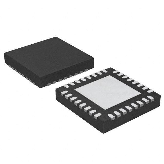
| 供应商器件封装 | 32-QFN(5x5) |
| 其它名称 | AS3911-BQFT-1K |
| 包装 | 带卷 (TR) |
| 封装/外壳 | 32-VFQFN 裸露焊盘 |
| 标准包装 | 1,000 |
| 特性 | ISO14443-A,ISO14443-B |
| 特色产品 | http://www.digikey.cn/product-highlights/cn/zh/ams-as3911-hf-rfid-reader-ic/3600 |
| 频率 | 13.56MHz |


- 商务部:美国ITC正式对集成电路等产品启动337调查
- 曝三星4nm工艺存在良率问题 高通将骁龙8 Gen1或转产台积电
- 太阳诱电将投资9.5亿元在常州建新厂生产MLCC 预计2023年完工
- 英特尔发布欧洲新工厂建设计划 深化IDM 2.0 战略
- 台积电先进制程称霸业界 有大客户加持明年业绩稳了
- 达到5530亿美元!SIA预计今年全球半导体销售额将创下新高
- 英特尔拟将自动驾驶子公司Mobileye上市 估值或超500亿美元
- 三星加码芯片和SET,合并消费电子和移动部门,撤换高东真等 CEO
- 三星电子宣布重大人事变动 还合并消费电子和移动部门
- 海关总署:前11个月进口集成电路产品价值2.52万亿元 增长14.8%


PDF Datasheet 数据手册内容提取
AS3911 NFC Initiator / HF Reader IC General Description The AS3911 is a highly integrated NFC Initiator / HF Reader IC. It includes the analog front end (AFE) and a highly integrated data framing system for ISO 18092 (NFCIP-1) initiator, ISO 18092 (NFCIP-1) active target, ISO 14443 A and B reader (including high bit rates) and FeliCa™ reader. Implementation of other standard and custom protocols is possible through using the AFE and implementing framing in the external microcontroller (Stream and Transparent modes). Compared with concurrent NFC devices designed with the mobile phone in mind, the AS3911 is positioned perfectly for the infrastructure side of the NFC system, where users need optimal RF performance and flexibility combined with low power. With ams unique Automatic Antenna Tuning technology, the device is optimized for applications with directly driven antennas. The AS3911 is alone in the domain of HF Reader ICs in that it contains two differential low impedance (1Ω) antenna drivers. The AS3911 includes several features, which make it incomparable for low power applications. It contains a low power capacitive sensor, which can be used to detect the presence of a card without switching on the reader field. Additionally, the presence of a card can also be detected by performing a measurement of amplitude or phase of signal on antenna LC tank and comparing it to stored reference. It also contains a low power RC oscillator and wake-up timer, which can be used to wake the system after a defined time period and check for the presence of a tag using one or more techniques of low power detection of card presence (capacitive, phase or amplitude). The AS3911 is designed to operate from a wide power supply range from 2.4V to 5.5V; peripheral interface IO pins support power supply range from 1.65V to 5.5V. OrderingInformation and ContentGuide appear at end of datasheet. ams Datasheet Page 1 [v2-11] 2016-Jun-13 DocumentFeedback
AS3911 − General Description Key Benefits & Features The benefits and features of AS3911, NFC Initiator / HF Reader IC are listed below: Figure 1: Added Value of Using AS3911 Benefits Features ISO 18092 (NFCIP-1) Active P2P NFC Active P2P support ISO14443 A, B and FeliCa (TM) High data transfer with ASK VHBR and fast Support of VHBR (3.4 Mbit/s PICC to PCD framing, 6.8 Mbit/s AFE SPI and PCD to PICC framing) 6μA consumption at sensing every 100ms Capacitive sensing - Wake-up Automatic Antenna Tuning system providing tuning of antenna Antenna tuning on the fly LC tank Stable modulation index at ASK modulation Automatic modulation index adjustment AM and PM (I/Q) demodulator channels with automatic No communication holes selection High output power for EMVCo readers Up to 1 W in case of differential output High Rx sensitivity User selectable and automatic gain control Transparent and Stream modes to implement MIFARE™ Classic Allows implementation of custom framings compliant or other custom protocols Multi Antenna support Possibility of driving two antennas in single ended mode Oscillator input capable of operating with 13.56 MHz or 27.12 Smaller Oscillator size MHz crystal with fast start-up Easy FIFO handling 10 M bit SPI with 96 bytes FIFO Wide supply voltage range from 2.4 V to 5.5 V Fits Temperature requirements for various Wide temperature range: -40°C to 125°C applications Small outline, good cooling through QFN 5mm x 5mm LD32 package exposed pad Page 2 ams Datasheet DocumentFeedback [v2-11] 2016-Jun-13
AS3911 − General Description Applications The AS3911 is suitable for a wide range of applications including: • EMV Payment • Access Control • NFC Infrastructure • Ticketing Block Diagram The functional blocks of this device for reference are shown below: Figure 2: AS3911 Block Diagram VDD_IO XTO XTI VDD XTAL Regulators PPOORR & & B Biaiass Oscillator LOGIC RFO1 Transmitter FIFO RFO2 SPI Level Control Phase & IRQ Shifters Logic A/D CAo/nDv erter Amplitude Converter MCU_CLK Detector SPI Interface RFI1 Receiver RFI2 TRIMx Framing External Field RC Wake-up Detector Oscillator Timer AS3911 Capacitor CSI Sensor CSO ams Datasheet Page 3 [v2-11] 2016-Jun-13 DocumentFeedback
AS3911 − Pin Assignment Pin Assignment The AS3911 pin assignments are described below. Figure 3: Pin Diagram AS3911 Pin Assignment: This figure shows the pin assignment and location viewed from top. K L /SS SCLK MOSI MISO MCU_C IRQ VSN_A CSI 32 31 30 29 28 27 26 25 VDD_IO 1 24 AGD CSO 2 23 RFI2 VSP_D 3 22 RFI1 XTO 4 AS3911 21 VSS XTI 5 20 TRIM2_0 VSN_D 6 19 TRIM1_0 VSP_A 7 18 TRIM2_1 VDD 8 17 TRIM1_1 9 10 11 12 13 14 15 16 F 1 2 F 3 3 2 2 P_R RFO RFO N_R M1_ M2_ M1_ M2_ VS VS TRI TRI TRI TRI Figure 4: Pin Description Pin Number Pin Name Pin Type Description 32-pin QFN 1 V Supply pad Positive supply for peripheral communication DD_IO 2 CSO Capacitor sensor output Analog 3 VSP_D Digital supply regulator output output 4 XTO Xtal oscillator output Analog input 5 XTI Xtal oscillator input / Digital input 6 VSN_D Supply pad Digital ground Analog 7 VSP_A Analog supply regulator output output 8 V Supply pad External positive supply DD Page 4 ams Datasheet DocumentFeedback [v2-11] 2016-Jun-13
AS3911 − Pin Assignment Pin Number Pin Name Pin Type Description 32-pin QFN 9 VSP_RF Supply regulator output for antenna drivers Analog 10 RFO1 output Antenna driver output 11 RFO2 12 VSN_RF Supply pad Ground of antenna drivers 13 TRIM1_3 14 TRIM2_3 15 TRIM1_2 16 TRIM2_2 Analog I/O Input to trim antenna resonant circuit 17 TRIM1_1 18 TRIM2_1 19 TRIM1_0 20 TRIM2_0 21 VSS Supply pad Ground, die substrate potential 22 RFI1 Analog input Receiver input 23 RFI2 24 AGD Analog I/O Analog reference voltage 25 CSI Analog input Capacitor sensor input 26 VSN_A Supply pad Analog ground 27 IRQ Interrupt request output Digital output 28 MCU_CLK Microcontroller clock output Digital output 29 MISO Serial Peripheral Interface data output / tristate 30 MOSI Serial Peripheral Interface data input 31 SCLK Digital input Serial Peripheral Interface clock 32 /SS Serial Peripheral Interface enable (active low) # VSS Exposed Pad Ground, die substract potential, connect to VSS on PCB Note(s): 1. Pins in bold have different functionality in comparison to the AS3910. ams Datasheet Page 5 [v2-11] 2016-Jun-13 DocumentFeedback
AS3911 − Absolute Maximum Ratings Absolute Maximum Ratings Stresses beyond those listed under Absolute Maximum Ratings may cause permanent damage to the device. These are stress ratings only. Functional operation of the device at these or any other conditions beyond those indicated under Operating Conditions is not implied. Exposure to absolute maximum rating conditions for extended periods may affect device reliability. Figure 5: Absolute Maximum Ratings Symbol Parameter Min Max Unit Comments Electrical Parameters V DC supply voltage -0.5 6.0 V DD DC_IO supply V -0.5 6.0 V DD_IO voltage Input pin voltage V -0.5 25.0 V INTRIM TRIM pins Input pin voltage for V peripheral -0.5 6.5 V IN communication pins Input pin voltage for V -0.5 6.0 V INA analog pins Input current I -100 100 mA JEDEC 78 scr (latch-up immunity) Drive capability of I 0 600 mA outmax output driver Electrostatic Discharge MIL 883 E method 3015 ±2 kV Electrostatic (Human Body Model) ESD discharge ±500 V Valid for Trimx.x pins (pins 13 - 20) Page 6 ams Datasheet DocumentFeedback [v2-11] 2016-Jun-13
AS3911 − Absolute Maximum Ratings Symbol Parameter Min Max Unit Comments Temperature Ranges and Storage Conditions T Storage temperature -55 125 °C strg IPC/JEDEC J-STD-020. The reflow peak soldering temperature (body temperature) is specified according Package body IPC/JEDEC J-STD-020 “Moisture/Reflow T 260 °C body temperature Sensitivity Classification for Non-hermetic Solid State Surface Mount Devices.” The lead finish for Pb-free leaded packages is matte tin (100% Sn). Relative humidity RH 5 85 % NC non-condensing Moisture sensitivity Represents a max. floor life time of 168 MSL 3 level hours Thermal Resistance @ 85°C room temperature, power θ Theta ja 36.4 C/W ja consumption 1W Note(s): 1. Please refer to Figure10 and Figure11 for typical operating characteristics of thermal resistance and max. power dissipation. ams Datasheet Page 7 [v2-11] 2016-Jun-13 DocumentFeedback
AS3911 − Electrical Characteristics Electrical Characteristics All limits are guaranteed. The parameters with min and max values are guaranteed with production tests or SQC (Statistical Quality Control) methods. Operating Conditions All defined tolerances for external components in this specification need to be assured over the whole operation condition range and also over lifetime. Figure 6: Operating Conditions Symbol Parameter Min Max Unit Comments V Positive supply voltage 2.4 5.5 V In case power supply is DD lower than 2.6V, PSSR cannot be improved using Peripheral internal regulators V communication supply 1.65 5.5 V DD_IO (minimum regulated voltage voltage is 2.4V) VSS Negative supply voltage 0 0 V Input pin voltage V 20 V INTRIM TRIM pins T Junction temperature -40 125 °C JUN Minimum RFI input signal definition is meant for NFC receive mode. In HF reader V RFI input amplitude 150 m 3 V RFI_A pp mode and NFC transmit mode, the recommended signal level is 2.5V pp RFO Driver current 0 500 mA DC/AC Characteristics for Digital Inputs and Outputs CMOS Inputs: Valid for input pins /SS, MOSI, and SCLK Figure 7: CMOS Inputs Symbol Parameter Min Max Unit V High level input voltage 0.7 * V V IH DD_IO V Low level input voltage 0.3 * V V IL DD_IO I Input leakage current 1 μA LEAK Page 8 ams Datasheet DocumentFeedback [v2-11] 2016-Jun-13
AS3911 − Electrical Characteristics CMOS Outputs: Valid for output pins MISO, IRQ and MCU_CLK, io_18=0 (See IO Configuration Register 2). Figure 8: CMOS Outputs Symbol Parameter Conditions Min Type Max Unit 0.9 * V High level input voltage V OH V I = 1mA DD_IO SOURCE I = 1mA SINK 0.1 * V Low level input voltage V OL V DD_IO C Capacitive load 50 pF L R Output Resistance 250 500 Ω O Pull-down can be enabled while MISO Pull-down resistance pin output is in tristate. R 10 kΩ PD MISO The activation is controlled by register setting. Electrical Specification V = 3.3V, Temperature 25°C unless noted otherwise. DD 3.3V supply mode, regulated voltages set to 3.4V, 27.12 MHz Xtal connected to XTO and XTI. Figure 9: Electrical Specification Symbol Parameter Min Typ Max Unit Comments Register 00 set to 0F (no clock on h h Supply current in MCU_CLK), register 01h set to 80h (3V I Power-down 0.7 2 μA supply mode), register 02 set to 00 PD h h mode register 03 set to 08 , other registers in h h default state. Register 00 set to 0F (no clock on h h MCU_CLK), register 01 set to 80 (3V h h Supply current in supply mode), register 02 set to 00 I initial NFC Target 3.5 7 μA h h NFCT register 03 set to 80 (enable NFC mode h h Target mode), other registers in default state. ams Datasheet Page 9 [v2-11] 2016-Jun-13 DocumentFeedback
AS3911 − Electrical Characteristics Symbol Parameter Min Typ Max Unit Comments Register 00 set to 0F (no clock on h h MCU_CLK), register 01 set to 80 (3V h h supply mode), register 02 set to 04 Supply current in h h IWU Wake-up mode 3.6 6 μA (enable Wake-up mode), register 03 set to 08 , register 31 set to 08 h h h h (100ms timeout, IRQ at every timeout), other registers in default state. Register 00 set to 0F (no clock on h h MCU_CLK), register 01 set to 80 (3V Capacitive sensor h h ICS supply current 1.1 2 mA supply mode), register 02h set to 00h, analog test mode 14, other registers in default state. Register 00 set to 0F (no clock on h h MCU_CLK), register 01 set to C0 (3V h h Supply current in supply mode, disable VSP_D), register I 5.4 7.5 mA RD Ready mode 02 set to 80 , register 03 set to 08 , h h h h other registers in default state, short VSP_A and VSP_D. Register 00 set to 0F , register 01 set h h h to C0 (3V supply mode, disable h VSP_D), register 02 set to E8 (one h h Supply current all channel Rx, enable Tx), register 03 set I 8.7 12.5 mA h AL active to 08, register 0B set to 00, register 27 h h set to FF (all RFO segments disabled), other registers in default state, short VSP_A and VSP_D. Register 00 set to 0F , register 01 set h h h to C0 (3V supply mode, disable h VSP_D), register 02 set to E8 (one h h Supply current all channel Rx, enable Tx), register 03 set I active, low power 6.8 10 mA h LP to 08, register 0B set to 80 (low power receiver mode h mode), register 27 set to FF (all RFO h segments disabled), other registers in default state, short VSP_A and VSP_D. Page 10 ams Datasheet DocumentFeedback [v2-11] 2016-Jun-13
AS3911 − Electrical Characteristics Symbol Parameter Min Typ Max Unit Comments I = 10 mA RFO The following measurement procedure which cancels resistance of measurement setup is used: • All driver segments are switched on, resistance is measured, RFO1 and RFO2 • All driver segments except the MSB R driver output 0.6 1.8 Ω RFO segment are switched on, resistance resistance is measured, • Difference between the two measurements is resistance of MSB segment, • Resistance of MSB segment divided by two is the value of R . RFO Using Load impedance lower than Load impedance Z 8 10 50 Ω minimum value can result in load across RFI1 & RFI2 permanent damage of the IC RFI input f =848 kHz, AM channel with peak V 0.5 mV SUB RFI sensitivity rms detector input stage selected. RFI input R 10 15 kΩ RFI resistance Power on Reset V 1.2 1.65 2.0 V POR voltage Register 00 set to 0F (no clock on h h MCU_CLK), register 01 set to C0 (3V h h supply mode, disable VSP_D), register V AGD voltage 1.4 1.5 1.6 V AGD 02 set to 80 , register 03 set to 08 , h h h h other registers in default state, short VSP_A and VSP_D. Manual regulator mode, regulated voltage set to 3.0V, measured on pin VSP_RF: register 00 set to 0F , register Regulated h h V 2.85 3.0 3.15 V REG voltage 01h set to 80h (3V supply mode), register 02 set to E8 (one channel Rx, h h enable Tx), register 2A set to D8 . h h 13.56MHz or 27.12MHz crystal R = 50 Ω max, load capacitance Oscillator start-up S TOSC time 0.65 0.7 10 ms according to crystal specification, IRQ is issued once the oscillator frequency is stable. ams Datasheet Page 11 [v2-11] 2016-Jun-13 DocumentFeedback
AS3911 − Typical Operating Characteristics Typical Operating Characteristics Thermal Resistance and Max. Power Dissipation Figure 10: TCASE vs. Power with Different Copper Area @ T = 25°C AMB Tcase(cid:3)vs(cid:3)Power(cid:3)QFN32(cid:3)(cid:3)with(cid:3)different(cid:3)copper(cid:3)area.(cid:3)Tamb(cid:3)=(cid:3)25°C 100 90 0x0mm 80 10x10mm 70 20x20mm C] 30x30mm e[°(cid:3) 60 40x40mm as Tc 50x50mm 50 60x60mm 70x70mm 40 30 20 0 0,5 1 1,5 2 2,5 Power(cid:3)Dissipation(cid:3)[W] Figure 11: RthCA vs. Copper Area Rth_CA [K/W] vs Copper Area 100 90 80 70 W] 60 K/ A [ 50 C _ h Rt 40 30 20 10 0 0 10 20 30 40 50 60 Area [cm^2] Page 12 ams Datasheet DocumentFeedback [v2-11] 2016-Jun-13
AS3911 − Detailed Description Detailed Description The circuit diagram in Figure2 shows the AS3911 building blocks. Figure 12: Minimum Configuration with Single Sided Antenna Driving Including EMC Filter +1.6V ~ +5.5V +2.4V ~ +5.5V VDD_IO VDD AGD /SS MISO VSS μC MOSI SCLK VSP_A IRQ MCU_CLK VSN_A VSP_D XTI VSN_D AS3911 XTO VSP_RF TRIM1_x VSN_RF TRIM2_x RF01 RF02 Antenna CSO Coil CSI RFI1 RFI2 Figure 13: Minimum Configuration with Differential Antenna Driving Including EMC Filter +1.6V ~ +5.5V +2.4V ~ +5.5V VDD_IO VDD AGD /SS MISO VSS µC MOSI SCLK VSP_A IRQ MCU_CLK VSN_A VSP_D XTI VSN_D AS3911 XTO VSP_RF TRIM1_x VSN_RF TRIM2_x RF01 RF02 CSO RFI1 Antenna CSI Coil RFI2 ams Datasheet Page 13 [v2-11] 2016-Jun-13 DocumentFeedback
AS3911 − Detailed Description Transmitter The transmitter incorporates drivers which drive external antenna through pins RFO1 and RFO2. Single sided and differential driving is possible. The transmitter block additionally contains a sub-block which modulates transmitted signal (OOK or configurable AM modulation). The AS3911 transmitter is indented to directly drive antennas (without 50Ω cable, usually antenna is on the same PCB). Oper- ation with 50Ω cable is also possible, but in that case some of the advanced features are not possible. By applying FFh to the register 27h, the output driver are in tristate. Receiver The receiver detects transponder modulation superimposed on the 13.56MHz carrier signal. The receiver contains two receive chains (one for AM and another for PM demodulation) which are composed of a peak detector followed by two gain and filtering stages and a final digitizer stage. The filter characteristics are adjusted to optimize performance over different ISO modes and bit rates (sub-carrier frequencies from 212 kHz to 6.8 MHz are supported). The receiver chain inputs are RFI1 and RFI2 pins; output of digitizer stage is demodulated sub-carrier signal. The receiver chain incorporates several features which enable reliable operation in challenging phase and noise conditions. Phase and Amplitude Detector The phase detector is observing the phase difference between the transmitter output signals (RFO1 and RFO2) and the input signals RFI1 and RFI2. Signals RFI1 and RFI2 are proportional to the signal on the antenna LC tank. RFI1 and RFI2 signals are also used to run the self-mixer which generates output proportional to their amplitude. The phase detector and self-mixer blocks are used for several purposes: • PM demodulation by observing RFI1 and RFI2 phase variation (LF signal is fed to the Receiver) • Average phase difference between RFOx pins and RFIx pins is used to check antenna tuning • Output of mixer is used to measure amplitude of signal present on pins RFI1 and RFI2 A/D Converter The AS3911 contains a built in A/D Converter. Its input can be multiplexed from different sources and is used in several applications (measurement of RF amplitude and phase, calibration of modulation depth…). The result of A/D conversion is stored in a register which can be read through the SPI interface. Page 14 ams Datasheet DocumentFeedback [v2-11] 2016-Jun-13
AS3911 − Detailed Description Capacitive Sensor The Capacitive sensor is used to implement low power detection of transponder presence. Capacitive sensor performs measurement of capacitance between its two electrodes. Presence of an object (card, hand) changes the capacitance. During calibration the reference capacitance, which represents parasitic capacitance of environment is stored. In normal operation capacitance is periodically measured and compared to stored reference value. When the measured capacitance is larger than stored reference value (threshold value can be defined in a register) an interrupt is sent to external controller. External Field Detector The External Field Detector is a low power block which is used in NFC mode to detect presence of external RF field. It supports two different detection thresholds, Peer Detection Threshold and Collision Avoidance Threshold. Peer Detection Threshold is used in the NFCIP-1 target mode to detect presence of initiator field. It is also used in active communication initiator mode to detect activation of target field. Collision Avoidance Threshold is used to detect a presence of RF field during NFCIP-1 RF Collision Avoidance procedure. Quartz Crystal Oscillator The quartz crystal oscillator can operate with 13.56 MHz and 27.12 MHz crystals. At start-up the transconductance of the oscillator is increased to achieve fast start-up. Since the start-up time varies depending on crystal type, temperature and other parameters, the oscillator amplitude is observed and an interrupt is sent when stable operation is reached to inform the controller that the clock signal is stable and reader field can be switched on. The use of 27.12 MHz crystal is mandatory in case VHBR framing is used. It also provides a clock signal to the external microcontroller (MCU_CLK) according to setting in the control register. Power Supply Regulators Integrated power supply regulators ensure high power supply rejection of a complete reader system. In case PSRR of the reader system has to be improved, the command Adjust Regulators is sent. As result of this command, the power supply level of V DD is measured in maximum load conditions and the regulated voltage reference is set 250 mV below this measured level to assure a stable regulated supply. The resulting regulated voltage is stored in a register. It is also possible to define regulated voltage by writing a configuration register. In order to decouple any noise sources from different parts of IC there are three regulators integrated with separated external blocking capacitors (regulated voltage of all is the same in 3.3V supply mode). ams Datasheet Page 15 [v2-11] 2016-Jun-13 DocumentFeedback
AS3911 − Detailed Description One regulator is for the analog blocks, one for digital blocks, there is also a separate one for the antenna drivers. In case of low cost applications some (or all) regulators may not be used to save on external components. This block additionally generates a reference voltage for the analog processing (AGD - analog ground). This voltage also has an associated external buffer capacitor. POR and Bias This block contains the bias current and voltage generator which provides bias currents and reference voltages to all other blocks. It also incorporates a Power on Reset (POR) circuit which provides a reset at power-up and at low supply levels. RC Oscillator and Wake-up Timer The AS3911 includes several possibilities of low power detection of a card presence (capacitive sensor, phase measurement, amplitude measurement). RC oscillator and register configurable Wake-up timer are used to schedule periodic detection. When presence of a card is detected an interrupt is sent to controller. ISO14443 and NFCIP-1 Framing This block performs framing for receive and transmit according to the selected ISO mode and bit rate settings. In reception it takes demodulated sub-carrier signal from Receiver. It recognizes the SOF, EOF and data bits, performs parity and CRC check, organizes the received data in bytes and places them in the FIFO. During transmit, it operates inversely, it takes bytes from FIFO, generates parity and CRC bits, adds SOF and EOF and performs final encoding before passing modulation signal to transmitter. In Transparent mode, the framing and FIFO are bypassed, the digitized sub-carrier signal, which is Receiver output, is directly sent to MISO pin, signal applied to MOSI pin is directly used to modulate the transmitter. FIFO The AS3911 contains a 96 byte FIFO. Depending on the mode, it contains either data which has been received or data which is to be transmitted. Control Logic The control logic contains I/O registers which define operation of device. Page 16 ams Datasheet DocumentFeedback [v2-11] 2016-Jun-13
AS3911 − Application Information SPI Interface A 4-wire Serial Peripheral Interface (SPI) is used for communication between external microcontroller and the AS3911. Application Information Operating Modes The AS3911 operating mode is defined by the contents of the Operation Control Register. At power-up all bits of the Operation Control Register are set to 0, the AS3911 is in Power-down mode. In this mode AFE static power consumption is minimized, only the POR and part of the bias are active, the regulators are transparent and are not operating. The SPI is still functional in this mode so all settings of ISO mode definition and configuration registers can be done. Control bit en (bit 7 of the Operation Control Register) is controlling the quartz crystal oscillator and regulators. When this bit is set, the device enters in Ready mode. In this mode the quartz crystal oscillator and regulators are enabled. An interrupt is sent to inform the microcontroller when the oscillator frequency is stable. Enable of Receiver and Transmitter are separated so it is possible to operate one without switching on the other (control bits rx_en and tx_en). In some cases this may be useful, in case the reader field has to be maintained and there is no transponder response expected receiver can be switched-off to save current. Another example is NFCIP-1 active communication receive mode in which RF field is generated by the initiator and only Receiver operates. Asserting the Operation Control Register bit wu while the other bits are set to 0 puts the AS3911 into the Wake-up mode which is used to perform low power detection of card presence. In this mode the low power RC oscillator and register configurable Wake-up timer are used to schedule periodic measurement(s). When a difference to the predefined reference is detected an interrupt is sent to wake-up the micro. Capacitive sensor, phase measurement and amplitude measurement are available. Transmitter The Transmitter contains two identical push-pull driver blocks connected to the pins RFO1 and RFO2. These drivers are differentially driving external antenna LC tank. It is also possible to operate only one of the two drivers by setting the IO Configuration Register 1 bit single. Each driver is composed of 8 segments having binary weighted output resistance. The MSB segment typical ON resistance is 2Ω, when all segments are turned on; the output resistance is typically 1Ω. Usually all segments are turned on to define the normal transmission (non-modulated) level. ams Datasheet Page 17 [v2-11] 2016-Jun-13 DocumentFeedback
AS3911 − Application Information It is also possible to switch off certain segments when driving the non-modulated level to reduce the amplitude of signal on the antenna and/or to reduce the antenna Q factor without making any hardware changes. The RFO Normal Level Definition Register defines which segments are turned on to define the normal transmission (non-modulated) level. Default setting is that all segments are turned on. Using the single driver mode the number and therefore the cost of the antenna LC tank components is halved, but also the output power is reduced. In single mode it possible to connect two antenna LC tanks to the two RFO outputs and multiplex between them by controlling the IO Configuration Register 1 bit rfo2. In order to transmit the data the transmitter output level needs to be modulated. The AM and OOK modulation are supported. The type of modulation is defined by setting the bit tr_am in the Auxiliary Definition Register. For the operation modes supported by the AS3911 framing the setting of modulation type is done automatically by sending direct command Analog Preset. During the OOK modulation (for example ISO14443A) the Transmitter drivers stop driving the carrier frequency; drivers are frozen in state before the modulation. As consequence the amplitude of the antenna LC tank oscillation decays, the time constant of the decay is defined with the LC tank Q factor. The decay time in case of OOK modulation can be shortened by asserting the Auxiliary Definition Register bit ook_hr. When this bit is set to logic one the drivers are put in tristate during the OOK modulation. AM modulation (for example ISO14443B) is done by increasing the output driver impedance during the modulation time. This is done by reducing the number of driver segments which are turned on. The AM modulated level can be automatically adjusted to the target modulation depth by defining the target modulation depth in the AM Modulation Depth Control Register and sending the Calibrate Modulation Depth direct command. Please refer to AM Modulation Depth: Definition and Calibration for further details. Slow Transmitter Ramping When transmitter is enabled it starts to drive the antenna LC tank with full power, the ramping of field emitted by antenna is defined by antenna LC tank Q factor. However there are some reader systems where the reader field has to transition with a longer transition time when it is enabled. The STIF (Syndicat des transports d'Ile de France) specification requires a transition time from 10% to 90% of field longer than or equal to 10 μs. The AS3911 supports that feature. It is realized by collapsing VSP_RF regulated voltage when transmitter is disabled and ramping it when transmitter is enabled. Typical transition time is 15 μs at 3V supply and 20 μs at 5V supply. Page 18 ams Datasheet DocumentFeedback [v2-11] 2016-Jun-13
AS3911 − Application Information Procedure to implement the slow transition: • When transmitter is disabled set IO Configuration Register 2 bit slow_up to 1. Keep this state at least 2 ms to allow discharge of VSP_RF. • Enable transmitter, its output will ramp slowly. • Before sending any command set the bit slow_up back to 0. Receiver The receiver performs demodulation of the transponder sub-carrier modulation which is superimposed on the 13.56MHz carrier frequency. It performs AM and/or PM demodulation, amplification, band-pass filtering and digitalization of sub-carrier signals. Additionally it performs RSSI measurement, automatic gain control (AGC) and Squelch function. In typical application the Receiver inputs RFI1 and RFI2 are outputs of capacitor dividers connected directly to the terminals of antenna coil. Such concept assures that the two input signals are in phase to the voltage on antenna coil. Care has to be taken during design of capacitive divider that the RFI1 and RFI2 input signal pp value does not exceed the VSP_A supply voltage. Receiver comprises two complete receive channels for AM demodulation and PM demodulation. In case both channels are active the selection of channel used for reception framing is done automatically by receive framing logic. The receiver is switched on when Operation Control Register bit rx_en is set to one. Additionally the Operation Control Register contains bits rx_chn and rx_man; rx_chn defines whether both, AM and PM, demodulation channels will be active or only one of them, while bit rx_man defines the channel selection mode in case both channels are active (automatic or manual). Operation of the Receiver is controlled by four Receiver Configuration registers. The operation of the receiver is additionally controlled by the signal rx_on which is set high when modulated signal is expected on the receiver input. This signal is used to control RSSI and AGC and also enables processing of receiver output by Framing logic. Signal rx_on is automatically set high after Mask Receive timer expires. Signal rx_on can also be directly controlled by the controller by sending direct commands Mask Receive Data and Unmask Receive Data. Figure14 illustrates the Receiver block diagram. Demodulation Stage First stage performs demodulation of transponder sub-carrier response signal, which is superimposed on HF field carrier. Two different blocks are implemented for AM demodulation: Peak Detector and AM demodulator mixer. The choice of the demodulator, which is used, is made by the Receiver Configuration Register 1 bit amd_sel. ams Datasheet Page 19 [v2-11] 2016-Jun-13 DocumentFeedback
AS3911 − Application Information Peak detector performs AM demodulation using peak follower. Both, the positive and negative peaks are tracked to suppress common mode signal. It is limited in speed; it can operate for sub-carrier frequencies up to fc/8 (1700 kHz). It has demodulation gain G = 0.7. Its input is taken from one demodulator input only (usually RFI1). AM demodulator mixer uses synchronous rectification of both receiver inputs (RFI1 and RFI2). Its gain is G = 0.55. Mixer demodulator is optimized for VHBR sub-carrier frequencies. (fc/8 and higher). For sub-carrier frequency fc/8 (1700 kHz) both peak follower and mixer can be used, while for fc/4 and fc/2 are supported only by mixer. By default the Peak detector is used, for data rates fc/8 and higher use of mixer is automatically preset by sending direct command Analog Preset. PM demodulation is also done by a mixer. The PM demodulator mixer has differential outputs with 60mV differential signal for 1% phase change (16.67 mV per degree). Its operation is optimized for sub-carrier frequencies up to fc/8 (1700 kHz). In case the demodulation is done externally of the AS3911 it is possible to multiplex the LF signals applied to pins RFI1 and RFI2 directly to the gain and filtering stage by selecting the Receiver Configuration Register 2 bit lf_en. Figure 14: Receiver Block Diagram rec1<7:6> AM rec2<6:5> Demodulator Mixer rec4<7:4> rec3<7:5> M AGC RSSI_AM<3:0> Squelch U RSSI X RF_IN1 digital Peak Detector sub-carrier RX_on RF_IN2 sg_on rec4<3:0> rec3<4:2> AGC RSSI_PM<3:0> PM Squelch Demodulator RSSI digital Mixer sub-carrier rec3<2:0> rec1<5:3> Demodulation AC coupling Low-pass High-pass Digitizing stage + 1stgain stage + 2ndgain stage + 3rdgain stage stage Page 20 ams Datasheet DocumentFeedback [v2-11] 2016-Jun-13
AS3911 − Application Information Filtering and Gain Stages The receiver chain has band pass filtering characteristics. Filtering is optimized to pass sub-carrier frequencies while rejecting carrier frequency and low frequency noise and DC component. Filtering and gain is implemented in three stages where the first and the last stage have the first order high pass characteristics, while the mid stage has second order low pass characteristic. Gain and filtering characteristics can be optimized for current application by writing the Receiver Configuration Register 1 (filtering), Receiver Configuration Register 3 (gain in first stage) and Receiver Configuration Register 4 (gain in second and third stage). Gain of first stage is about 20dB and can be reduced in six 2.5 dB steps. There is also a special boost mode available, which boosts the maximum gain for additional 5.5 dB. In case of VHBR (fc/8 and fc/4) the gain is lower. The first stage gain can only be modified by writing Receiver Configuration Register 3. The default setting of this register is the minimum gain. Default first stage zero is located at 60 kHz, it can also be lowered to 40kHz or 12 kHz by writing option bits in the Receiver Configuration Register 1. The control of the first and third stage zeros is done with common control bits (see Figure16). Gain in the second and third stage is 23 dB and can be reduced in six 3 dB steps. Gain of these two stages is included in AGC and Squelch loops or can be manually set in Receiver Configuration Register 4. Sending of direct command Reset Rx Gain is necessary to reset the AGC, Squelch and RSSI block. Sending this command clears the current Squelch setting and loads the gain reduction configuration from Receiver Configuration Register 4 into the internal shadow registers of AGC/Squelch block. Second stage has a second order low pass filtering characteristic, the pass band is adjusted according to sub-carrier frequency using the bits lp2 to lp0 of the Receiver Configuration Register 1. See Figure15 for -1dB cut-off frequency for different settings. Figure 15: Low Pass Control rec1<5> lp2 rec1<4> lp1 rec1<3> lp0 -1 dB point 0 0 0 1200 kHz 0 0 1 600 kHz 0 1 0 300 kHz 1 0 0 2 MHz 1 0 1 7 MHz Other Not used ams Datasheet Page 21 [v2-11] 2016-Jun-13 DocumentFeedback
AS3911 − Application Information Figure 16: First and Third Stage Zero Setting First Stage Third Stage rec1<2> h200 rec1<1> h80 rec1<0> z12k Zero Zero 0 0 0 60 kHz 400 kHz 1 0 0 60 kHz 200 kHz 0 1 0 40 kHz 80 kHz 0 0 1 12 kHz 200 kHz 0 1 1 12 kHz 80 kHz 1 0 1 12 kHz 200 kHz Other Not used Figure17 provides information on the recommended filter settings. For all supported operation modes and receive bit rates there is an automatic preset defined, additionally some alternatives are listed. Automatic preset is done by sending direct command Analog Preset. There is no automatic preset for Steam and Transparent modes. Since selection of filter characteristics also modifies gain, the gain range for different filter settings is also listed. Figure 17: Receiver Filter Selection and Gain Range Gain [dB] > 3> > > > rec1<5:lp<2:0 rec1<2h200 rec1<1h80 rec1<0z12k Max All Min1 Max23 Max1 Min23 Min All With Boost Comment Automatic preset for ISO14443A fc/128 000 0 0 0 43.4 28 26.4 11 49.8 and NFC Forum Type 1 Tag Automatic preset for ISO14443B fc/128 000 1 0 0 44 29 27.5 12 49.7 ISO14443 fc/64 Recommended for 424/484 kHz 001 1 0 0 44.3 29 27 11.7 49.8 sub-carrier Alternative choice for ISO14443 fc/32 and 000 0 1 0 41.1 25.8 23.6 8.3 46.8 fc/16 Automatic preset for ISO14443 fc/32 and 100 0 1 0 32 17 17.2 2 37.6 fc/16 Alternative choice for fc/8 (1.7 kbit/s) 100 0 0 0 32 17 17.2 2 37.6 Alternative choice for fc/8 (1.7 kbit/s) Page 22 ams Datasheet DocumentFeedback [v2-11] 2016-Jun-13
AS3911 − Application Information Gain [dB] > 3> > > > rec1<5:lp<2:0 rec1<2h200 rec1<1h80 rec1<0z12k Max All Min1 Max23 Max1 Min23 Min All With Boost Comment Automatic preset FeliCa (fc/64, fc/32) 000 0 1 1 41.1 25.8 23.6 8.3 46.8 Alternative choice for ISO14443 fc/32 and fc/16 101 0 1 0 30 20 12 2 34 Alternative choice for fc/8 and fc/4 101 1 0 0 30 20 12 2 34 Automatic preset for fc/8 and fc/4 Automatic preset for NFCIP-1 (initiator and 000 1 0 1 36.5 21.5 24.9 9.9 41.5 target) Digitizing Stage Digitizing stage is producing a digital form of sub-carrier signal which is output of Receiver and input to Framing Logic. It is a window comparator with adjustable digitizing window (five possible settings, 3 dB steps, adjustment range from ±33 mV to ±120 mV). Adjustment of the digitizing window is included in AGC and Squelch loops or can be manually set in Receiver Configuration Register 4. AGC, Squelch and RSSI As mentioned above second and third gain stage gain and the Digitizing stage digitizing window are included in AGC and Squelch loops. Eleven settings are available, default state features minimum digitizer window and maximum gain, first four steps increase the digitizer window in 3 dB steps, next six steps additionally reduce the gain in 2nd and 3rd gain stage also in 3 dB steps. The initial setting with which Squelch and AGC start is defined in Receiver Configuration Register 4. The Gain Reduction State Register displays the actual state of gain which results from Squelch, AGC and initial settings in Receiver Configuration Register 4. Squelch This feature is designed for operation of receiver in noisy environment. The noise can come from tags in which processing of data sent by the reader is going on and an answer is being prepared. Noise can also be generated by noisy environment. This noise may be misinterpreted as start of transponder response which results in decoding error. During execution of the Squelch procedure the output of Digitizing comparator is observed. In case there are more than two transitions on this output in 50 μs time period, gain is reduced for 3 dB and output is observed during next 50 μs. This procedure is repeated until number of transitions in 50 μs is lower or equal to 2 or until maximum gain reduction is reached. ams Datasheet Page 23 [v2-11] 2016-Jun-13 DocumentFeedback
AS3911 − Application Information This setting is cleared by sending direct command Reset Rx Gain. There are two possibilities of performing squelch: automatic mode and using direct command Squelch. • Automatic mode is started in case bit sqm_dyn in the Receiver Configuration Register 2 is set. It is activated automatically 18.88 μs after end of Tx and is terminated with Mask Receive timer expire. This mode is primarily intended to suppress noise generated by tag processing during the time when the tag response is not expected (covered by Mask Receive timer). • Command Squelch is accepted in case it is sent when signal rx_on is low. It can be used in case the time window in which noise is present is known by the controller. AGC AGC (automatic gain control) is used to reduce gain to keep receiver chain out of saturation. In case gain is properly adjusted the demodulation process is also less influenced by system noise. AGC action starts when signal rx_on is asserted high and is reset when it is reset to low. At high to low transitions of the rx_on the state of the receiver gain is stored in the Gain Reduction State Register, therefore reading this register later gives the information of the gain setting used during last reception. When AGC is switched on receiver gain is reduced so that the input to digitizer stage is not saturated. The AGC system comprises a window comparator which has its window 3.5 times larger than window of digitalization window comparator. When the AGC function is enabled gain is reduced until there are no transitions on its output. Such procedure assures that the input to digitalization window comparator is less than 3.5 times larger than its window. AGC operation is controlled by the control bits agc_en, agc_m and agc_fast in the Receiver Configuration Register 2. Bit agc_en enables the AGC operation; bit agc_m defines the AGC mode while bit agc_alg define the AGC algorithm. Two AGC modes are available, AGC can operate during complete Rx process (as long as signal rx_on is high) or it can be enabled only during first eight sub-carrier pulses. Two AGC algorithms are available; AGC can either start by presetting of code 4 (max digitizer window, max gain) or by h resetting the code to 0 (min digitizer window, max gain). h Algorithm with preset code is faster, therefore it is recommended for protocols with short SOF (like ISO14443A fc/128). Default AGC settings are: AGC is enabled, AGC operates during complete Rx process, algorithm with preset is used. Page 24 ams Datasheet DocumentFeedback [v2-11] 2016-Jun-13
AS3911 − Application Information RSSI The receiver also performs the RSSI (Received Signal Strength Indicator) measurement of both channels. RSSI measurement is started after rising edge of rx_on. It stays active while signal rx_on is high; while rx_on is low it is frozen. It is a peak hold system; the value can only increase from initial zero value. Every time the AGC reduces the gain the RSSI measurement is reset and starts from zero. Result of RSSI measurements is 4-bit value which can be observed by reading the RSSI Display Register. The LSB step is 2.8 dB, the maximum code is D (13 ). h d Since the RSSI measurement is of peak hold type the RSSI measurement result does not follow any variations in the signal strength (the highest value will be kept). In order to follow RSSI variation it is possible to reset RSSI bits and restart the measurement by sending direct command Clear RSSI. Receiver in NFCIP-1 Active Communication Mode There are several features built in receiver to enable reliable reception of active NFCIP-1 communication. All these settings are automatically preset by sending direct command Analog Preset after the NFCIP-1 mode has been configured. In addition to filtering options there are two NFC specific configuration bits stored in the Receiver Configuration Register 3. Bit lim enables clipping circuits which are positioned after first and second gain stages. The intention of clipping circuits is to limit the signal level for the following filtering stage (in case the NFC peer is close the input signal level can be quite high). Bit rg_nfc forces gain reduction of second and third filtering stage to -6dB while keeping the digitizer comparator window at maximum level. Capacitive Sensor The Capacitive Sensor block provides a possibility of low power detection of tag presence. The capacitive measurement system comprises two electrodes. One is excitation electrode emitting electrical field of a fixed frequency in range of few hundred kHz (CSO) and the second one is the sensing electrode (CSI). The amount of charge gen- erated in sensing electrode represents the capacitance be- tween the two electrodes. Capacitive sensor electrodes are tol- erant to parasitic capacitance to ground (up to 25 pF) and to input leakage (up to 1 MΩ). Since the charge on the sensing electrode is generated with the frequency of excitation electrode, synchronous rectifier is used to detect it. This ensures good rejection of interference and high tolerance to parasitic capacitances (to all nodes except the excitation electrode). ams Datasheet Page 25 [v2-11] 2016-Jun-13 DocumentFeedback
AS3911 − Application Information Capacitive sensor system depicted on figure below uses a syn- chronous rectifier to convert the AC charge generated by the excitation signal on the sensing electrode. This yields a DC out- put voltage, which is linearly proportional to the capacitance between the excitation and sensing electrode. The output DC voltage is converted by an AD converter in absolute mode. Re- sult is stored in the A/D Converter Output Register (see also A/D Converter). Figure 18: Capacitive Sensor Block Diagram CSO Oscillator CSI A/D Synchronous Converter Rectifier Any conductive object (human hand or tag's antenna windings) approaching the two electrodes changes the capacitance between the excitation and sensing electrode as it 'shortens' the distance between the two by providing conductance on the part of the path between the two electrodes. Capacitance measurement is started by sending direct command Measure Capacitance. The AS3911 can also be configured to periodically wake-up and perform the capacitance measurement. The result is compared to a stored reference or to an average of previous measurements and in case the difference is greater than a predefined value an IRQ is triggered to wake-up the controller (see also Wake-Up Mode). Capacitor sensor gain can be adjusted by setting in Capacitive Sensor Control Register. Default gain is 2.8V/pF typ., maximum gain is 6.5V/pF typ. Since LSB of AD converter corresponds to approximately 7.8mV, the default gain results in sensitivity of 2.8 fF/LSB (1.2 fF/LSB maximum). Capacitance measurement duration is 200 μs, current consumption during measurement is 1.1 mA typ. In case capacitive measurement is performed every 100 ms in Wake-up mode the resulting typical average consumption is 5.8μA (3.6μA is standby consumption in Wake-up mode). Page 26 ams Datasheet DocumentFeedback [v2-11] 2016-Jun-13
AS3911 − Application Information Capacitor Sensor Calibration Capacitor sensor comprises calibration unit internally compensates the parasitic capacitances between CSI and CSO, thus leaving full measurement range for information about capacitance variation. 5 bits are used to control the calibration, minimum calibration step is 0.1pF, calibration range is 3.1pF. Calibration can be done manually by writing Capacitive Sensor Control Register or automatically by sending direct command Calibrate Capacitive Sensor. The status of Calibrate Capacitive Sensor command and resulting calibration value are stored in the Capacitive Sensor Display Register. In order to avoid interference of Capacitive Sensor with Xtal oscillator and reader magnetic field and to assure repetitive results it is strongly recommended to perform capacitance measurement and calibration in Power-down mode only. Wake-Up Mode Asserting the Operation Control Register bit wu while the other bits are set to 0 puts the AS3911 into the Wake-up mode which is used to perform low power detection of card presence. The AS3911 includes several possibilities of low power detection of a card presence (capacitive sensor, phase measurement, amplitude measurement). Low power 32kHz RC oscillator and register configurable Wake-up timer are used to schedule periodic detection. Usually the presence of a card is detected by so called polling. In this process the reader is periodically turned on and the controller activates the protocol to check whether a card is present. Such procedure consumes a lot of energy since reader field has to be turned on for 5ms before a command can be issued. Low power detection of card presence is performed by detecting a change in reader environment, which is produced by presence of a card. When a change is detected, an interrupt is sent to the controller. As a result, the controller can activate the protocol for tag detection. In the Wake-up mode the AS3911 periodically performs the configured measurements and sends an IRQ to the controller, which is in deep sleep to minimize the current consumption, only when a difference to the build in reference is detected. Detection of card presence can be done by performing phase, amplitude and capacitive sensor measurements. Presence of a card close to the reader antenna coil produces due to the magnetic coupling of the two coils a change of the antenna LC tank signal phase and amplitude. ams Datasheet Page 27 [v2-11] 2016-Jun-13 DocumentFeedback
AS3911 − Application Information The reader field activation time needed to perform the phase or the amplitude measurement is extremely short (~20μs) comparing to the activation time needed to send a protocol activation command. Additionally the power level during the measurement can be lower than the power level during normal operation since the card does not have to be powered to produce the coupling effect. The emitted power can be reduced by increasing the RFO Normal Level Definition Register. Capacitance Sensor detects a change of the parasite capacitance between the two excitation electrodes which is caused by a card antenna and a hand holding it. See Capacitive Sensor for a detailed information on the capacitive sensor. The registries on locations from 31 to 3D are dedicated to h h Wake-up configuration and display. The Wake-Up Timer Control Register is the main Wake-up mode configuration register. The timeout period between the successive detections and the measurements which are going to be used are selected in this register. Timeouts in the range from 10 ms to 800 ms are available, 100 ms is the default value. Any combination of available measurements can be selected (one, two or all of them). The following twelve registers (32 to 3D ) are configuring the h h three possible detection measurements and storing the results, four registers are used for each measurement. An IRQ is sent when the difference between a measured value and reference value is larger than configured threshold value. There are two possibilities how to define the reference value: • The AS3911 can calculate the reference based on previous measurements (auto-averaging) • The controller determines the reference and stores it in a register The first register in the series of four is the Measurement Configuration Register (see for e.g. Amplitude Measurement Configuration Register). The difference to reference which triggers the IRQ, the method of reference value definition and the weight of last measurement result in case of auto-averaging are defined in this register. The next register is storing the reference value in case the reference is defined by the controller. The following two registers are display registers. The first one stores the auto-averaging reference; the second one stores the result of the last measurement. Wake-up mode configuration registers have to be configured before wake-up mode is actually entered. Any modification of Wake-up mode configuration while it is active may result in unpredictable behavior. Page 28 ams Datasheet DocumentFeedback [v2-11] 2016-Jun-13
AS3911 − Application Information Auto-Averaging In case of auto-averaging the reference value is recalculated after every measurement. The last measurement value, the old reference value and the weight are used in this calculation. The following formula is used to calculate the new reference value. MeasuredValue–OldAverage (EQ1) NewAverage = OldAverage+-------------------------------------------------------------------------------- Weight The calculation is done on 10 bits to have sufficient precision. The auto-averaging process is initialized when Wake-up mode is first time entered after initialization (power-up or using Set Default command). The initial value is taken from the Measurement Display Register (for example Amplitude Measurement Display Register) until the content of this register is not zero. Every Measurement Configuration register contains a bit which defines whether the measurement which causes an interrupt is taken in account for the average value calculation (for example bit am_aam of the Amplitude Measurement Reference Regis- ter). Quartz Crystal Oscillator The quartz crystal oscillator can operate with 13.56 MHz and 27.12 MHz crystals. The operation of quartz crystal oscillator is enabled when the Operation Control Register bit en is set to one. An interrupt is sent to inform the microcontroller when the oscillator frequency is stable (see Main Interrupt Register). The status of oscillator can be observed by observing the Auxiliary Display Register bit osc_ok. This bit is set to ‘1’ when oscillator frequency is stable. The oscillator is based on an inverter stage supplied by controlled current source. A feedback loop is controlling the bias current in order to regulate amplitude on XTI pin to 1V . pp This feedback assures reliable operation even in case of low quality crystals with R up to 50 Ω. In order to enable a fast reader s start-up an interrupt is sent when oscillator amplitude exceeds 750 mV . pp Division by two assures that 13.56MHz signal has a duty cycle of 50% which is better for the Transmitter performance (no PW distortion). Use of 27.12MHz crystal is therefore recommended for better performance. In case of 13.56 MHz crystal, the bias current of stage which is digitizing oscillator signal is increased to assure as low PW distortion as possible. Please note that in case of VHBR reception (bit rates fc/8 and above) it is mandatory to use the 27.12MHz crystal since high frequency clock is needed for receive framing. ams Datasheet Page 29 [v2-11] 2016-Jun-13 DocumentFeedback
AS3911 − Application Information The oscillator output is also used to drive a clock signal output pin MCU_CLK), which can be used by the external microcontroller. The MCU_CLK pin is configured in the IO Configuration Register 2. Timers The AS3911 contains several timers which eliminate the need to run counters in the controller, thus reducing the effort of the controller code implementation and improve portability of code to different controllers. Every timer has one or more associated configuration registers in which the timeout duration and different operating modes are defined. These configuration registers have to be set while the corresponding timer is not running. Any modification of timer configuration while the timer is active may result in unpredictable behavior. All timers except the Wake-up timer are stopped by direct command Clear. Exception: In case bit nrt_emv in the General Purpose and No-Response Timer Control Register is set to one, the No-response timer is not stopped. Mask Receive Timer and No-Response Timer Mask Receive Timer and No-response Timer are both automatically started at the end of transmission (at the end of EOF). Mask Receive Timer The Mask Receive Timer is blocking the Receiver and reception process in framing logic by keeping the rx_on signal low after the end of Tx during the time the tag reply is not expected. While the Mask Receive timer is running, the Squelch is automatically turned on (if enabled). Mask receive timer does not produce an IRQ. The Mask Receive Timer timeout is configured in the Mask Receive Timer Register. In the NFCIP-1 active communication mode the Mask receive timer is started when the peer NFC device (a device with which communication is going on) switches on its field. The Mask Receive timer has a special use in the low power Initial NFC Target Mode. After the initiator field has been detected the controller turns on the oscillator, regulator and receiver. Mask Receive timer is started by sending direct command Start Mask-receive Timer. After the Mask Receive Timer expires the receiver output starts to be observed to detect start of the initiator message. In this mode the Mask Receive Timer clock is additionally divided by eight it (one count is 512/fc) to cover range up to ~9.6ms. Page 30 ams Datasheet DocumentFeedback [v2-11] 2016-Jun-13
AS3911 − Application Information No-Response Timer As its name indicates this timer is intended to observe whether a tag response was detected in a configured time started by end of transmission. The I_nre flag in the Timer and NFC Interrupt Register is signaling interrupt events resulting from this timer timeout. The No-response Timer is configured by writing two No-response Timer setting registers: No-Response Timer Register 1and No-Response Timer Register 2. Operation options of the No-response timer are defined by setting bits nrt_emv and nrt_step in the General Purpose and No-Response Timer Control Register. Bit nrt_step configures the time step of the No-response Timer. Two steps are available, 64/fc (4.72μs), which covers range up to 309ms and 4096/fc, which covers range up to 19.8s. Bit nrt_emv controls the timer operation mode: • When this bit is set to 0 (default mode) the IRQ is produced in case the No-response timer expires before a start of a tag reply is detected and rx_on is forced to low to stop receiver process. In the opposite case, when start of a tag reply is detected before timeout, the timer is stopped, and no IRQ is produced. • When this bit is set to 1 the timer unconditionally produces an IRQ when it expires, it is also not stopped by direct command Clear. This means that IRQ is independent of the fact whether or not a tag reply was detected. In case at the moment of timeout a tag reply is being processed no other action is taken, in the opposite case, when no tag response is being processed additionally the signal rx_on is forced to low to stop receive process. The No-response Timer can also be started using direct command Start No-response Timer. The intention of this command is to extend the No-response timer timeout beyond the range defined in the No-response Timer control registers. In case this command is sent while the timer is running, it is reset and restarted. In NFCIP-1 active communication mode the No-response Timer cannot be started using the direct command. In case this timer expires before the peer NFC device (a device with which communication is going on) switches on its field an interrupt is sent. In all modes, where timer is set to nonzero value, it is a must that M_txe is not set and interrupt I_txe is read via SPI for synchronization between transmitter and timer. ams Datasheet Page 31 [v2-11] 2016-Jun-13 DocumentFeedback
AS3911 − Application Information General Purpose Timer The triggering of the General Purpose Timer is configured by setting the General Purpose and No-Response Timer Control Register. It can be used to survey the duration of reception process (triggering by start of reception, after SOF) or to time out the PCD to PICC response time (triggered by end of reception, after EOF). In the NFCIP-1 active communication mode it is used to timeout the field switching off. In all cases an IRQ is sent when it expires. The General Purpose Timer can also be started by sending the direct command Start General Purpose Timer. In case this command is sent while the timer is running, it is reset and restarted. Wake-Up Timer Wake timer is primarily used in the Wake-up mode (see Wake-Up Mode). Additionally it can be used by sending a direct command Start Wake-up Timer. This command is accepted in any operation mode except Wake-up mode. When this command is send the RC oscillator, which is used as clock source for wake-up timer is started, timeout is defined by setting in the Wake-Up Timer Control Register. When the timer expires, an IRQ with the I_wt flag in the Error and Wake-Up Interrupt Register is sent. Wake-up timer is useful in the Power-down mode, in which other timers cannot be used (in the Power-down mode the crystal oscillator, which is clock source for the other timers, is not running). Please note that the tolerance of wake-up timer timeout is defined by tolerance of the RC oscillator. A/D Converter The AS3911 contains an 8-bit successive approximation A/D converter. Input to A/D converter can be multiplexed from different sources to be used in several direct commands and adjustment procedures. The result of last A/D conversion is stored in the A/D Converter Output Register. Typical conversion time is 224/fc (16.5 μs). The A/D converter has two operating modes, absolute and relative. • In absolute mode the low reference is 0V and the high reference is 2V. This means that A/D converter input range is from 0 to 2V, 00 code means input is 0V or lower, FF h h means that input is 2V - 1LSB or higher, LSB is 7.8125 mV. • In relative mode low reference is 1/6 of VSP_A and high reference is 5/6 of VSP_A, so the input range is from 1/6 VSP_A to 5/6 VSP_A. Relative mode is only used in phase measurement (phase detector output is proportional to power supply). In all other cases absolute mode is used. Page 32 ams Datasheet DocumentFeedback [v2-11] 2016-Jun-13
AS3911 − Application Information Phase and Amplitude Detector This block is used to provide input to A/D Converter to perform measurements of amplitude and phase, expected by direct commands Measure Amplitude and Measure Phase. Several phase and amplitude measurements are also performed by direct commands Calibrate Modulation Depth and Calibrate Antenna. Phase Detector The phase detector is observing phase difference between the transmitter output signals (RFO1 and RFO2) and the receiver input signals RFI1 and RFI2, which are proportional to the signal on the antenna LC tank. These signals are first passed by digitizing comparators. Digitized signals are processed by a phase detector with a strong low pass filter characteristics to get average phase difference. The Phase Detector output is inversely proportional to the phase difference between the two inputs. The 90° phase shift results in VSP_A/2 output voltage, in case both inputs are in phase output voltage is VSP_A in case they are in opposite phase output voltage is zero. During execution of direct command Measure Phase this output is multiplexed to A/D Converter input (A/D Converter is in relative mode during execution of command Measure Phase). Since the A/D converter range is from 1/6 VSP_A to 5/6 VSP_A the actual phase detector range is from 30º to 150º. Figures below depict the two inputs and output of phase detector in case of 90º and 135º phase shift. Figure 19: Phase Detector Inputs and Output in Case of 90º Phase Shift VSP VSP VSP VSP/2 0 ams Datasheet Page 33 [v2-11] 2016-Jun-13 DocumentFeedback
AS3911 − Application Information Figure 20: Phase Detector Inputs and Output in Case of 135º Phase Shift VSP VSP VSP VSP/2 0 Amplitude Detector Signals from pins RFI1 and RFI2 are used as inputs to the self-mixing stage. Output of this stage is DC voltage proportional to amplitude of signal on pins RFI1 and RFI2. During execution of direct command Measure Amplitude this output is multiplexed to A/D Converter input. External Field Detector The External Field Detector is used to detect the presence of an external device generating an RF field. It is automatically switched on in NFCIP-1 active communication modes; it can also be used in other modes. The External Field Detector supports two different detection thresholds, Peer Detection Threshold and Collision Avoidance Threshold. The two thresholds can be independently set by writing the External Field Detector Threshold Register. The actual state of the External Field Detector output can be checked by reading the Auxiliary Display Register. Input to this block is the signal from the RFI1 pin. Peer Detection Threshold This threshold is used to detect the field emitted by peer NFC device with which NFC communication is going on (initiator field in case the AS3911 is a target and the opposite, target field in case the AS3911 is an initiator). It can be selected in the range from 75mV to 800mV . When this threshold is enabled the pp pp External Field Detector is in low power mode. An interrupt is generated when an external field is detected and also when it Page 34 ams Datasheet DocumentFeedback [v2-11] 2016-Jun-13
AS3911 − Application Information is switched OFF. With such implementation it can also be used to detect the moment when the external field disappears. This is useful to detect the moment when the peer NFC device (it can be either an initiator or a target) has stopped emitting an RF field. The External Field Detector is automatically enabled in the low power Peer Detection mode when NFCIP-1 mode (initiator or target) is selected in the Bit Rate Definition Register. Additionally it can be enabled by setting bit en_fd in the Auxiliary Definition Register. Collision Avoidance Threshold This threshold is used during the RF Collision Avoidance sequence which is executed by sending NFC Field ON commands (see NFC Field ON Commands). It can be selected in the range from 25 mV to 800 mV . pp pp Power Supply System The AS3911 features two positive supply pins, V and V . DD DD_IO V is the main power supply pin. It supplies the AS3911 blocks DD through three regulators (VSP_A, VSP_D and VSP_RF). V DD range from 2.4 to 5.5V is supported. V is used to define supply level for digital communication DD_IO pins (/SS, MISO, MOSI, SCLK, IRQ, MCU_CLK). Digital communication pins interface to the AS3911 logic through level shifters, therefore the internal supply voltage can be either higher or lower than V . V range from 1.65V to 5.5V is DD_IO DD_IO supported. Figure22 shows the building blocks of the AS3911 power supply system. It contains three regulators, a power-down support block, a block generating analog reference voltage (AGD) and a block performing automatic power supply adjustment procedure. The three regulators are providing supply to analog blocks (VSP_A), logic (VSP_D) and transmitter (VSP_RF). The use of VSP_A and VSP_D regulators is mandatory at 5V power supply to provide regulated voltage to analog and logic blocks which only use 3.3V devices. The use of VSP_A and VSP_D regulators at 3V supply and VSP_RF regulator at any supply voltage is recommended to improve system PSRR. Regulated voltage can be adjusted automatically to have maximum possible regulated voltage while still having good PSRR. All regulator pins also have corresponding negative supply pins which are externally connected to ground potential (VSS). The reason for separation is in decoupling of noise induced by voltage drops on the internal power supply lines. Figure12 and Figure13 depict typical AS3911 application schematics with all regulators used. All regulator pins and AGD voltage are buffered with pairs of ceramic and electrolyte. For regulators recommended blocking capacitors values can be found in the table below are 2.2μF in parallel with 10nF, for pin AGD 1μF in parallel with 10nF is suggested. ams Datasheet Page 35 [v2-11] 2016-Jun-13 DocumentFeedback
AS3911 − Application Information Figure 21: Recommended Blocking Capacitor Values Pins Recommended Capacitors AGD-VSS 1μF || 10nF VSP_A-VSN_A 2.2μF || 10nF VSP_D-VSN_D 2.2μF || 10nF VSP_RF-VSN_RF 2.2μF || 10nF Figure 22: The AS3911 Power Supply System VDD EN sup3V m h o 1k VSP_D Power-down VSP_A VSP_RF VSP_RF REG Support REG REG 50ohm VSP_A VSP_D BGR & AGD AGC RV<3:0> AUTOREG reg2Ah reg2Bh adjust Regulators have two basic operation modes depending on supply voltage, 3.3V supply mode (max 3.6V) and 5V supply mode (max 5.5V). The supply mode is set by writing bit sup3V in the IO Configuration Register 2. Default setting is 5V so this bit has to be set to one after power-up in case of 3.3V supply. In 3.3V mode all regulators are set to the same regulated voltage in range from 2.4V to 3.4V, while in 5V only the VSP_RF can be set in range from 3.9V to 5.1V, while VSP_A and VSP_D are fixed to 3.4V. Figure22 depicts signals controlling the power supply system. The regulators are operating when signal en is high (en is configuration bit in Operation Control Register). When signal en is low the AS3911 is in low power Power-down mode. In this mode consumption of the power supply system is also minimized. Page 36 ams Datasheet DocumentFeedback [v2-11] 2016-Jun-13
AS3911 − Application Information VSP_RF Regulator The intention of this regulator is to improve PSRR of the Transmitter (the noise of the Transmitter power supply is emitted and fed back to the Receiver). The VSP_RF regulator operation is controlled and observed by writing and reading two regulator registers: • Regulator Voltage Control Register controls the regulator mode and regulated voltage. Bit reg_s controls regulator mode. In case it is set to 0 (default state) the regulated voltage is set using direct command Adjust Regulators. When bit reg_s is asserted to 1 regulated voltage is defined by bits rege_3 to rege_1 of the same register. The regulated voltage adjustment range depends on the power supply mode. In case of 5V supply mode the adjustment range is between 3.9V and 5.1 V in steps of 120 mV, in case of 3.3V supply mode the adjustment range is from 2.4V to 3.4V with steps of 100mV. Default regulated voltage is the maximum one (5.1V and 3.4V in case of 5V and 3.3V supply mode respectively). • Regulator and Timer Display Register is a read only register which displays actual regulated voltage when regulator is operating. It is especially useful in case of automatic mode, since the actual regulated voltage, which is result of direct command Adjust Regulators, can be observed. The VSP_RF regulator also includes a current limiter which limits the regulator current to 200mA in normal operation (500mA rms in case of short). In case the Transmitter output current higher the 300mA is required VSP_RF regulator cannot be used to rms supply the Transmitter, VSP_RF has to be externally connected to V (connection of VSP_RF to supply voltage higher than V DD DD is not allowed). The voltage drop of the Transmitter current is the main source of the AS3911 power dissipation. This voltage drop is composed of drop in the Transmitter driver and in the drop on VSP_RF regulator. Due to this it is recommended to set regulated voltage using direct command Adjust Regulators. It results in good power supply rejection ration with relatively low dissipated power due to regulator voltage drop. In Power-down mode the VSP_RF regulator is not operating. VSP_RF pin is connected to V through 1 kΩ resistor. DD Connection through resistors assures smooth power-up of the system and a smooth transition from Power-down mode to other operating modes. ams Datasheet Page 37 [v2-11] 2016-Jun-13 DocumentFeedback
AS3911 − Application Information VSP_A and VSP_D Regulators VSP_A and VSP_D regulators are used to supply the AS3911 analog and digital blocks respectively. In 3.3 V mode, VSP_A and VSP_D regulator are set to the same regulated voltage as the VSP_RF regulator, in 5 V mode VSP_A and VSP_D regulated voltage is fixed to 3.4 V. The use of VSP_A and VSP_D regulators is obligatory in 5 V mode since analog and digital blocks supplied with these two pins contain low voltage transistors which support maximum supply voltage of 3.6 V. In 3.3 supply mode the use of regulators is strongly recommended in order to improve PSRR of analog processing. For low cost applications it is possible to disable the VSP_D regulator and to supply digital blocks through external short between VSP_A and VSP_D (configuration bit vspd_off in the IO Configuration Register 2). In case VSD_D regulator is disabled VSP_D can alternatively be supplied from V (in 3.3 V mode DD only) in case VSP_A is not more than 300mV lower than V . DD Power-Down Support Block In the Power-down mode the regulators are disabled in order to save current. In this mode a low power Power-down Support block which maintains the VSP_D and VSP_A in below 3.6V is enabled. Typical regulated voltage in this mode is 3.1V at 5V supply and 2.2V at 3V supply. When 3.3 V supply mode is set the Power-down Support block is disabled, its output is connected to V through 1kΩ resistor. DD Typical consumption of Power-down Support block is 600nA at 5V supply. Measurement of Supply Voltages Using direct command Measure Power Supply it is possible to measure V and regulated voltages VSP_A, VSP_D, and DD VSP_RF. Communication to External Microcontroller The AS3911 is a slave device and the external microcontroller initiates all communication. Communication is performed by a 4-wire Serial Peripheral Interface (SPI). The AS3911 asks microcontroller for its attention by sending an interrupt (pin IRQ). In addition, the microcontroller can use clock signal available on pin MCU_CLK when the oscillator is running. Page 38 ams Datasheet DocumentFeedback [v2-11] 2016-Jun-13
AS3911 − Application Information Serial Peripheral Interface (SPI) While signal /SS is high the SPI interface is in reset, while it is low the SPI interface is enabled. It is recommended to keep signal /SS high whenever the SPI interface is not in use. MOSI is sampled at the falling edge of SCLK. All communication is done in blocks of 8 bits (bytes). First two bits of first byte transmitted after high to low transition of /SS define SPI operation mode. MSB bit is always transmitted first (valid for address and data). Read and Write modes support address auto-incrementing, which means that in case after the address and first data byte some additional data bytes are sent (read), they are written to (read from) addresses incremented by ‘1’. Figure25 defines possible modes. MISO output is usually in tristate, it is only driven when output data is available. Due to this the MOSI and the MISO can be externally shorted to create a bidirectional signal. During the time the MISO output is in tristate, it is possible to switch on a 10kΩ pull down by activating option bits miso_pd1 and miso_pd2 in the IO Configuration Register 2. Figure 23: Serial Data Interface (4-wire interface) Signal Lines Name Signal Signal Level Description /SS Digital input CMOS SPI Enable (active low) MOSI Digital input CMOS Serial data input Digital output with MISO CMOS Serial data output tristate Clock for serial SCLK Digital input CMOS communication Figure 24: Signal to Microcontroller Separate SPI Input and Output Signals to Microcontroller Bidirectional Data IO Signal to Microcontroller MOSI MOSI MOSI AS3911 AS3911 I/O MISO MISO MISO ams Datasheet Page 39 [v2-11] 2016-Jun-13 DocumentFeedback
AS3911 − Application Information Figure25 provides information on the SPI operation modes. Reading and writing of registers is possible in any AS3911 operation mode. FIFO operations are possible in case en (bit 7 of the Operation Control Register) is set and Xtal oscillator frequency is stable. Figure 25: SPI Operation Modes MODE Pattern (communication bits) MODE MODE Trailer MODE Related Data M1 M0 C5 C4 C3 C2 C1 C0 Data byte (or more bytes in case Register Write 0 0 A5 A4 A3 A2 A1 A0 of auto-incrementing) Data byte (or more bytes in case Register Read 0 1 A5 A4 A3 A2 A1 A0 of auto-incrementing) FIFO Load 1 0 0 0 0 0 0 0 One or more bytes of FIFO data FIFO Read 1 0 1 1 1 1 1 1 One or more bytes of FIFO data Direct Command 1 1 C5 C4 C3 C2 C1 C0 Mode Page 40 ams Datasheet DocumentFeedback [v2-11] 2016-Jun-13
AS3911 − Application Information Writing of Data to Addressable Registers (Write Mode) Following figures show cases of writing a single byte and writing multiple bytes with auto-incrementing address. After the SPI operation mode bits, the address of register to be written is provided. Then one or more data bytes are transferred from the SPI, always from the MSB to the LSB. The data byte is written in register on falling edge of its last clock. In case the communication is terminated by putting /SS high before a packet of 8 bits composing one byte is sent, writing of this register is not performed. In case the register on the defined address does not exist or it is a read only register no write is performed. Figure 26: SPI Communication: Writing of Single Byte /SS SCLK MOSI X 0 0 A A A A A A D D D D D D D D X 5 4 3 2 1 0 7 6 5 4 3 2 1 0 Two leading SCLK rising SCLK falling Data is moved to /SSrisingedge bitsindicate edge Data is edge Data is Address signals end of Mode transfered sampled A5-A0 WRITEMode from µC Figure 27: SPI Communication: Writing of Multiple Bytes /SS SCLK MOSI X 0 0 A A A A A A D D D D D D D D D D D D D D D D D D D D D D D D D D D D X 5 4 3 2 1 0 7 6 5 4 3 2 1 0 7 6 5 4 3 2 1 0 7 6 1 0 7 6 5 4 3 2 1 0 Two leading Data is moved Data is moved to Data is moved to Data is moved to /SSrisingedge bitsindicate to Address Address Address Address signals end of Mode <A5-A0> <A5-A0> + 1 <A5-A0> + (n-1) <A5-A0> + n WRITE Mode ams Datasheet Page 41 [v2-11] 2016-Jun-13 DocumentFeedback
AS3911 − Application Information Reading of Data from Addressable Registers (Read Mode) After the SPI operation mode bits the address of register to be read has to be provided from the MSB to the LSB. Then one or more data bytes are transferred to MISO output, always from the MSB to the LSB. As in case of the write mode also the read mode supports auto-incrementing address. MOSI is sampled at the falling edge of SCLK (like shown in the following diagrams), data to be read from the AS3911 internal register is driven to MISO pin on rising edge of SCLK and is sampled by the master at the falling edge of SCLK. In case the register on defined address does not exist all 0 data is sent to MISO. Figure28 provides an example for reading of single byte. Figure 28: SPI Communication: Reading of Single Byte /SS SCLK MOSI X 0 1 A A A A A A X 5 4 3 2 1 0 MISO tristate D D D D D D D D tristate 7 6 5 4 3 2 1 0 Two leading SCLK rising SCLK rising SCLK falling edge /SSrisingedge bitsindicate edge Data is SCLK falling edge Data is Data is transfered signals end of READ Mode transfered edge Data is moved from to µC Mode sampled from µC Address <A5-A0> Page 42 ams Datasheet DocumentFeedback [v2-11] 2016-Jun-13
AS3911 − Application Information Loading Transmitting Data into FIFO Loading the transmitting data into the FIFO is similar to writing data into an addressable registers. Difference is that in case of loading more bytes all bytes go to the FIFO. SPI operation mode bits 10 indicate FIFO operations. In case of loading transmitting data into FIFO all bits <C5 – C0> are set to 0. Then a bit-stream, the data to be sent (1 to 96 bytes), can be transferred. In case the command is terminated by putting /SS high before a packet of 8 bits composing one byte is sent, writing of that particular byte in FIFO is not performed. Figure29 shows how to load the Transmitting Data into the FIFO. Figure 29: SPI Communication: Loading of FIFO /SS SCLK MOSI X 1 0 0 0 0 0 0 0 1b tyote 9s6 X 10 pattern SCLK rising SCLK falling Start of payload indicates edge Data is edge Data is Data FIFO mode transfered sampled from µC ams Datasheet Page 43 [v2-11] 2016-Jun-13 DocumentFeedback
AS3911 − Application Information Reading Received Data from FIFO Reading received data from the FIFO is similar to reading data from an addressable registers. Difference is that in case of reading more bytes they all come from the FIFO. SPI operation mode bits 10 indicate FIFO operations. In case of reading the received data from the FIFO all bits <C5 – C0> are set to 1. On the following SCLK rising edges the data from FIFO appears as in case of read data from addressable registers. In case the command is terminated by putting /SS high before a packet of 8 bits composing one byte is read that particular byte is considered unread and will be the first one read in next FIFO read operation. Figure 30: SPI Communication: Reading of FIFO /SS SCLK MOSI X 1 0 1 1 1 1 1 1 X MISO tristate 1 to 96 tristate bytes 10 pattern SCLK rising SCLK falling SCLK rising SCLK falling indicates edge Data is edge Data is edge Data is edge Data is FIFO mode transfered sampled moved from transfered to from µC FIFO µC Page 44 ams Datasheet DocumentFeedback [v2-11] 2016-Jun-13
AS3911 − Application Information Direct Command Mode Direct Command Mode has no arguments, so a single byte is sent. SPI operation mode bits 11 indicate Direct Command Mode. The following six bits define command code, sent MSB to the LSB. The command is executed on falling edge of last clock. While execution of some Direct Commands is immediate, there are others which start a process of certain duration (calibration, measurement…). During execution of such commands it is not allowed to start another activity over the SPI interface. After execution of such a command is terminated an IRQ is sent. Figure 31: SPI Communication: Direct Command /SS SCLK MOSI X 1 1 C5 C4 C3 C2 C1 C0 X Two leading SCLK rising SCLK falling /SSrisingedge ONE indicate edge Data is edge Data is signals start of COMMAND transfered sampled command Mode from µC execution Direct Command Chaining Direct commands with immediate execution can be followed by another SPI mode (Read, Write or FIFO) without deactivating /SS signal in between. Figure 32: Direct Command Chaining /SS Direct Command Read, Write or FIFO Mode ams Datasheet Page 45 [v2-11] 2016-Jun-13 DocumentFeedback
AS3911 − Application Information SPI Timing Figure 33: SPI Timing Symbol Parameter Min Typ Max Unit Notes General Timing (V = V = VSP_D = 3.3 V, Temperature 25°C) DD DD_IO T =T +T use SCLK SCLKL SCLKH, of shorter SCLK period T SCLK period 100 ns SCLK may lead to incorrect operation of FIFO T SCLK low 40 ns SCLKL T SCLK high 40 ns SCLKH T SPI reset (/SS high) 100 ns SSH T /SS falling to SCLK rising 25 ns First SCLK pulse NCSL 25 T SCLK falling to /SS rising ns Last SCLK pulse NCSH (tbd) T Data in setup time 10 ns DIS T Data in hold time 10 ns DIH Read Timing (V = V = VSP_D = 3.3 V, Temperature 25°C, C ≤50 pF) DD DD_IO LOAD T Data out delay 20 ns DOD Data out to high T 20 ns DOHZ impedance delay Figure 34: SPI General Timing /SS ... tNCSL tSCLKH tSCLKL t NCSH ... SCLK t t DIS DIH ... MOSI DATAI DATAI DATAI MISO ... Page 46 ams Datasheet DocumentFeedback [v2-11] 2016-Jun-13
AS3911 − Application Information Figure 35: SPI Read Timing /SS ... ... SCLK MOSI DATAI ... MISO DATAO ... DATAO tDOD tDOHZ Interrupt Interface There are three interrupt registers implemented in the AS3911 (Main Interrupt Register and auxiliary Timer and NFC Interrupt Register and Error and Wake-Up Interrupt Register). Main Interrupt Register contains information about six interrupt sources, while two bits reference to interrupt sources detailed in Timer and NFC Interrupt Register and Error and Wake-Up Interrupt Register. When an interrupt condition is met the source of interrupt bit is set in the Main Interrupt Register and the IRQ pin transitions to high. The microcontroller then reads the Main Interrupt Register to distinguish between different interrupt sources. The interrupt registers 0x17, 0x18 and 0x19 are to be read in one attempt. Its content is reset to 0. Exceptions to this rule are the bits pointing to auxiliary registers. These bits are only cleared when corresponding auxiliary register is read. IRQ pin transitions to low after the interrupt bit(s) which caused its transition to high has been read. Please note that there may be more than one interrupt bits set in case the microcontroller did not immediately read the interrupt registers after the IRQ signal was set and another event causing interrupt occurred. In that case the IRQ pin transitions to low after the last bit which caused interrupt is read. In case an interrupt from a certain source is not required it can be disabled by setting corresponding bit in the Mask Interrupt registers. In case of masking a certain interrupt source the interrupt is not produced, but the source of interrupt bit is still set in interrupt registers. ams Datasheet Page 47 [v2-11] 2016-Jun-13 DocumentFeedback
AS3911 − Application Information Figure 36: IRQ Output Name Signal Signal Level Description IRQ Digital output CMOS Interrupt output pin FIFO Water Level and FIFO Status Registers The AS3911 contains a 96 byte FIFO. In case of transmitting the Control logic shifts the data, which was previously loaded by the external microcontroller to the Framing Block and further to the Transmitter. During reception, the demodulated data is stored in the FIFO and the external microcontroller can download received data once reception was terminated. Transmit and receive capabilities of the AS3911 are not limited by the FIFO size due to a FIFO water level interrupt system. During transmission an interrupt is sent (IRQ due to FIFO water level in the Main Interrupt Register) when the content of data in the FIFO passes from (water level + 1) to water level and the complete transmit frame has not been loaded in the FIFO yet. The external microcontroller can now add more data in the FIFO. The same stands for the reception: when the number of received bytes passes from (water level - 1) to water level an interrupt is sent to inform the external controller that data has to be downloaded from FIFO in order not to lose receive data due to FIFO overflow. During transmission water level IRQ is additionally set in case all transmission bytes have not been written in FIFO yet and if number of bytes written into FIFIO is lower than water level. In this case an IRQ is sent when number of bytes in FIFO drops below 4. It is important to note that FIFO IRQ is not produced while SPI is active in FIFO load or read mode. Due to this the FIFO loading/reading rate has to be higher than Tx/Rx bit rate, once FIFO loading/reading is finished the /SS pin has to be pulled to V (logic remains in FIFO load/read mode as long as /SS DD remains low). In case controller knows that the receive data frame is smaller than the FIFO size the water level interrupt does not have to be served. In such case the water level interrupt can be masked. The external controller has to serve the FIFO faster than data is transmitted or received. Using SCLK frequency which is at least double than the actual receive or transmit bit rate is recommended. There are two settings of the FIFO water level available for receive and transmit in the IO Configuration Register 1. Page 48 ams Datasheet DocumentFeedback [v2-11] 2016-Jun-13
AS3911 − Application Information After data reception is terminated the external microcontroller needs to know how much data is still stored in the FIFO: This information is available in the FIFO Status Register 1 and FIFO Status Register 2 which displays number of bytes in the FIFO which were not read out. FIFO Status Register 1 can also be read while reception and transmission processes are active to get info about current number of bytes in FIFO. In that case user has to take in account that Rx/Tx process is going on and that the number of data bytes in FIFO may have already changed by the time the reading of register is finished. The FIFO Status Register 2 additionally contains two bits which indicate that the FIFO was not correctly served during reception or transmission process (FIFO overflow and FIFO underflow). FIFO overflow is set when too much data is written in FIFO. In case this bit is set during reception the external controller did not react on time on water level IRQ and more than 96 bytes were written in the FIFO. The received data is of course corrupted in such a case. During transmission this means that controller has written more data than FIFO size. The data to be transmitted was corrupted. FIFO underflow is set when data was read from empty FIFO. In case this bit is set during reception the external controller read more data than was actually received. During transmission this means that controller has failed to provide the quantity of data defined in number of transmitted bytes registers on time. Pin MCU_CLK Pin MCU_CLK may be used as clock source for the external microcontroller. Depending on the operation mode either a low frequency clock (32 kHz) from the RC oscillator or the clock signal derived from crystal oscillator is available on pin MCU_CLK. The MCU_CLK output pin is controlled by bits out_c1, out_cl0 and lf_clk_off in the IO Configuration Register 1. Bits out_cl enable the use of pin MCU_CLK as clock source and define the division for the case the crystal oscillator is running (13.56MHz, 6.78MHz and 3.39MHz are available). Bit lf_clk_off controls the use of low frequency clock (32kHz) in case the crystal oscillator is not running. By default configuration, which is defined at power-up, the 3.39MHz clock is selected and the low frequency clock is enabled. In case the Transparent mode (see Stream Mode and Transparent Mode) is used the use of MCU_CLK is mandatory since clock which is synchronous to the field carrier frequency is needed to implement receive and transmit framing in the external controller. The use of MCU_CLK is recommended also for the case where the internal framing is used. Using MCU_CLK as the microcontroller clock source generates noise which is synchronous to the reader carrier frequency and is therefore filtered out by the receiver while using some other incoherent clock source may produce noise which perturbs the reception. Use of MCU_CLK is also better for EMC compliance. ams Datasheet Page 49 [v2-11] 2016-Jun-13 DocumentFeedback
AS3911 − Application Information Direct Commands Figure 37: List of Direct Commands Command Interrupt Command Operation Code Command Comments After Chaining Mode (1) (hex) Termination Puts the AS3911 in default C1 Set Default state No No all (same as after power-up) Stops all activities and C2, C3 Clear Yes No en clears FIFO Starts a transmit sequence C4 Transmit With CRC using automatic CRC Yes No en, tx_en generation Starts a transmit sequence Transmit Without C5 without automatic CRC Yes No en, tx_en CRC generation Transmits REQA command C6 Transmit REQA Yes No en, tx_en (ISO14443A mode only) Transmits WUPA command C7 Transmit WUPA Yes No en, tx_en (ISO14443A mode only) Performs Initial RF Collision NFC Initial Field C8 avoidance and switch on Yes Yes en (9) ON the field Performs Response RF NFC Response C9 Collision avoidance and Yes Yes en (9) Field ON switch on the field Performs Response RF NFC Response CA Collision avoidance with Yes Yes en (9) Field ON with n=0 n=0 and switch on the field Accepted in NFCIP-1 active Go to Normal NFC CB communication bit rate Yes No Mode detection mode Presets Rx and Tx configuration based on CC Analog Preset state of Mode Definition Yes No all Register and Bit Rate Definition Register Mask Receive Receive after this D0 Yes No en, rx_en Data command is ignored Page 50 ams Datasheet DocumentFeedback [v2-11] 2016-Jun-13
AS3911 − Application Information Command Interrupt Command Operation Code Command Comments After Chaining Mode (1) (hex) Termination Receive data following this command is normally Unmask Receive D1 processed (this command Yes No en, rx_en Data has priority over internal mask receive timer) D2 (see note 2) Not used Amplitude of signal present on RFI inputs is Measure D3 measured, result is stored No Yes en Amplitude in A/D Converter Output Register Performs gain reduction D4 Squelch based on the current noise No No en, rx_en level Clears the current Squelch setting and loads the D5 Reset Rx Gain manual gain reduction No No en (10) from Receiver Configuration Register 4 Adjusts supply regulators D6 Adjust Regulators according to the current No Yes en (5) supply voltage level Starts sequence which activates the Tx, measures Calibrate the modulation depth and D7 No Yes en Modulation Depth adapts it to comply with the specified modulation depth Starts the sequence to adjust parallel capacitances connected to D8 Calibrate Antenna No Yes en TRIMx pins so that the antenna LC tank is in resonance Measurement of phase D9 Measure Phase difference between the No Yes en signal on RFO and RFI Clears RSSI bits and DA Clear RSSI Yes No en restarts the measurement DC Transparent Mode Enter in Transparent mode No No en Calibrate Calibrates capacitive DD No Yes (see note 6) Capacitive Sensor sensor ams Datasheet Page 51 [v2-11] 2016-Jun-13 DocumentFeedback
AS3911 − Application Information Command Interrupt Command Operation Code Command Comments After Chaining Mode (1) (hex) Termination Measure Performs Capacitor Sensor DE No Yes (see note 7) Capacitance Measurement Measure Power DF No Yes en Supply Start General E0 Yes No en Purpose Timer Start Wake-up all E1 Yes No Timer except wu Start Mask-receive E2 Yes No (see note 8) Timer Start No-response E3 Yes No en, rx_en Timer FC Test Access Enable /W to test registers Yes No all Other Fx Reserved for test Other codes Not used Note(s): 1. The ‘Operation Mode’ column in the above table defines which <note hyperlink>Operation Control Register bits have to be set in order to accept a particular command. 2. After termination of this command I_cat or I_cac IRQ is sent. 3. Was AD Convert in the AS3910. 4. Called Clear Squelch in the AS3910. 5. This command is not accepted in case the external definition of the regulated voltage is selected in the <note hyperlink>Regulator Voltage Control Register (bit reg_s is set to high). 6. Accepted in all modes in case cs_mcal=0 (<note hyperlink>Capacitive Sensor Control Register), it is recommended to execute this command in Power-down mode. 7. Accepted in all modes, it is recommended to execute this command in Power-down mode. 8. Accepted only in the Initial NFC Active Target Communication Mode. 9. Called Check Antenna Resonance in the AS3910. 10. Called Measure RF in the AS3910. Set Default This direct command puts the AS3911 in the same state as power-up initialization. All registers are initialized to the default state. The only exception are IO Configuration Register 1, IO Configuration Register 2 and Operation Control Register which are not affected by Set Default command and are only set to default state at power-up. Please note that results of different calibration and adjust commands are also lost. This direct command is accepted in all operating modes. In case this command is sent while en (bit 7 of the Operation Control Register) is not set FIFO and FIFO Status Registers are not cleared. Page 52 ams Datasheet DocumentFeedback [v2-11] 2016-Jun-13
AS3911 − Application Information Direct command chaining is not allowed since this command clears all registers. IRQ due to termination of direct command is not produced. Clear This direct command stops all current activities (transmission or reception), clears FIFO, clears FIFO Status Registers and stops all timers except Wake-up timer (in case bit nrt_emv in the General Purpose and No-Response Timer Control Register is set to one, the No-response timer is not stopped). It also clears collision and interrupt registers. This command has to be sent first in a sequence preparing a transmission before writing data to be transmitted in FIFO (except in case of direct commands Transmit REQA and Transmit WUPA). This command is accepted in case en (bit 7 of the Operation Control Register) is set and Xtal oscillator frequency is stable. Direct command chaining is possible. IRQ due to termination of direct command is not produced. Transmit Commands All Transmit commands (Transmit With CRC, Transmit Without CRC, Transmit REQA and Transmit WUPA) are only accepted in case the Transmitter is enabled (bit tx_en is set). Before sending commands Transmit With CRC and Transmit Without CRC direct command Clear has to be sent, followed by definition of number of transmitted bytes and writing data to be transmitted in FIFO. Direct commands Transmit REQA and Transmit WUPA are used to transmit ISO14443A commands REQA and WUPA respectively. Sending command Clear before these two commands is not necessary. The number of valid bits in the last byte must be set to zero (nbtx<2:0> in the Number of Transmitted Bytes Register 2) prior to executing Transmit REQA or Transmit WUPA. Direct command chaining is possible. IRQ due to termination of direct command is not produced. ams Datasheet Page 53 [v2-11] 2016-Jun-13 DocumentFeedback
AS3911 − Application Information NFC Field ON Commands These commands are used to perform the RF collision avoidance and switch the field on in case no collision was detected. The Collision avoidance threshold defined in the External Field Detector Threshold Register is used to observe the RF_IN inputs and to determine whether there is some other device, which is emitting the 13.56 MHz field, present close to the AS3911 antenna. In case collision is not detected the reader field is switched on automatically (bit tx_en in the Operation Control Register is set) and an IRQ with I_cat flag in Timer and NFC Interrupt Register is sent after minimum guard time defined by the NFCIP-1 standard to inform the controller that message transmission using a Transmit command can be initiated. In case a presence of external field is detected an IRQ with I_cac flag is sent. In such case a transmission cannot be performed, NFC Field ON command has to be repeated as long as collision is not detected any more. Command NFC Initial Field ON performs Initial Collision Avoidance according to NFCIP-1 standard; number n is defined by bits nfc_n1 and nfc_n0 in Auxiliary Definition Register. Command NFC Response Field ON performs Response Collision Avoidance according to NFCIP-1 standard; number n is defined by bits nfc_n1 and nfc_n0 in Auxiliary Definition Register. Command NFC Response Field ON with n=0, performs Response Collision Avoidance where n is 0. Implemented active delay time is on lower NFCIP-1 specification limit, since the actual active delay time will also include detection of the field deactivation, controller processing delay and sending the NFC Field ON command. Figure 38: Direct Command NFC Initial Field ON RF On T RFW Start TIDT TIRFG n x T RFW Page 54 ams Datasheet DocumentFeedback [v2-11] 2016-Jun-13
AS3911 − Application Information Figure 39: Direct Command NFC Response Field ON RF On T RFW Start TADT TARFG n x T RFW Figure 40: Timing Parameters of NFC Field ON Commands Symbol Parameter Value Unit Note T Initial delay time 4096 /fc NFC Initial Field ON IDT T RF waiting time 512 /fc RWF T Initial guard time >5 ms NFC Initial Field ON IRFG T Active delay time 768 /fc NFC Response Field ON ADT T Active guard time 1024 /fc NFC Response Field ON ARFG This command is accepted in case en (bit 7 of the Operation Control Register) is set and Xtal oscillator amplitude is stable. Go to Normal NFC Mode This command is used to transition from NFC target bit rate detection mode to normal mode. Additionally it copies the content of the NFCIP Bit Rate Detection Display Register to the Bit Rate Definition Register and correctly sets the bit tr_am in the Auxiliary Definition Register. Analog Preset This command is used to preset Receiver and Transmitter configuration based on state of Bit Rate Definition Register and Bit Rate Definition Register. In case of Sub-carrier bit stream or BPSK bit stream mode, this command should not be used. The list of configuration bits that are preset is given in Figure41. ams Datasheet Page 55 [v2-11] 2016-Jun-13 DocumentFeedback
AS3911 − Application Information Figure 41: Register Preset Bits Bit Bit Name Function Address 02 : Operation Control Register h 5 rx_chn 1: One channel enabled → NFCIP-1 active communication (both initiator and target) 3 tx_en 0: Disable TX operation → NFCIP-1 active communication (both initiator and target) Note: In case of any target mode or NFCIP-1 initiator mode bit tx_en is set to 0 to disable transmitter in case it was enabled. In NFCIP-1 mode the switching on of the transmitter field is controlled by dedicated commands. Address 05 : ISO14443A and NFC 106kbit/s Settings Register h 1: Add SB (F0) and LEN byte during Tx and skip SB (F0) byte during TX → NFCIP-1 active 5 nfc_f0 communication (both initiator and target) Address 09 : Auxiliary Definition Register h Tx Modulation type (depends on mode definition and Tx bit rate) 0: OOK → ISO144443A, NFCIP-1 106 kbit/s (both initiator and target), NFC Forum Type 1 5 tr_am Tag 1: AM → ISO144443B, FeliCa, NFCIP-1 212 kbit/s and 424 kbit/s Enable External Field Detector with Peer Detection threshold 4 en_fd 0: All modes except NFCIP-1 active communication 1: NFCIP-1 active communication (both initiator and target) Address 0A : Receiver Configuration Register 1 h 7 ch_sel 0: Enable AM channel → NFCIP-1 active communication (both initiator and target) AM demodulator select (depend on Rx bit rate) 6 amd_sel 0: Peak detector → All Rx bit rates equal or below fc/16 (848 kbit/s) 1: Mixer → All VHBR Rx bit rates (fc/8 and fc/4) 5 lp2 Low pass control (depends on mode definition and Rx bit rate) 4 lp1 (see Figure17) 3 lp0 2 h200 First and third stage zero setting (depends on mode definition and Rx bit rate) 1 h80 (see Figure17) 0 z12k Page 56 ams Datasheet DocumentFeedback [v2-11] 2016-Jun-13
AS3911 − Application Information Bit Bit Name Function Address 0C : Receiver Configuration Register 3 h Clip output of 1st and 2nd stage 1 lim 0: All modes except NFCIP-1 active communication 1: NFCIP-1 active communication (both initiator and target) Forces gain reduction in 2nd and 3rd gain stage 0 rg_nfc 0: All modes except NFCIP-1 active communication 1: NFCIP-1 active communication (both initiator and target) Mask Receive Data and Unmask Receive Data After the direct command Mask Receive Data the signal rx_on, which enables the RSSI and AGC operation of the Receiver (see also Receiver) is forced to low, processing of the receiver output by the receive data framing block is disabled. This command is useful to mask receiver and receive framing from processing the data when there is actually no input and only a noise would be processed (for example in case where a transponder processing time after receiving a command from the reader is long). Masking of receive is also possible using Mask Receive Timer. Actual masking is a logical or of the two mask receive processes. The direct command Unmask Receive Data is enabling normal processing of the received data (signal rx_on is set high to enable the RSSI and AGC operation), the receive data framing block is enabled. A common use of this command is to enable again the receiver operation after it was masked by the command Mask Receive Data. In case Mask Receive Timer is running while command Unmask Receive Data is received, reception is enabled, Mask Receive Timer is reset. The commands Mask Receive Data and Unmask Receive Data are only accepted when the Receiver is enabled (bit rx_en is set). Direct command chaining is possible. IRQ due to termination of direct command is not produced. Measure Amplitude This command measures the amplitude on the RFI inputs and stores result in the A/D Converter Output Register. When this command is executed the Transmitter and Amplitude Detector are enabled, the output of the Amplitude Detector is multiplexed to the A/D Converter input (the A/D Converter is in absolute mode). The Amplitude Detector conversion gain is 0.6 V / V . One LSB of the A/D converter output represents INPP OUT 13.02 mV on the RFI inputs. A 3 V signal, which is maximum pp pp allowed level on each of the two RFI inputs, results in 1.8 V output DC voltage and would produce a value of 1110 0110b on the A/D converter output. Duration time: 25 μs max. ams Datasheet Page 57 [v2-11] 2016-Jun-13 DocumentFeedback
AS3911 − Application Information This command is accepted in case en (bit 7 of the Operation Control Register) is set and Xtal oscillator frequency is stable. Direct command chaining is not possible. IRQ due to termination of direct command is produced after command execution is terminated. Squelch This direct command is intended to avoid demodulation problems of transponders which produce a lot of noise during data processing. It can also be used in a noisy environment. The operation of this command is explained in Squelch. Duration time: 500 μs max. This command is only accepted when the Transmitter and the Receiver are operating. Command is actually executed only in case signal rx_on is low. Direct command chaining is not possible. IRQ due to termination of direct command is not produced. Page 58 ams Datasheet DocumentFeedback [v2-11] 2016-Jun-13
AS3911 − Application Information Reset Rx Gain This command initializes the AGC, Squelch and RSSI block. Sending this command stops a squelch process in case it is going on, clears the current Squelch setting and loads the manual gain reduction from Receiver Configuration Register 4. This command is accepted in case en (bit 7 of the Operation Control Register) is set and Xtal oscillator frequency is stable. Direct command chaining is possible. IRQ due to termination of direct command is not produced. Adjust Regulators When this command is sent the power supply level of V is DD measured in maximum load conditions and the regulated voltage reference is set 250 mV below this measured level to assure maximum possible stable regulated supply (Power Supply System). Using this command increases the system PSSR. At the beginning of execution of this command, both the receiver and transmitter are switched on to have the maximum current consumption, the regulators are set to the maximum regulated voltage (5.1 V in case of 5 V supply and 3.4 V in case of 3.3 V supply mode). After 300 μs VSP_RF is compared to V , DD in case VSP_RF is not at least 250 mV lower the regulator setting is reduced for one step (120 mV in case of 5 V supply and 100 mV in case of 3.3 V supply mode) and measurement is done after next 300 μs. Procedure is repeated until VSP_RF drops at least 250 mV below V or until minimum regulated voltage (3.9 V DD in case of 5 V supply and 2.4 V in case of 3.3 V supply mode) is reached. Duration time: 5 ms max. This command is accepted in case en (bit 7 of the Operation Control Register) is set and Xtal oscillator frequency is stable. This command is not accepted in case the external definition of the regulated voltage is selected in the Regulator Voltage Control Register (bit reg_s is set to H) Direct command chaining is not possible. IRQ due to termination of direct command is produced after command execution is terminated. ams Datasheet Page 59 [v2-11] 2016-Jun-13 DocumentFeedback
AS3911 − Application Information Calibrate Modulation Depth Starts a patent pending sequence, which activates the transmission, measures the modulation depth and adapts it to comply with the modulation depth specified in the AM Modulation Depth Control Register. When calibration procedure is finished result is displayed in the AM Modulation Depth Display Register. Please refer to See “AM Modulation Depth: Definition and Calibration” on page140. for details about setting the AM modulation depth and running this command. Duration time: 275μs max. This command is accepted in case en (bit 7 of the Operation Control Register) is set and Xtal oscillator frequency is stable. Direct command chaining is not possible. IRQ due to termination of direct command is produced after command execution is terminated. Calibrate Antenna Sending this command starts a sequence which adjusts the parallel capacitances connected to TRIMx pins so that the antenna LC tank is in resonance. See Antenna Tuning for details. Duration time: 250 μs max. This command is accepted in case en (bit 7 of the Operation Control Register) is set and Xtal oscillator frequency is stable. Measure Phase This command measures the phase difference between the signals on the RFO outputs and the signals on the RFI inputs and stores the result in the A/D Converter Output Register. During execution of the direct command Measure Phase the Transmitter and Phase Detector are enabled, the Phase Detector output is multiplexed on the input of A/ D converter, which is set in relative mode. Since the A/D converter range is from 1/6 VSP_A to 5/6 VSP_A the actual phase detector range is from 30º to 150º. Values below 30º result in FF while values h above 150º result in 00 . 1 LSB of the A/D conversion output h represents 0.13% of carrier frequency period (0.468°). The result of A/D conversion is in case of 90º phase shift in the middle of range (1000 0000b or 0111 1111b). Value higher than 1000 0000b means that phase detector output voltage is higher than VSP_A/2, which corresponds to case with phase shift lower than 90º. In the opposite case, when the phase shift is higher than 90º, the result of A/D conversion is lower than 0111 1111b. For example, the phase difference of 135º depicted in Figure20 results in 0.75 VSP_A, result stored in A/D converter is 31 (1F ). d h Page 60 ams Datasheet DocumentFeedback [v2-11] 2016-Jun-13
AS3911 − Application Information The phase measurement result can be calculating using the following formulas: 0≤φ≤30ο:result[dec]=255 30<φ<150ο:angle_degrees=30.0+((255.0−u_angle)/255.0)*120.0 150≥φ≥180ο:result[dec]=0 Duration time: 25 μs max. This command is accepted in case en (bit 7 of the Operation Control Register) is set and Xtal oscillator frequency is stable. Direct command chaining is not possible. IRQ due to termination of direct command is produced after command execution is terminated. Clear RSSI The Receiver automatically clears the RSSI bits in the Receiver State Display Register and starts to measure the RSSI of the received signal when the signal rx_on is asserted. Since the RSSI bits store peak value (peak-hold type) eventual variation of the receiver input signal will not be followed (this may happen in case of long message or test procedure). The direct command Clear RSSI clears the RSSI bits in the Receiver State Display Register, the RSSI measurement is restarted (in case of course rx_on is still high). This command is accepted in case en (bit 7 of the Operation Control Register) is set and Xtal oscillator frequency is stable. Direct command chaining is possible. IRQ due to termination of direct command is not produced. Transparent Mode Enter in the Transparent mode. The Transparent mode is entered on the rising edge of signal /SS and is maintained as long as signal /SS is kept high. See Transparent Mode for more details. This command is accepted in case en (bit 7 of the Operation Control Register) is set and Xtal oscillator frequency is stable. Calibrate Capacitive Sensor This command calibrates the Capacitive Sensor. See Capacitive Sensor for more details. Duration time: 3 ms max. This command is executed in case capacitive sensor automatic calibration mode is set (all bits cs_mcal in the Capacitive Sensor Control Registerare set to 0). In order to avoid interference with Xtal oscillator and reader magnetic field it strongly recommended to use this command in Power-down mode only. Direct command chaining is not possible. IRQ due to termination of direct command is produced after command execution is terminated. ams Datasheet Page 61 [v2-11] 2016-Jun-13 DocumentFeedback
AS3911 − Application Information Measure Capacitance This command performs the capacitance measurement. See Capacitive Sensor for more details. Duration time: 250 μs max. In order to avoid interference with Xtal oscillator and reader magnetic field it strongly recommended to use this command in Power-down mode only. Direct command chaining is not possible. IRQ due to termination of direct command is produced after command execution is terminated. Measure Power Supply This command performs the power supply measurement. Configuration bits mpsv1 and mpsv0 of the Regulator Voltage Control Register define which power supply is measured (V , DD VSP_A, VSP_D and VSP_RF can be measured). Result of measurement is stored in the A/D Converter Output Register. During the measurement the selected supply input is connected to a 1/3 resistive divider output of which is multiplexed to A/D converter in absolute mode. Due to 1/3 division one LSB represents 23.438 mV. Duration time: 25 μs max. This command is accepted in case en (bit 7 of the Operation Control Register) is set and Xtal oscillator frequency is stable. Direct command chaining is not possible. IRQ due to termination of direct command is produced after command execution is terminated. Start Timers See Timers. Test Access The AS3911 does not contain any dedicated test pins. A direct command Test Access is used to enable RW access of test registers and entry in different test modes. Pins CSI and CSO are used as test pins. Note(s): Further details can be found in Application Note AS3911-AN01 Observation Modes. Registers The 6-bit register addresses below are defined in the hexadecimal notation. The possible address range is from 00 h to 3F . h There are two types of registers implemented in the AS3911: configuration registers and display registers. The configuration registers are used to configure the AS3911. They can be written Page 62 ams Datasheet DocumentFeedback [v2-11] 2016-Jun-13
AS3911 − Application Information and read through the SPI (RW). The display registers are read only (RO); they contain information about the AS3911 internal state. Registries are set to their default state at power-up and after sending direct command Set Default. The only exceptions are the IO Configuration Register 1 and the IO Configuration Register 2 which are only set to default state at power-up. Configuration bits of these two registries are related to hardware configuration which is in most cases not going to change during the operation. Figure 42: Register Description Address [hex] Content Comment Type IO Configuration Registers 00 IO Configuration Register 1 RW Set to default state only at power-up 01 IO Configuration Register 2 RW Operation Control and Mode Definition Registers Set to default state only at 02 Operation Control Register RW power-up 03 Mode Definition Register 04 Bit Rate Definition Register RW Configuration Registers ISO14443A and NFC 106kbit/s Settings 05 RW Register 06 ISO14443B Settings Register 1 RW 07 ISO14443B and FeliCa Settings Register RW 08 Stream Mode Definition Register RW 09 Auxiliary Definition Register RW 0A Receiver Configuration Register 1 RW 0B Receiver Configuration Register 2 RW 0C Receiver Configuration Register 3 RW 0D Receiver Configuration Register 4 RW ams Datasheet Page 63 [v2-11] 2016-Jun-13 DocumentFeedback
AS3911 − Application Information Address [hex] Content Comment Type Timer Definition Registers 0E Mask Receive Timer Register RW 0F No-Response Timer Register 1 RW 10 No-Response Timer Register 2 RW General Purpose and No-Response 11 RW Timer Control Register 12 General Purpose Timer Register 1 RW 13 General Purpose Timer Register 2 RW Interrupt and Associated Reporting Registers 14 Mask Main Interrupt Register RW 15 Mask Timer and NFC Interrupt Register RW Mask Error and Wake-Up Interrupt 16 RW Register 17 Main Interrupt Register R 18 Timer and NFC Interrupt Register R 19 Error and Wake-Up Interrupt Register R 1A FIFO Status Register 1 R 1B FIFO Status Register 2 R 1C Collision Display Register R Definition of Number of Transmitted Bytes 1D Number of Transmitted Bytes Register 1 RW 1E Number of Transmitted Bytes Register 2 RW NFCIP Bit Rate Detection Display Register NFCIP Bit Rate Detection Display 1F R Register A/D Converter Output Register 20 A/D Converter Output Register R Page 64 ams Datasheet DocumentFeedback [v2-11] 2016-Jun-13
AS3911 − Application Information Address [hex] Content Comment Type Antenna Calibration Registers 21 Antenna Calibration Control Register RW 22 Antenna Calibration Target Register RW 23 Antenna Calibration Display Register R AM Modulation Depth and Antenna Driver Registers 24 AM Modulation Depth Control Register RW 25 AM Modulation Depth Display Register R RFO AM Modulated Level Definition 26 RW Register 27 RFO Normal Level Definition Register RW External Field Detector Threshold Registers External Field Detector Threshold 29 RW Register Regulator Registers 2A Regulator Voltage Control Register RW 2B Regulator and Timer Display Register R Receiver State Display Registers 2C RSSI Display Register R 2D Gain Reduction State Register R Capacitive Sensor Registers 2E Capacitive Sensor Control Register RW 2F Capacitive Sensor Display Register R Auxiliary Display Register 30 Auxiliary Display Register R ams Datasheet Page 65 [v2-11] 2016-Jun-13 DocumentFeedback
AS3911 − Application Information Address [hex] Content Comment Type Wake-Up Registers 31 Wake-Up Timer Control Register RW Amplitude Measurement Configuration 32 RW Register Amplitude Measurement Reference 33 RW Register Amplitude Measurement 34 R Auto-Averaging Display Register Amplitude Measurement Display 35 R Register Phase Measurement Configuration 36 RW Register 37 Phase Measurement Reference Register RW Phase Measurement Auto-Averaging 38 R Display Register 39 Phase Measurement Display Register R Capacitance Measurement 3A RW Configuration Register Capacitance Measurement Reference 3B RW Register Capacitance Measurement 3C R Auto-Averaging Display Register Capacitance Measurement Display 3D R Register IC Identity Register 3F IC Identity Register R Page 66 ams Datasheet DocumentFeedback [v2-11] 2016-Jun-13
AS3911 − Application Information IO Configuration Register 1 Figure 43: IO Configuration Register 1 Address 00 : IO Configuration Register 1 Type: RW h Bit Name Default Function Comments 1: Only one RFO driver will be Choose between single and 7 single 0 used differential driving of antenna Choose which output driver and 0: RFO1, RFI1 6 rfo2 0 which input will be used in case of 1: RFO2, RFI2 single driving 0: 64 5 fifo_lr 0 FIFO water level for receive 1: 80 0: 32 4 fifo_lt 0 FIFO water level for transmit 1: 16 Selector for crystal oscillator 0: 13.56 MHz Xtal 3 osc 1 Use of VHBR is only possible with 1: 27.12 MHz Xtal 27.12 MHz Xtal out_cl out_cl MCU_CL 1 0 K 2 out_cl1 0 Selection of clock frequency on 0 0 3.39 MHZ MCU_CLK output in case Xtal oscillator is running. In case of “11” 0 1 6.78 MHZ MCU_CLK output is permanently low. 1 0 13.56 MHZ 1 out_cl0 0 1 1 disabled By default the 32 kHz LF clock is present on MCU_CLK output when 0 lf_clk_off 0 1: No LF clock on MCU_CLK Xtal oscillator is not running and the MCU_CLK output is not disabled. Note(s): 1. Default setting is set at power-up only. ams Datasheet Page 67 [v2-11] 2016-Jun-13 DocumentFeedback
AS3911 − Application Information IO Configuration Register 2 Figure 44: IO Configuration Register 2 Address 01 : IO Configuration Register 2 Type: RW h Bit Name Default Function Comments 5 V supply, range: 4.1 V to 5.5 V 0: 5 V supply 7 sup3 V 0 3.3 V supply, range: 2.4 V to 3.6 V 1: 3.3 V supply min. 3.0V for VHBR Used for low cost applications. When this bit is set: At 3 V or 5 V supply VSP_D and VSP_A shall be shorted 6 vspd_off 0 1: Disable VSP_D regulator externally At 3.3 V applications VSP_D can alternatively be supplied from V in case VSP_A is not more DD than 300 mV lower then V DD 5 Not used 1: Pull-down on MISO, when /SS is 4 miso_pd2 0 low and MISO is not driven by the AS3911 1: Pull-down on MISO when /SS is 3 miso_pd1 0 high 1: Increase MISO driving level in case 2 io_18 0 of 1.8 V V DD_IO 1 Not used 0 slow_up 0 1: Slow ramp at Tx on ≥ 10μs 10% to 90%, for B Note(s): 1. Default setting is set at power-up only. Page 68 ams Datasheet DocumentFeedback [v2-11] 2016-Jun-13
AS3911 − Application Information Operation Control Register Figure 45: Operation Control Register Address 02 : Operation Control Register Type: RW h Bit Name Default Function Comments 1: Enables oscillator and 7 en 0 regulator (Ready mode) 6 rx_en 0 1: Enables Rx operation In case only one Rx channel is 0: Both, AM and PM, channels enabled, selection is done by 5 rx_chn 0 enabled the Receiver Configuration 1: One channel enabled Register 1 bit ch_sel In case both Rx channels are enabled, it chooses the method 0: Automatic channel selection of channel selection, manual 4 rx_man 0 1: Manual channel selection selection is done by the Receiver Configuration Register 1 bit ch_sel This bit is automatically set by NFC Field ON commands and 3 tx_en 0 1: Enables Tx operation reset in NFC active communication modes after transmission is finished According to settings in 2 wu 0 1: Enables Wake-up mode Wake-Up Timer Control Register 1 Not used 0 Note(s): 1. Default setting is set at power-up only. ams Datasheet Page 69 [v2-11] 2016-Jun-13 DocumentFeedback
AS3911 − Application Information Mode Definition Register Figure 46: Mode Definition Register Address 03 : Mode Definition Register Type: RW h Bit Name Default Function Comments 0: Initiator 7 targ 0 1: Target 6 om3 0 5 om2 0 Refer to Initiator Operation Selection of operation mode. Modes and Target Operation Different for initiator and 4 om1 0 Modes target mode. 3 om0 1 2 0 Not used 1 0 Not used Automatic start of Response 0 nfc_ar 0 RF Collision Avoidance sequence Note(s): 1. Default setting is set at power-up and after Set Default command. Figure 47: Initiator Operation Modes Initiator Operation Modes om3 om2 om1 om0 Comment 0 0 0 0 NFCIP-1 active communication 0 0 0 1 ISO14443A 0 0 1 0 ISO14443B 0 0 1 1 FeliCa 0 1 0 0 NFC Forum Type 1 Tag (Topaz) 1 1 1 0 Sub-carrier stream mode 1 1 1 1 BPSK stream mode Other combinations Not used Note(s): 1. In case an operation mode which is not supported is selected, the Tx/Rx operation is disabled. Page 70 ams Datasheet DocumentFeedback [v2-11] 2016-Jun-13
AS3911 − Application Information Figure 48: Target Operation Modes Target Operation Modes om3 om2 om1 om0 Comment 0 0 0 0 NFCIP-1 active communication, bit rate detection mode 0 0 0 1 NFCIP-1 active communication, normal mode Other combinations Not used Note(s): 1. In case an operation mode which is not supported is selected, the Tx/Rx operation is disabled. Bit Rate Definition Register Figure 49: Bit Rate Definition Register Address 04 : Bit Rate Definition Register Type: RW h Bit Name Default Function Comments 7 tx_rate3 0 6 tx_rate2 0 Selects bit rate for Tx 5 tx_rate1 0 4 tx_rate0 0 Refer to Bit Rate Coding 3 rx_rate3 0 2 rx_rate2 0 Selects bit rate for Rx in case selected protocol allows 1 rx_rate1 0 different bit rates for Rx and Tx 0 rx_rate0 0 Note(s): 1. Default setting is set at power-up and after Set Default command. 2. Automatically loaded by direct command Go to Normal NFC Mode. ams Datasheet Page 71 [v2-11] 2016-Jun-13 DocumentFeedback
AS3911 − Application Information Figure 50: Bit Rate Coding Bit Rate Coding rate3 rate2 rate1 rate0 Bit rate [kbit/s] Comment 0 0 0 0 fc/128 (~106) 0 0 0 1 fc/64 (~212) 0 0 1 0 fc/32 (~424) 0 0 1 1 fc/16 (~848) 0 1 0 0 fc/8 (~1695) VHBR Tx is supported only for ISO14443B 0 1 0 1 fc/4 (~3390) mode VHBR Rx is supported only for fc/8 and fc/4 0 1 1 0 fc/2 (~6780) Other combinations Not used Note(s): 1. In case a bit rate which is not supported is selected, the Tx/Rx operation is disabled. Page 72 ams Datasheet DocumentFeedback [v2-11] 2016-Jun-13
AS3911 − Application Information ISO14443A and NFC 106kbit/s Settings Register Figure 51: ISO14443A and NFC 106kbit/s Settings Register Address 05 : ISO14443A and NFC 106kbit/s h Type: RW Settings Register Bit Name Default Function Comments 1: No parity bit is Data stream is taken from FIFO, transmit has to be 7 no_tx_par 0 generated during Tx done using command Transmit Without CRC 1: Receive without When set to 1 received bit stream is put in the 6 no_rx_par 0 parity and CRC FIFO, no parity and CRC detection is done 1: Support of NFCIP-1 Add SB (F0) and LEN bytes during Tx and skip SB 5 nfc_f0 0 Transport Frame format (F0) byte during Rx 4 p_len3 0 3 p_len2 0 Refer to ISO14443A Modulation pulse width; defined in number of Modulation Pulse 13.56 MHz clock periods. 2 p_len1 0 Width 1 p_len0 0 1: ISO14443 Has to be set to 1 when ISO14443A bit oriented 0 antcl 0 anticollision frame anticollision frame is sent Note(s): 1. Default setting is set at power-up and after Set Default command. 2. no_tx_par and no_rx_par are used to send and receive custom frames like MIFARE™ Classic frames. ams Datasheet Page 73 [v2-11] 2016-Jun-13 DocumentFeedback
AS3911 − Application Information Figure 52: ISO14443A Modulation Pulse Width ISO14443A Modulation Pulse Width Pulse Width in Number of 1/fc for Different Bit Rates p_len3 p_len2 p_len1 p_len0 fc/128 fc/64 fc/32 fc/16 0 1 1 1 42 0 1 1 0 41 20 0 1 0 1 40 21 0 1 0 0 39 22 13 0 0 1 1 38 21 12 8 0 0 1 0 37 20 11 7 0 0 0 1 36 19 10 6 0 0 0 0 35 18 9 5 1 1 1 1 34 17 8 4 1 1 1 0 33 16 7 3 1 1 0 1 32 15 6 2 1 1 0 0 31 14 5 1 0 1 1 30 13 1 0 1 0 29 12 1 0 0 1 28 1 0 0 0 27 Page 74 ams Datasheet DocumentFeedback [v2-11] 2016-Jun-13
AS3911 − Application Information ISO14443B Settings Register 1 Figure 53: ISO14443B Settings Register Address 06 : ISO14443B Settings Register 1 Type: RW h Bit Name Default Function Comments Number egt2 egt1 egt0 of EGT 7 egt2 0 0 0 0 0 0 0 1 1 EGT time defined in number of 6 egt1 0 etu . . . . . . . . 1 1 0 6 5 egt0 0 1 1 1 6 SOF, number of etu with logic 0 4 sof_0 0 0 → 10 etu, 1 → 11 etu (10 or 11) SOF, number of etu with logic 1 3 sof_1 0 0 → 2 etu, 1 → 3 etu (2 or 3) EOF, number of etu with logic 0 2 eof 0 0 → 10 etu, 1 → 11 etu (10 or 11) Sets SOF and EOF settings in 1 half 1: SOF 10.5, 2.5, EOF: 10.5 middle of specification SOF= fixed to 10 low - 2 high, 0 rx_st_om 1: Start/stop bit omission for Rx EOF not defined, put in FIFO last full byte (2) Note(s): 1. Default setting is set at power-up and after Set Default command. 2. Start/stop bit omission for Tx can be implemented by using Stream mode. ams Datasheet Page 75 [v2-11] 2016-Jun-13 DocumentFeedback
AS3911 − Application Information ISO14443B and FeliCa Settings Register Figure 54: ISO14443B and FeliCa Settings Register Address 07h: ISO14443B and FeliCa Settings Register Type: RW Bit Name Default Function Comments 7 tr1_1 0 Refer to Minimum TR1 6 tr1_0 0 Coding According to ISO14443-3 chapter 7.10.3.3 5 no_sof 0 1: No SOF PICC to PCD Support of B’ According to ISO14443-3 chapter 4 no_eof 0 1: No EOF PICC to PCD 7.10.3.3 0: PICC EOF 10 to 11 etu 3 eof_12 0 1: PICC EOF 10 to 12 etu Support of B’ (2) 1: Increased tolerance of 2 phc_th 0 phase change detection 1 f_p1 0 00: 48 FeliCa preamble length (valid 01: 64 also for NFCIP-1 active 10: 80 communication bit rates 242 and 0 f_p0 0 11: 96 484 kbit/s) Note(s): 1. Default setting is set at power-up and after Set Default command. 2. Detection of EOF requires larger tolerance range for bit rates with only one sub-carrier frequency period per bit (fc/16 and higher). Due to this it is not possible to distinguish between EOF with 11 and 12 etu and setting this bit has no impact on EOF detection. Figure 55: Minimum TR1 Codings Minimum TR1 Coding Minimum TR1 for a PICC to PCD Bit Rate tr1_1 tr1_0 fc / 128 > fc / 128 0 0 80 / fs 80 / fs 0 1 64 / fs 32 / fs 1 0 Not used Not used 1 1 Not used Not used Note(s): 1. TR1 is defined in number of sub-carrier cycles, therefore at VHBR the absolute time becomes shorter. Page 76 ams Datasheet DocumentFeedback [v2-11] 2016-Jun-13
AS3911 − Application Information Stream Mode Definition Register Figure 56: Stream Mode Definition Register Address 08 : Stream Mode Definition Register Type: RW h Bit Name Default Function Comments 7 0 6 scf1 0 Refer to Sub-Carrier Frequency Sub-carrier frequency definition Definition for Sub-Carrier and for Sub-carrier and BPSK stream 5 scf0 0 BPSK Stream Mode mode 4 scp1 0 number of Number of sub-carrier pulses in scp1 scp0 pulses report period for Sub-carrier and BPSK stream mode 0 0 1 (BPSK only) 0 1 2 3 scp0 0 1 0 4 1 1 8 2 stx2 0 Refer to Definition of Time Definition of time period for Tx Period for Stream Mode Tx modulator control (for 1 stx1 0 Modulator Control Sub-carrier and BPSK stream mode) 0 stx0 Note(s): 1. Default setting is set at power-up and after Set Default command. Figure 57: Sub-Carrier Frequency Definition for Sub-Carrier and BPSK Stream Mode Sub-Carrier Frequency Definition for Sub-Carrier and BPSK Stream Mode scf1 scf0 Sub-Carrier Mode BPSK Mode 0 0 fc/64 (212 kHz) fc/16 (848 kHz) 0 1 fc/32 (424 kHz) fc/8 (1695 kHz) 1 0 fc/16 (848 kHz) fc/4 (3390 kHz) 1 1 fc/8 (1695 kHz) Not used ams Datasheet Page 77 [v2-11] 2016-Jun-13 DocumentFeedback
AS3911 − Application Information Figure 58: Definition of Time Period for Stream Mode Tx Modulator Control Definition of Time Period for Stream Mode Tx Modulator Control stx2 stx1 stx0 Time Period 0 0 0 fc/128 (106 kHz) 0 0 1 fc/64 (212 kHz) 0 1 0 fc/32 (424 kHz) 0 1 1 fc/16 (848 kHz) 1 0 0 fc/8 (1695 kHz) 1 0 1 fc/4 (3390 kHz) 1 1 0 fc/2(6780 kHz) 1 1 1 not used Page 78 ams Datasheet DocumentFeedback [v2-11] 2016-Jun-13
AS3911 − Application Information Auxiliary Definition Register Figure 59: Auxiliary Definition Register Address 09 : Auxiliary Definition Register Type: RW h Bit Name Default Function Comments Valid for all protocols, for ISO14443A REQA, WUPA and 7 no_crc_rx 0 1: Receive without CRC anticollision receive without CRC is done automatically (2) 1: Make CRC check, but put CRC bytes in FIFO and add 6 crc_2_fifo 0 Needed for EMV compliance them to number of receive bytes Set automatically by command Analog Preset, can be modified 5 tr_am 0 0: OOK, 1: AM by register write, has to be defined for transparent and bit stream mode Tx (3) External Field Detector with Peer 1: Enable External Field Detection threshold is activated. 4 en_fd 0 Detector Preset for NFCIP-1 active communication mode 1: Puts RFO driver in Valid for all protocols using OOK 3 ook_hr 0 three-state during OOK modulation (also in Transparent modulation mode) 1: BPSK fc/32: more tolerant BPSK decoder for bit rate fc/32, 2 rx_tol 1 ISO14443A fc/128, NFCIP-1 fc/128: more tolerant processing of first byte 1 nfc_n1 0 Definition on n for direct commands NFC Initial Field ON 0 nfc_n0 0 and NFC Response Field ON Note(s): 1. Default setting is set at power-up and after Set Default command. 2. Receive without CRC is done automatically in case REQA and WUPA commands are sent using direct commands Transmits REQA command and Transmits WUPA command, respectively, and in case anticollision is performed by setting bit antcl. 3. Automatic preset of the tr_am 4. 0: OOK ® ISO144443A, NFCIP-1 106 kbit/s, NFC Forum Type 1 Tag 5. 1: AM ® ISO144443B, FeliCa, NFCIP-1 212 and 424 kbit/s 6. While en_fd is set, and field detected in AP2P mode, this timer is reserved for internal use. ams Datasheet Page 79 [v2-11] 2016-Jun-13 DocumentFeedback
AS3911 − Application Information Receiver Configuration Register 1 Figure 60: Receiver Configuration Register 1 Address 0A : Receiver Configuration Register 1 (Filter h Type: RW and Demodulator Settings) Bit Name Default Function Comments In case only one Rx channel is enabled in the Operation Control Register it defines which channel is 0: Enable AM channel enabled. 7 ch_sel 0 1: Enable PM channel In case both channels are enabled and manual channel selection is active, it defines which channel is used for receive framing. 0: Peak detector AM demodulator type select, 6 amd_sel 0 1: Mixer VHBR automatic preset to mixer 5 lp2 0 Low pass control 4 lp1 0 (see Figure15) 3 lp0 0 For automatic and other recommended filter settings, refer 2 h200 0 to Figure17. First and third stage zero 1 h80 0 setting (see Figure16) 0 z12k 0 Note(s): 1. Default setting is set at power-up and after Set Default command. Page 80 ams Datasheet DocumentFeedback [v2-11] 2016-Jun-13
AS3911 − Application Information Receiver Configuration Register 2 Figure 61: Receiver Configuration Register 2 Address 0B : Receiver Configuration Register 2 Type: RW h Bit Name Default Function Comments 7 rx_lp 0 1: Low power receiver operation 0: Differential LF operation 6 lf_op 0 1: LF input split (RFI1 to AM channel, RFI2 to PM channel) 5 lf_en 0 1: LF signal on receiver input 4 agc_en 1 1: AGC is enabled 0: AGC operates on first eight sub-carrier pulses 3 agc_m 1 1: AGC operates during complete receive period Algorithm with preset is recommended 0: Algorithm with preset is used 2 agc_alg 0 for protocols with short SOF (like 1: Algorithm with reset is used ISO14443A fc/128) Activated 18.88 μs after end of Tx, 1: Automatic squelch activation 1 sqm_dyn 1 terminated with Mask Receive timer after end of Tx expire 0: RFO PM demodulator mixer clock source, in 0 pmix_cl 0 1: Internal signal single mode internal signal is always used Note(s): 1. Default setting is set at power-up and after Set Default command. ams Datasheet Page 81 [v2-11] 2016-Jun-13 DocumentFeedback
AS3911 − Application Information Receiver Configuration Register 3 Figure 62: Receiver Configuration Register 3 Address 0C : Receiver Configuration Register 3 (1st stage h Type: RW gain settings) Bit Name Default Function Comments 7 rg1_am2 1 0: Full gain Gain reduction/boost in first gain 1-6: Gain reduction 2.5 dB per 6 rg1_am1 1 stage of AM channel. step (15 dB total) 7: Boost +5.5 dB 5 rg1_am0 0 4 rg1_pm2 1 0: Full gain Gain reduction/boost in first gain 1-6: Gain reduction 2.5 dB per 3 rg1_pm1 1 stage of PM channel. step (15 dB total) 7: Boost +5.5 dB 2 rg1_pm0 0 Signal clipped to 0.6 V, preset 1: Clip output of 1st and 2nd 1 lim 0 for NFCIP-1 active stage communication mode 1: Forces gain reduction in 2nd Preset for NFCIP-1 active 0 rg_nfc 0 and 3rd gain stage to -6 dB and communication mode maximum comparator window Note(s): 1. Default setting is set at power-up and after Set Default command. Page 82 ams Datasheet DocumentFeedback [v2-11] 2016-Jun-13
AS3911 − Application Information Receiver Configuration Register 4 Figure 63: Receiver Configuration Register 4 Address 0D : Receiver Configuration Register 4 h Type: RW (2nd and 3rd stage gain settings) Bit Name Default Function Comments 7 rg2_am3 0 Values from 0 to A are used. h h Other values are not used. 6 rg2_am2 0 Settings 1 to 4 reduce gain h h AM channel: Gain reduction in by increasing the digitizer 5 rg2_am1 0 second and third stage and window in 3dB steps, values digitizer from 5 to A additionally h h 4 rg2_am0 0 reduce the gain in 2nd and 3rd gain stage also in 3 dB steps. 3 rg2_pm3 0 Values from 0 to A are used. h h Other values are not used. 2 rg2_pm2 0 Settings 1 to 4 reduce gain h h PM channel: Gain reduction in by increasing the digitizer 1 rg2_pm1 0 second and third stage and window in 3dB steps, values digitizer from 5 to A additionally h h 0 rg2_pm0 0 reduce the gain in 2nd and 3rd gain stage also in 3 dB steps. Note(s): 1. Default setting is set at power-up and after Set Default command. 2. Sending of direct command Reset Rx Gain is necessary to load the value of this register into AGC, Squelch, and RSSI block. ams Datasheet Page 83 [v2-11] 2016-Jun-13 DocumentFeedback
AS3911 − Application Information Mask Receive Timer Register Figure 64: Mask Receive Timer Register Address 0E : Mask Receive Timer Register Type: RW h Bit Name Default Function Comments 7 mrt7 0 Defines time after end of Tx during 6 mrt6 0 which receiver output is masked Defined in steps of 64/fc (4.72 μs). 5 mrt5 0 (ignored). Range from 256/fc (~18.88 μs) to For the case of ISO14443A 106 kbit/s 16320/fc (~1.2 ms) 4 mrt4 0 the Mask Receive Timer is defined Timeout = mrt<7:0> * 64/fc according to PCD to PICC frame delay Timeout (0 ≤ mrt<7:0> ≤ 4) = 4 * 3 mrt3 1 time definition, where mrt<7:0> 64/fc (18.88 μs) define number of n/2 steps. 2 mrt2 0 In NFCIP-1 bit rate detection mode Minimum mask receive time of 18.88 one step is 512/fc (37.78 μs) μs covers the transients in receiver 1 mrt1 0 after end of transmission. 0 mrt0 0 Note(s): 1. Default setting is set at power-up and after Set Default command. 2. In NFCIP-1 bit rate detection mode, the clock of the Mask Receive timer is additionally divided by eight (one count is 512/fc) to cover range up to ~9.6 ms. Page 84 ams Datasheet DocumentFeedback [v2-11] 2016-Jun-13
AS3911 − Application Information No-Response Timer Register 1 Figure 65: No-Response Timer Register 1 Address 0F : No-Response Timer Register 1 Type: RW h Bit Name Default Function Comments 7 nrt15 0 Defines timeout after end of Tx. In case this timeout expires 6 nrt14 0 without detecting a response a No-response interrupt is sent. 5 nrt13 0 In NFC mode the NO response No-Response Timer definition MSB 4 nrt12 0 timer is started only when bits external field is detected in the Defined in steps of 64/fc (4.72 μs). 3 nrt11 0 NFCIP-1 active communication Range from 0 to 309 ms mode the No-response Timer is 2 nrt10 0 automatically started when the In case bit nrt_step in General transmitter is turned OFF after 1 nrt9 0 Purpose and No-Response Timer the message has been sent. Control Register is set the step is All 0: No-response timer is not changed to 4096/fc started. No-response timer is reset and 0 nrt8 0 restarted with Start No-response Timer direct command. Note(s): 1. Default setting is set at power-up and after Set Default command. No-Response Timer Register 2 Figure 66: No-Response Timer Register 2 Address 10 : No-Response Timer Register 2 Type: RW h Bit Name Default Function Comments 7 nrt7 0 6 nrt6 0 5 nrt5 0 4 nrt4 0 No-Response Timer definition LSB bits 3 nrt3 0 2 nrt2 0 1 nrt1 0 0 nrt0 0 ams Datasheet Page 85 [v2-11] 2016-Jun-13 DocumentFeedback
AS3911 − Application Information Note(s): 1. Default setting is set at power-up and after Set Default command. General Purpose and No-Response Timer Control Register Figure 67: General Purpose and No-Response Timer Control Register Address 11 : General Purpose and No-Response Timer h Type: RW Control Register Bit Name Default Function Comments Defines the timer trigger source. 7 gptc2 0 Refer to Timer Trigger Source. 6 gptc1 0 5 gptc0 0 4 0 3 0 2 0 1 nrt_emv 0 1: EMV mode of No-response timer 0: 64/fc 0 nrt_step 0 Selects the No-response timer step. 1: 4096/fc Note(s): 1. Default setting is set at power-up and after Set Default command. Figure 68: Timer Trigger Source Timer Trigger Source gptc2 gptc1 gptc0 Trigger Source No trigger source, start only with direct command Start General 0 0 0 Purpose Timer. 0 0 1 End of Rx (after EOF) 0 1 0 Start of Rx End of Tx in NFC mode, when General Purpose Timer expires the field is 0 1 1 switched off Page 86 ams Datasheet DocumentFeedback [v2-11] 2016-Jun-13
AS3911 − Application Information Timer Trigger Source gptc2 gptc1 gptc0 Trigger Source 1 0 0 1 0 1 Not used 1 1 0 1 1 1 General Purpose Timer Register 1 Figure 69: General Purpose Timer Register 1 Address 12 : General Purpose Timer Register 1 Type: RW h Bit Name Default Function Comments 7 gpt15 6 gpt14 5 gpt13 General purpose timeout 4 gpt12 definition MSB bits Defined in steps of 8/fc (590 ns) 3 gpt11 Range from 590 ns to 38.7 ms 2 gpt10 1 gpt9 0 gpt8 Note(s): 1. Default setting is set at power-up and after Set Default command. ams Datasheet Page 87 [v2-11] 2016-Jun-13 DocumentFeedback
AS3911 − Application Information General Purpose Timer Register 2 Figure 70: General Purpose Timer Register 2 Address 13 : General Purpose Timer Register 2 Type: RW h Bit Name Default Function Comments 7 gpt7 6 gpt6 5 gpt5 General purpose timeout 4 gpt4 definition LSB bits Defined in steps of 8/fc (590 ns) 3 gpt3 Range from 590 ns to 38.7 ms 2 gpt2 1 gpt1 0 gpt0 Note(s): 1. Default setting is set at power-up and after Set Default command. Mask Main Interrupt Register Figure 71: Mask Main Interrupt Register Address 14 : Mask Main Interrupt Register Type: RW h Bit Name Default Function Comments Mask IRQ when oscillator 7 M_osc 0 frequency is stable 6 M_wl 0 Mask IRQ due to FIFO water level 5 M_rxs 0 Mask IRQ due to start of receive 4 M_rxe 0 Mask IRQ due to end of receive Mask IRQ due to end of 3 M_txe 0 transmission 2 M_col 0 Mask IRQ due to bit collision 1 0 Not used 0 0 Note(s): 1. Default setting is set at power-up and after Set Default command. Page 88 ams Datasheet DocumentFeedback [v2-11] 2016-Jun-13
AS3911 − Application Information Mask Timer and NFC Interrupt Register Figure 72: Mask Timer and NFC Interrupt Register Address 15 : Mask Timer and NFC Interrupt Register Type: RW h Bit Name Default Function Comments Mask IRQ due to termination of 7 M_dct 0 direct command Mask IRQ due to No-response 6 M_nre 0 timer expire Mask IRQ due to general purpose 5 M_gpe 0 timer expire Mask IRQ due to detection of 4 M_eon 0 external field higher than Target activation level Mask IRQ due to detection of 3 M_eof 0 external field drop below Target activation level Mask IRQ due to detection of 2 M_cac 0 collision during RF Collision Avoidance Mask IRQ after minimum guard 1 M_cat 0 time expire Mask IRQ when in target mode 0 M_nfct 0 the initiator bit rate was recognized Note(s): 1. Default setting is set at power-up and after Set Default command. ams Datasheet Page 89 [v2-11] 2016-Jun-13 DocumentFeedback
AS3911 − Application Information Mask Error and Wake-Up Interrupt Register Figure 73: Mask Error and Wake-Up Interrupt Register Address 16 : Mask Error and Wake-Up Interrupt Register Type: RW h Bit Name Default Function Comments 7 M_crc 0 Mask IRQ due to CRC error 6 M_par 0 Mask IRQ due to parity error Mask IRQ due to soft framing 5 M_err2 0 error Mask IRQ due to hard framing 4 M_err1 0 error Mask IRQ due to wake-up 3 M_wt 0 interrupt Mask Wake-up interrupt due to 2 M_wam 0 Amplitude Measurement Mask Wake-up interrupt due to 1 M_wph 0 Phase Measurement. Mask Wake-up interrupt due to 0 M_wcap 0 Capacitance Measurement Note(s): 1. Default setting is set at power-up and after Set Default command. Page 90 ams Datasheet DocumentFeedback [v2-11] 2016-Jun-13
AS3911 − Application Information Main Interrupt Register Figure 74: Main Interrupt Register Address 17 : Main Interrupt Register Type: R h Bit Name Default Function Comments Set after oscillator is started IRQ when oscillator frequency is 7 I_osc by setting Operation Control stable Register bit en. Set during receive, informing that FIFO is almost full and has to be read out. 6 I_wl IRQ due to FIFO water level Set during transmit, informing that FIFO is almost empty and that additional data has to be sent. 5 I_rxs IRQ due to start of receive 4 I_rxe IRQ due to end of receive 3 I_txe IRQ due to end of transmission 2 I_col IRQ due to bit collision Details are in Timer and NFC 1 I_tim IRQ due to timer or NFC event Interrupt Register IRQ due to error and wake-up Details are in Error and 0 I_err timer Wake-Up Interrupt Register Note(s): 1. At power-up and after Set Default command, content of this register is set to 0. 2. After Main Interrupt Register has been read, its content is set to 0, except for bits 1 and 0, which are set to 0 after corresponding interrupt register is read. ams Datasheet Page 91 [v2-11] 2016-Jun-13 DocumentFeedback
AS3911 − Application Information Timer and NFC Interrupt Register Figure 75: Timer and NFC Interrupt Register Address 18 : Timer and NFC Interrupt Register Type: R h Bit Name Default Function Comments IRQ due to termination of direct 7 I_dct command IRQ due to No-response timer 6 I_nre expire IRQ due to general purpose 5 I_gpe timer expire IRQ due to detection of external 4 I_eon field higher than Target activation level IRQ due to detection of external 3 I_eof field drop below Target activation level An external field was IRQ due to detection of collision 2 I_cac detected during RF Collision during RF Collision Avoidance Avoidance An external field was not detected during RF Collision IRQ after minimum guard time Avoidance, field was 1 I_cat expire switched on, IRQ is sent after minimum guard time according to NFCIP-1 IRQ when in target mode the 0 I_nfct initiator bit rate was recognized Note(s): 1. At power-up and after Set Default command, content of this register is set to 0. 2. After Timer and NFC Interrupt Register has been read, its content is set to 0. Page 92 ams Datasheet DocumentFeedback [v2-11] 2016-Jun-13
AS3911 − Application Information Error and Wake-Up Interrupt Register Figure 76: Error and Wake-Up Interrupt Register Address 19 : Error and Wake-Up Interrupt Register Type: R h Bit Name Default Function Comments 7 I_crc CRC error 6 I_par Parity error Framing error which does not 5 I_err2 Soft framing error result in corrupted Rx data Framing error which results in 4 I_err1 Hard framing error corrupted Rx data Timeout after execution of Start Wake-up Timer 3 I_wt Wake-up interrupt command In case option with IRQ at every timeout is selected Result of Amplitude Wake-up interrupt due to 2 I_wam Measurement was Δam larger Amplitude Measurement than reference Result of Phase Measurement Wake-up interrupt due to Phase 1 I_wph was Δpm larger than Measurement. reference Result of Capacitance Wake-up interrupt due to 0 I_wcap Measurement was Δcm larger Capacitance Measurement than reference Note(s): 1. At power-up and after Set Default command, content of this register is set to 0 2. After Error and Wake-Up Interrupt Register has been read, its content is set to 0 ams Datasheet Page 93 [v2-11] 2016-Jun-13 DocumentFeedback
AS3911 − Application Information FIFO Status Register 1 Figure 77: FIFO Status Register 1 Address 1A : FIFO Status Register 1 Type: R h Bit Name Default Function Comments 7 6 fifo_b6 5 fifo_b5 4 fifo_b4 Number of bytes (binary coded) Valid range is from 0 (000 3 fifo_b3 in the FIFO which were not read 0000b) to 96 (110 0000b) out 2 fifo_b2 1 fifo_b1 0 fifo_b0 Note(s): 1. At power-up and after direct commands Set Default and Clear, content of this register is set to 0. Page 94 ams Datasheet DocumentFeedback [v2-11] 2016-Jun-13
AS3911 − Application Information FIFO Status Register 2 Figure 78: FIFO Status Register 2 Address 1B : FIFO Status Register 2 Type: R h Bit Name Default Function Comments 7 Set when more bytes then 6 fifo_unf FIFO underflow actual content of FIFO were read 5 fifo_ovr FIFO overflow 4 fifo_ncp Last FIFO byte is not complete 3 fifo_lb2 Number of bits in last FIFO byte In case of incomplete byte the 2 fifo_lb1 in case it was not complete LSB part is valid (fifo_npc=1) 1 fifo_lb0 0 np_lb Parity bit is missing in last byte This is a framing error Note(s): 1. At power-up and after direct commands Set Default and Clear, content of this register is set to 0. 2. If FIFO is empty, the value of register FIFO Status Register 1 (0x1A ) is 0x00, register bits fifo_ncp, fifo_lb2, fifo_lb1 and fifo_lb0 h in register block 0x1B are cleared. Correct procedure for FIFO read is to read both "FIFO Status Register 1 & 2" and then read FIFO. h Second register values need to be saved in MCU, if non-complete bytes are in FIFO. ams Datasheet Page 95 [v2-11] 2016-Jun-13 DocumentFeedback
AS3911 − Application Information Collision Display Register Figure 79: Collision Display Register Address 1C : Collision Display Register (for ISO14443A and h Type: R NFCIP-1bit rate fc/128 Rx) Bit Name Default Function Comments 7 c_byte3 The Collision Display 6 c_byte2 Number of full bytes before the Register range covers 5 c_byte1 bit collision happened. ISO14443A anticollision command. In case collision (or 4 c_byte0 framing error which is interpreted as collision) 3 c_bit2 happens in a longer message, Number of bits before the the Collision Display 2 c_bit1 collision in the byte where the Register is not set. collision happened 1 c_bit0 This is an error, reported in 0 c_pb Collision in parity bit case it is the first collision detected Note(s): 1. At power-up and after direct commands Set Default and Clear, content of this register is set to 0. Page 96 ams Datasheet DocumentFeedback [v2-11] 2016-Jun-13
AS3911 − Application Information Number of Transmitted Bytes Register 1 Figure 80: Number of Transmitted Bytes Register 1 Address 1D : Number of Transmitted Bytes Register 1 Type: RW h Bit Name Default Function Comments 7 ntx12 0 6 ntx11 0 5 ntx10 0 4 ntx9 0 Number of full bytes to be Maximum supported number transmitted in one command, of bytes is 8191 3 ntx8 0 MSB bits 2 ntx7 0 1 ntx6 0 0 ntx5 0 Note(s): 1. Default setting is set at power-up and after Set Default command. ams Datasheet Page 97 [v2-11] 2016-Jun-13 DocumentFeedback
AS3911 − Application Information Number of Transmitted Bytes Register 2 Figure 81: Number of Transmitted Bytes Register 2 Address 1E : Number of Transmitted Bytes 2 Type: RW h Bit Name Default Function Comments 7 ntx4 0 6 ntx3 0 Number of full bytes to be Maximum supported number 5 ntx2 0 transmitted in one command, of bytes is 8191 MSB bits 4 ntx1 0 3 ntx0 0 2 nbtx2 Applicable for ISO14443A: • Bit oriented anticollision 1 nbtx1 Number of bits in the split byte frame in case last byte is 000 means that there is no split split byte byte (all bytes all complete) 0 nbtx0 • Tx is done without parity bit generation Note(s): 1. Default setting is set at power-up and after Set Default command. 2. If anctl bit is set while card is in idle state and nbtx is not 000, then i_par will be triggered during WUPA direct command is issued NFCIP Bit Rate Detection Display Register Figure 82: NFCIP Bit Rate Detection Display Register Address 1F : NFCIP Bit Rate Detection Display Register Type: R h Bit Name Default Function Comments 7 nfc_rate3 This register stores result of 6 nfc_rate2 automatic bit rate detection in Refer to Bit Rate Coding the NFCIP-1 active 5 nfc_rate1 communication bit rate detection mode 4 nfc_rate0 3 2 Not used 1 0 Note(s): Page 98 ams Datasheet DocumentFeedback [v2-11] 2016-Jun-13
AS3911 − Application Information 1. At power-up and after Set Default command, content of this register is set to 0. A/D Converter Output Register Figure 83: A/D Converter Output Register Address 20 : A/D Converter Output Register Type: R h Bit Name Default Function Comments 7 ad7 6 ad6 5 ad5 4 ad4 Displays result of last A/D conversion. 3 ad3 2 ad2 1 ad1 0 ad0 Note(s): 1. At power-up and after Set Default command, content of this register is set to 0. ams Datasheet Page 99 [v2-11] 2016-Jun-13 DocumentFeedback
AS3911 − Application Information Antenna Calibration Control Register Figure 84: Antenna Calibration Control Register Address 21 : Antenna Calibration Control Register Type: RW h Defau Bit Name Function Comments lt 0: LC trim switches are defined by result of Calibrate Antenna command Defines source of driving 7 trim_s 0 1: LC trim switches are defined switches on TRIMx pins by bits tre_x written in this register 6 tre_3 0 MSB LC trim switches are defined by 5 tre_2 0 data written in this register in case trim_s=1. A bit set to 1 4 tre_1 0 switch on transistor on TRIM1_x and TRIM2_x pin. 3 tre_0 0 LSB 2 1 0 Note(s): 1. Default setting is set at power-up and after Set Default command. Page 100 ams Datasheet DocumentFeedback [v2-11] 2016-Jun-13
AS3911 − Application Information Antenna Calibration Target Register Figure 85: Antenna Calibration Target Register Address 22 : Antenna Calibration Target Register Type: RW h Bit Name Default Function Comments 7 act7 1 6 act6 0 5 act5 0 4 act4 0 Define target phase for Calibrate Antenna direct 3 act3 0 command 2 act2 0 1 act1 0 0 act0 0 Note(s): 1. Default setting is set at power-up and after Set Default command. Antenna Calibration Display Register Figure 86: Antenna Calibration Display Register Address 23 : Antenna Calibration Display Register Type: R h Bit Name Default Function Comments 7 tri_3 MSB This register stores result of Calibrate Antenna command. LC trim switches are 6 tri_2 defined by data written in this register in case trim_s = 0. A bit set to 1 indicates that 5 tri_1 corresponding transistor on TRIM1_x and 4 tri_0 LSB TRIM2_x pin is switched on. Set when Calibrate antenna sequence was 3 tri_err 1: Antenna calibration error not able to adjust resonance 2 1 Not used 0 Note(s): 1. At power-up and after Set Default command, content of this register is set to 0. ams Datasheet Page 101 [v2-11] 2016-Jun-13 DocumentFeedback
AS3911 − Application Information AM Modulation Depth Control Register Figure 87: AM Modulation Depth Control Register Address 24 : AM Modulation Depth Control Register Type: RW h Bit Name Default Function Comments 0: AM modulated level is defined by bits mod5 to mod0. Level is adjusted automatically by 7 am_s 0 Calibrate Modulation Depth command 1: AM modulated level is defined by bits dram7 to dram0. 6 mod5 0 MSB 5 mod4 0 4 mod3 0 See Application Notes for details about AM modulation 3 mod2 0 level definition. 2 mod1 0 1 mod0 0 LSB 0 Note(s): 1. Default setting is set at power-up and after Set Default command. Page 102 ams Datasheet DocumentFeedback [v2-11] 2016-Jun-13
AS3911 − Application Information AM Modulation Depth Display Register Figure 88: AM Modulation Depth Display Register Address 25 : AM Modulation Depth Display Register Type: R h Bit Name Default Function Comments 7 md_7 MSB 6 md_6 Displays result of Calibrate 5 md_5 Modulation Depth command. Antenna drivers are composed 4 md_4 of 8 binary weighted segments. Bit md_x set to one indicates 3 md_3 that this particular segment will be disabled during AM 2 md_2 modulated state. In case of error all 1 value is set. 1 md_1 0 md_0 LSB Note(s): 1. At power-up and after Set Default command, content of this register is set to 0. RFO AM Modulated Level Definition Register Figure 89: RFO AM Modulated Level Definition Register Address 26 : RFO AM Modulated Level Definition Register Type: RW h Bit Name Default Function Comments 7 dram7 0 MSB 6 dram6 0 5 dram5 0 Antenna drivers are composed of 8 binary 4 dram4 0 weighted segments. Setting a bit dram to 1 will disable 3 dram3 0 corresponding segment during AM modulated state 2 dram2 0 in case am_s bit is set to 1. 1 dram1 0 0 dram0 0 LSB Note(s): 1. Default setting is set at power-up and after Set Default command. ams Datasheet Page 103 [v2-11] 2016-Jun-13 DocumentFeedback
AS3911 − Application Information RFO Normal Level Definition Register Figure 90: RFO Normal Level Definition Register Address 27 : RFO Normal Level Definition Register Type: RW h Bit Name Default Function Comments 7 droff7 0 Bit7 = 2 Ω 6 droff6 0 Bit6 = 4 Ω Antenna drivers are composed of 8 binary weighted segments. Setting 5 droff5 0 Bit5 = 8 Ω a bit droff to 1 will disable corresponding segment during 4 droff4 0 Bit4 = 16 Ω normal non-modulated operation. 3 droff3 0 Bit3= 32 Ω The TX drivers are made up of 8 segments. Binary weighted from 2 droff2 0 Bit2 = 64 Ω 2Ω to 256 Ω. y setting register 0x27 to 0xc0 you disable the 2Ω and 4Ω 1 droff1 0 Bit1 = 128 Ω segments. 0 droff0 0 Bit0 = 256 Ω Note(s): 1. Default setting is set at power-up and after Set Default command. 2. Applying value FFh to the register 27h will put the drivers in tristate. External Field Detector Threshold Register Figure 91: External Field Detector Threshold Register Address 29 : External Field Detector Threshold Register Type: RW h Bit Name Default Function Comments 7 Not used 6 trg_l2 0 Peer Detection Threshold MSB Peer Detection Threshold. Refer to Peer Detection 5 trg_l1 1 Threshold as Seen on RFI1 Input. 4 trg_l0 1 Peer Detection Threshold LSB 3 rfe_t3 0 Collision Avoidance Threshold MSB Collision Avoidance Threshold. 2 rfe_t2 0 Refer to Collision Avoidance Threshold as Seen on RFI1 1 rfe_t1 1 Input. 0 rfe_t0 1 Collision Avoidance Threshold LSB Note(s): 1. Default setting is set at power-up and after Set Default command. Page 104 ams Datasheet DocumentFeedback [v2-11] 2016-Jun-13
AS3911 − Application Information Figure 92: Peer Detection Threshold as Seen on RFI1 Input Peer Detection Threshold as Seen on RFI1 Input Target Peer Detection trg_l2 trg_l1 trg_l0 Threshold Voltage [mV on RFI1] pp 0 0 0 75 0 0 1 105 0 1 0 150 0 1 1 205 1 0 0 290 1 0 1 400 1 1 0 560 1 1 1 800 ams Datasheet Page 105 [v2-11] 2016-Jun-13 DocumentFeedback
AS3911 − Application Information Figure 93: Collision Avoidance Threshold as Seen on RFI1 Input Collision Avoidance Threshold as Seen on RFI1 Input Typical Collision Avoidance rfe_3 rfe_2 rfe_1 rfe_0 Threshold Voltage [mV on RFI1] pp 0 0 0 0 75 0 0 0 1 105 0 0 1 0 150 0 0 1 1 205 0 1 0 0 290 0 1 0 1 400 0 1 1 0 560 0 1 1 1 800 1 0 0 0 25 1 0 0 1 33 1 0 1 0 47 1 0 1 1 64 1 1 0 0 90 1 1 0 1 125 1 1 1 0 175 1 1 1 1 250 Page 106 ams Datasheet DocumentFeedback [v2-11] 2016-Jun-13
AS3911 − Application Information Regulator Voltage Control Register Figure 94: Regulator Voltage Control Register Address 2A : Regulated Voltage Control Register Type: RW h Bit Name Default Function Comments 7 reg_s 0 0: Regulated voltages are Defines mode of regulator defined by result of Adjust voltage setting. Regulators command 1: Regulated voltages are defined by rege_x bits written in this register 6 rege_3 0 MSB External definition of regulated voltage. 5 rege _2 0 Refer to Regulated Voltage for definition. 4 rege _1 0 In 5 V mode VSP_D and VSP_A regulators are set to 3 rege _0 0 LSB 3.4 V 2 mpsv1 0 00: V Define source of direct DD 01: VSP_A command Measure Power 10: VSP_D Supply. 11: VSP_RF 1 mpsv0 0 0 Note(s): 1. Default setting is set at power-up and after Set Default command. ams Datasheet Page 107 [v2-11] 2016-Jun-13 DocumentFeedback
AS3911 − Application Information Regulator and Timer Display Register Figure 95: Regulator and Timer Display Register Address 2B : Regulator and Timer Display Register Type: R h Bit Name Default Function Comments 7 reg_3 MSB This register displays actual 6 reg_2 regulated voltage setting. Refer to Regulated Voltage 5 reg_1 for definition. 4 reg_0 LSB 3 1: General Purpose timer is 2 gpt_on running 1 nrt_on 1: No-response timer is running 0 mrt_on 1: Mask Receive timer is running Note(s): 1. At power-up and after Set Default command, regulated voltage is set to maximum 3.4V. Page 108 ams Datasheet DocumentFeedback [v2-11] 2016-Jun-13
AS3911 − Application Information Figure 96: Regulated Voltages Regulated Voltage Typical Regulated Voltage [V] reg_3 reg_2 reg_1 reg_0 rege_3 rege_2 rege_1 rege_0 5 V Mode 3.3 V Mode 1 1 1 1 5.1 3.4 1 1 1 0 4.98 3.3 1 1 0 1 4.86 3.2 1 1 0 0 4.74 3.1 1 0 1 1 4.62 3.0 1 0 1 0 4.50 2.9 1 0 0 1 4.38 2.8 1 0 0 0 4.26 2.7 0 1 1 1 4.14 2.6 0 1 1 0 4.02 2.5 0 1 0 1 3.90 2.4 other combinations not used ams Datasheet Page 109 [v2-11] 2016-Jun-13 DocumentFeedback
AS3911 − Application Information RSSI Display Register Figure 97: RSSI Display Register Address 2C : RSSI Display Register Type: R h Bit Name Default Function Comments 7 rssi_am_3 MSB Stores peak value of AM channel RSSI measurement. 6 rssi_am_2 Automatically cleared at beginning of transponder 5 rssi_am_1 message and with Clear RSSI 4 rssi_am_0 LSB command. 3 rssi_pm_3 MSB Stores peak value of PM channel RSSI measurement. 2 rssi_pm_2 Automatically cleared at beginning of transponder 1 rssi_pm_1 message and with Clear RSSI 0 rssi_pm_0 LSB command. Note(s): 1. At power-up and after Set Default command, content of this register is set to 0. 2. Bit 0x30[7] indicates which RSSI value is use in the logic for internal use. Page 110 ams Datasheet DocumentFeedback [v2-11] 2016-Jun-13
AS3911 − Application Information Figure 98: RSSI Table RSSI Table Typical Signal on RFI1 rssi_3 rssi_2 rssi_1 rssi_0 [mV ] rms 0 0 0 0 ≤20 0 0 0 1 >20 0 0 1 0 >27 0 0 1 1 >37 0 1 0 0 >52 0 1 0 1 >72 0 1 1 0 >99 0 1 1 1 >136 1 0 0 0 >190 1 0 0 1 >262 1 0 1 0 >357 1 0 1 1 >500 1 1 0 0 >686 1 1 0 1 >950 1 1 1 0 not used 1 1 1 1 ams Datasheet Page 111 [v2-11] 2016-Jun-13 DocumentFeedback
AS3911 − Application Information Gain Reduction State Register Figure 99: Gain Reduction State Register Address 2D : Gain Reduction State Register Type: R h Bit Name Default Function Comments 7 gs_am_3 MSB Actual gain reduction of second 6 gs_am_2 stage of AM channel (including register gain reduction, squelch 5 gs_am_1 and AGC) 4 gs_am_0 LSB 3 gs_pm_3 MSB Actual gain reduction of second 2 gs_pm_2 stage of PM channel (including register gain reduction, squelch 1 gs_pm_1 and AGC) 0 gs_pm_0 LSB Note(s): 1. At power-up and after Set Default command, content of this register is set to 0. Page 112 ams Datasheet DocumentFeedback [v2-11] 2016-Jun-13
AS3911 − Application Information Capacitive Sensor Control Register Figure 100: Capacitive Sensor Control Register Address 2E : Capacitive Sensor Control Register Type: RW h Bit Name Default Function Comments Manual calibration value 7 cs_mcal4 0 All 0 value enables automatic calibration mode 6 cs_mcal3 0 Binary weighted, step 0.1 pF, max 3.1 pF 5 cs_mcal2 0 4 cs_mcal1 0 3 cs_mcal0 0 000: 2.8 V/pF 001: 6.5 V/pF 010: 1.1 V/pF 2 cs_g2 0 100: 0.5 V/pF 110: 0.35 V/pF Capacitor sensor gain typical Other: Not used values 1 cs_g1 0 0 cs_g0 0 Note(s): 1. At power-up and after Set Default command, content of this register is set to 0. ams Datasheet Page 113 [v2-11] 2016-Jun-13 DocumentFeedback
AS3911 − Application Information Capacitive Sensor Display Register Figure 101: Capacitive Sensor Display Register Address 2F : Capacitive Sensor Display Register Type: R h Bit Name Default Function Comments 7 cs_cal4 6 cs_cal3 Capacitive Sensor calibration Binary weighted, step 0.1 pF, 5 cs_cal2 value max 3.1 pF 4 cs_cal1 3 cs_cal0 2 cs_cal_end 1: Calibration ended 1 cs_cal_err 1: Calibration error 0 Note(s): 1. At power-up and after Set Default command, content of this register is set to 0. Page 114 ams Datasheet DocumentFeedback [v2-11] 2016-Jun-13
AS3911 − Application Information Auxiliary Display Register Figure 102: Auxiliary Display Register Address 30 : Auxiliary Display Register Type: R h Bit Name Default Function Comments 0: AM 7 a_cha Currently selected channel 1: PM 6 efd_o External Field Detector output 5 tx_on 1: Transmission is active Indication that x-tal oscillator is 4 osc_ok 1: X-tal oscillation is stable active and its output is stable 3 rx_on 1: Receive coder is enabled 2 rx_act 1: Receive coder is receiving a message 1: External Field Detector is active in 1 nfc_t peer detection mode 1: External Field Detector is active in RF 0 en_ac collision avoidance mode Note(s): 1. At power-up and after Set Default command, content of this register is set to 0. ams Datasheet Page 115 [v2-11] 2016-Jun-13 DocumentFeedback
AS3911 − Application Information Wake-Up Timer Control Register Figure 103: Wake-Up Timer Control Register Address 31 : Wake-Up Timer Control Register Type: RW h Bit Name Default Function Comments 0: 100 ms 7 wur 0 Wake-up timer range 1: 10 ms 6 wut2 0 5 wut1 0 Refer to Typical Wake-Up Time Wake-up timer timeout value 4 wut0 0 3 wto 0 1: IRQ at every timeout 1: At timeout perform IRQ if difference larger than 2 wam 0 Amplitude measurement Δam 1: At timeout perform Phase IRQ if difference larger than 1 wph 0 measurement Δpm 1: At timeout perform IRQ if difference larger than 0 wcap 0 Capacitance measurement Δcm Note(s): 1. Default setting is set at power-up and after Set Default command. Figure 104: Typical Wake-Up Time Typical Wake-Up Time 100 ms Range 10 ms Range wut2 wut1 wut0 (wur=0) (wur=1) 0 0 0 100 ms 10 ms 0 0 1 200 ms 20 ms 0 1 0 300 ms 30 ms 0 1 1 400 ms 40 ms 1 0 0 500 ms 50 ms 1 0 1 600 ms 60 ms 1 1 0 700 ms 70 ms 1 1 1 800 ms 80 ms Page 116 ams Datasheet DocumentFeedback [v2-11] 2016-Jun-13
AS3911 − Application Information Amplitude Measurement Configuration Register Figure 105: Amplitude Measurement Configuration Register Address 32 : Amplitude Measurement Configuration Register Type: RW h Bit Name Default Function Comments 7 am_d3 0 6 am_d2 0 Definition of Δam (difference to reference which triggers 5 am_d1 0 interrupt) 4 am_d0 0 Include/exclude the measurement which causes 0: Exclude the IRQ measurement 3 am_aam 0 IRQ (having difference > Δam 1: Include the IRQ measurement to reference) in auto-averaging 2 am_aew1 0 00: 4 Define weight of last 01: 8 measurement result for 10: 16 1 am_aew2 0 auto-averaging 11: 32 1: Use amplitude measurement 0 am_ae 0 auto-averaging as reference Note(s): 1. Default setting is set at power-up and after Set Default command. ams Datasheet Page 117 [v2-11] 2016-Jun-13 DocumentFeedback
AS3911 − Application Information Amplitude Measurement Reference Register Figure 106: Amplitude Measurement Reference Register Address 33 : Amplitude Measurement Reference Register Type: RW h Bit Name Default Function Comments 7 am_ref7 0 6 am_ref6 0 5 am_ref5 0 4 am_ref4 0 3 am_ref3 0 2 am_ref2 0 1 am_ref1 0 0 am_ref0 0 Note(s): 1. Default setting is set at power-up and after Set Default command. Amplitude Measurement Auto-Averaging Display Register Figure 107: Amplitude Measurement Auto-Averaging Display Register Address 34 : Amplitude Measurement Auto-Averaging h Type: R Display Register Bit Name Default Function Comments 7 am_aad7 6 am_aad6 5 am_aad5 4 am_aad4 3 am_aad3 2 am_aad2 1 am_aad1 0 am_aad0 Note(s): 1. At power-up and after Set Default command, content of this register is set to 0. Page 118 ams Datasheet DocumentFeedback [v2-11] 2016-Jun-13
AS3911 − Application Information Amplitude Measurement Display Register Figure 108: Amplitude Measurement Display Register Address 35 : Amplitude Measurement Display Register Type: R h Bit Name Default Function Comments 7 am_amd7 6 am_amd6 5 am_amd5 4 am_amd4 3 am_amd3 2 am_amd2 1 am_amd1 0 am_amd0 Note(s): 1. At power-up and after Set Default command, content of this register is set to 0. ams Datasheet Page 119 [v2-11] 2016-Jun-13 DocumentFeedback
AS3911 − Application Information Phase Measurement Configuration Register Figure 109: Phase Measurement Configuration Register Address 36 : Phase Measurement Configuration Register Type: RW h Bit Name Default Function Comments 7 pm_d3 0 6 pm_d2 0 Definition of Δpm (difference to reference which triggers 5 pm_d1 0 interrupt) 4 pm_d0 0 Include/exclude the measurement which causes 0: Exclude the IRQ measurement 3 pm_aam 0 IRQ (having difference > Δpm 1: Include the IRQ measurement to reference) in auto-averaging 2 pm_aew1 0 00: 4 Define weight of last 01: 8 measurement result for 10: 16 1 pm_aew0 0 auto-averaging 11: 32 1: Use phase measurement 0 pm_ae 0 auto-averaging as reference Note(s): 1. Default setting is set at power-up and after Set Default command. Page 120 ams Datasheet DocumentFeedback [v2-11] 2016-Jun-13
AS3911 − Application Information Phase Measurement Reference Register Figure 110: Phase Measurement Reference Register Address 37 : Phase Measurement Reference Register Type: RW h Bit Name Default Function Comments 7 pm_ref7 0 6 pm_ref6 0 5 pm_ref5 0 4 pm_ref4 0 3 pm_ref3 0 2 pm_ref2 0 1 pm_ref1 0 0 pm_ref0 0 Note(s): 1. Default setting is set at power-up and after Set Default command. Phase Measurement Auto-Averaging Display Register Figure 111: Phase Measurement Auto-Averaging Display Register Address 38 : Phase Measurement Auto-Averaging Display h Type: R Register Bit Name Default Function Comments 7 pm_aad7 6 pm_aad6 5 pm_aad5 4 pm_aad4 3 pm_aad3 2 pm_aad2 1 pm_aad1 0 pm_aad0 Note(s): 1. At power-up and after Set Default command, content of this register is set to 0. ams Datasheet Page 121 [v2-11] 2016-Jun-13 DocumentFeedback
AS3911 − Application Information Phase Measurement Display Register Figure 112: Phase Measurement Display Register Address 39 : Phase Measurement Display Register Type: R h Bit Name Default Function Comments 7 pm_amd7 6 pm_amd6 5 pm_amd5 4 pm_amd4 3 pm_amd3 2 pm_amd2 1 pm_amd1 0 pm_amd0 Note(s): 1. At power-up and after Set Default command, content of this register is set to 0. Page 122 ams Datasheet DocumentFeedback [v2-11] 2016-Jun-13
AS3911 − Application Information Capacitance Measurement Configuration Register Figure 113: Capacitance Measurement Configuration Register Address 3A : Capacitance Measurement Configuration h Type: RW Register Bit Name Default Function Comments Definition of Δcm (difference to 7 cm_d3 0 reference which triggers interrupt) 6 cm_d2 0 5 cm_d1 0 4 cm_d0 0 Include/exclude the measurement which causes 0: Exclude the IRQ measurement 3 cm_aam 0 IRQ (having difference > Δcm 1: Include the IRQ measurement to reference) in auto-averaging 2 cm_aew1 0 00: 4 Define weight of last 01: 8 measurement result for 10: 16 1 cm_aew0 0 auto-averaging 11: 32 1: Use capacitance 0 cm_ae 0 measurement auto-averaging as reference Note(s): 1. Default setting is set at power-up and after Set Default command. ams Datasheet Page 123 [v2-11] 2016-Jun-13 DocumentFeedback
AS3911 − Application Information Capacitance Measurement Reference Register Figure 114: Capacitance Measurement Reference Register Address 3B : Capacitance Measurement Reference Register Type: RW h Bit Name Default Function Comments 7 cm_ref7 0 6 cm_ref6 0 5 cm_ref5 0 4 cm_ref4 0 3 cm_ref3 0 2 cm_ref2 0 1 cm_ref1 0 0 cm_ref0 0 Note(s): 1. Default setting is set at power-up and after Set Default command. Capacitance Measurement Auto-Averaging Display Register Figure 115: Capacitance Measurement Auto-Averaging Display Register Address 3C : Capacitance Measurement Auto-Averaging h Type: R Display Register Bit Name Default Function Comments 7 cm_aad7 6 cm_aad6 5 cm_aad5 4 cm_aad4 3 cm_aad3 2 cm_aad2 1 cm_aad1 0 cm_aad0 Note(s): 1. At power-up and after Set Default command, content of this register is set to 0. Page 124 ams Datasheet DocumentFeedback [v2-11] 2016-Jun-13
AS3911 − Application Information Capacitance Measurement Display Register Figure 116: Capacitance Measurement Display Register Address 3D : Capacitance Measurement Display Register Type: R h Bit Name Default Function Comments 7 cm_amd7 6 cm_amd6 5 cm_amd5 4 cm_amd4 3 cm_amd3 2 cm_amd2 1 cm_amd1 0 cm_amd0 Note(s): 1. At power-up and after Set Default command, content of this register is set to 0. IC Identity Register Figure 117: IC Identity Register Address 3F : IC Identity Register Type: R h Bit Name Default Function Comments 7 ic_type4 6 ic_type3 5 ic_type2 Code for AS3911: 00001 5 bit IC type code 4 ic_type1 3 ic_type0 2 ic_rev2 3 bit IC revision code, 001 is code for silicon r2.0, versions 1 ic_rev1 001 previous to r2.0 do not have this register implemented. 0 ic_rev0 IC Identity Register: This table depicts the details of the IC identity register for AS3911. ams Datasheet Page 125 [v2-11] 2016-Jun-13 DocumentFeedback
AS3911 − Application Information Power-Up Sequence At power-up, the AS3911 enters the Power-down mode. The content of all registers is set to the default state. 1. Firstly, the microcontroller after a power-up must correctly configure the two IO configuration registers. The content of these two registers defines operation options related to hardware (power supply mode, Xtal type, use of MCU_CLK clock, antenna operation mode). 2. Configure the regulators. It is recommended to use direct command Adjust Regulators to improve the system PSRR. 3. If implementing the LC tank tuning, then send the direct command Calibrate Antenna. 4. If using the AM modulation (ISO14443B for example), then set the modulation depth in the AM Modulation Depth Control Registerand send the command Calibrate Modulation Depth. 5. The AS3911 is now ready to operate. Reader Operation To begin with, the operation mode and data rate have to be configured by writing the Mode Definition Register and Bit Rate Definition Register. Additionally, the receiver and transmitter operation options related to operation mode have to be defined. This is done automatically by sending the direct command Analog Preset. If more options are required apart from those defined by Analog Preset, then such options must be additionally set by writing the appropriate registers. Next, the Ready mode has to be entered by setting the bit en of the Operation Control Register. In this mode the oscillator is started and the regulators are enabled. When the oscillator operation is stable, an interrupt is sent. Before sending any command to a transponder, the transmitter and receiver have to be enabled by setting the bits rx_en and tx_en. RFID protocols usually require that the reader field is turned on for a while before sending the first command (5 ms for ISO14443). General purpose timer can be used to count this time. In case REQA or WUPA has to be sent this is simply done by sending appropriate direct command otherwise the following sequence has to be followed: 1. Send the direct command Clear 2. Define the number of transmitted bytes in the Number of Transmitted Bytes Register 1 and Number of Transmitted Bytes Register 2 3. Write the bytes to be transmitted in the FIFO 4. Send the direct command Transmit With CRC or Transmit Without CRC (whichever is appropriate) Page 126 ams Datasheet DocumentFeedback [v2-11] 2016-Jun-13
AS3911 − Application Information 5. When all the data is transmitted an interrupt is sent to inform the microcontroller that the transmission is finished (IRQ due to end of transmission) After the transmission is executed, the AS3911 receiver automatically starts to observe the RFI inputs to detect a transponder response. The RSSI and AGC (in case it is enabled) are started. The framing block processes the sub-carrier signal from receiver and fills the FIFO with data. When the reception is finished and all the data is in the FIFO an interrupt is sent to the microcontroller (IRQ due to end of receive), additionally the FIFO Status Register 1 and FIFO Status Register 2 display the number of bytes in the FIFO so the microcontroller can proceeded with downloading the data. In case there was an error or bit collision detected during reception, an interrupt with appropriate flag is sent. Microcontroller has to take appropriate action. Transmit and Receive in case data packet is longer than FIFO: In case a data packet is longer than FIFO the sequence explained above is modified. Before transmit the FIFO is filled. During transmit an interrupt is sent when remaining number of bytes is lower than the water level (IRQ due to FIFO water level). The microcontroller in turn adds more data in the FIFO. When all the data is transmitted an interrupt is sent to inform the microcontroller that transmission is finished. During reception situation is similar. In case the FIFO is loaded with more data than the receive water level, an interrupt is sent and the microcontroller in turn reads the data from the FIFO. When reception is finished an interrupt is sent to the microcontroller (IRQ due to end of receive), additionally the FIFO Status Register 1 and FIFO Status Register 2 display the number of bytes in the FIFO which are still to be read out. Anticollision – ISO 14443A Note(s): For this section, it is assumed that there are more than one ISO/IEC 14443A PICC in the reader’s RF field and all are compatible to ISO/IEC 14443 up to level 4. This section highlights on a procedure of performing anticollision with AS3911 for ISO14443A tags. After an ISO14443 type A tag enters in the reader field, the reader has to perform a selection process which brings it into the PROTOCOL state in which the actual application implemented in the tag can be executed. This selection process is described in the ISO/IEC 14443-3. The Figure118 depicts the states which a tag and a reader have to pass through to enter the protocol state. ams Datasheet Page 127 [v2-11] 2016-Jun-13 DocumentFeedback
AS3911 − Application Information Figure 118: ISO14443A States for PCD and PICC PICC States PCD States Power off Standby (No Field) Idle Poll for PICC with (Field ON) REQA REQA, WUPA Ready Receive ATQA Select Perform bit frame Increase Cascade Active Anticollision loop level RATS UID not complete ISO 14443-4 Check for SAK UID complete & PICC compliant to ISO 14443-4 ISO 14443-4 The selection procedure starts when a PICC enters the reader field and the PCD sends a REQA (or WUPA) command followed by an Anticollision procedure (incl. SELECT, RATS and PPS). Setting Up AS3911 for ISO 14443A Anticollision To setup the AS3911 for the ISO14443A anticollision following steps are to be followed: 1. The Initiator operation mode of AS3911 must be setup for ISO 14443A in the Mode Definition Register (default is already for ISO14443A). 2. The Tx and Rx bit rates must be set up to default 106kbit/s in the Bit Rate Definition Register. Page 128 ams Datasheet DocumentFeedback [v2-11] 2016-Jun-13
AS3911 − Application Information 3. Set the antcl bit in the ISO14443A and NFC 106kbit/s Settings Register. This needs to be set before sending the REQA (or WUPA). As a result of setting this bit, the AS3911 will not trigger a framing error if in case the collision occurs in the ATQA or during anticollision procedure. Note(s): This bit must be set to one for REQA, WUPA and ANTOCOLLISION commands, for other commands it has to be zero) 4. Review and set the value for Mask Receive Timer Register less than the Frame delay time as required by the ISO14443A. And set the No-Response Timer Register 1&No-Response Timer Register 2 according to the requirements. This is typically larger than the FDT. Note(s): AS3911 offers the resolution of n/2 (64/fc - half steps) compared to n (128/fc) as mentioned in 14443A so that the receiver can be unmasked n/2 step before the actual transmission from the PICC). According to ISO 14443A the FDT must be 1236/fc if last transmitter bit if 1 or 1172/fc if last transmitter bit is 0. As a simple rule one can follow the following. Figure 119: Selection of MRT & NRT for a Given FDT FDT PCD to PICC PICC to PCD t MRT < FDT – 64/fc NRE > FDT + 64/fc 5. The receiver and transmitter operation options related to operation mode have to be defined. This is done automatically by sending the direct command Analog Preset. If different options are required apart from those defined by Analog Preset, then such options must be additionally set by writing the appropriate registers. 6. Set rx_en and tx_en in the Operation Control Register. RFID protocols usually require that the reader field is turned on for a while before sending the first command (5 ms for ISO14443). General purpose timer can be used to count this time. ams Datasheet Page 129 [v2-11] 2016-Jun-13 DocumentFeedback
AS3911 − Application Information 7. The reply form PICC for the REQA, WUPA and replies within ANTICOLLISION sequence before till before SAK do not contain CRC. In this case the no_CRC_rx bit in the Auxiliary Definition Register must be set to 1 (receive without CRC) before sending these commands. REQA and WUPA Sending of these two commands is simple since they are implemented as the AS3911 direct commands (Transmit REQA and Transmit WUPA). The end of transmission of these commands is signaled to microcontroller by an interrupt - IRQ due to end of transmission). After the transmission is executed, the AS3911 receiver automatically starts to observe the RFI inputs to detect a transponder after the expiration of the Mask Receive Timer. As a response to REQA (or WUPA) all the PICC in the field respond simultaneously with an ATQA. A collision can occur in this state if there are PICC with different UID size or has the Bit frame anticollision bits set differently. Hence it is important to set the antcl bit to 1. If there is any IRQ (except I_nre) that AS3911 signals, the microcontroller must consider as a valid presence of tag and must proceed with the ANTICOLLISION procedure. If more than one PICC are expected in the field, following algorithm must be used to select multiple tags: 1. Send REQA, if there was any answer continue 2. Perform anticollision, and singulate one PICC 3. Select the found Tag and send HLTA to move it to HALT state 4. Go to 1 and repeat this procedure till all the PICC are in HALT state and all the UIDs have been extracted. Page 130 ams Datasheet DocumentFeedback [v2-11] 2016-Jun-13
AS3911 − Application Information ANTICOLLISION Procedure After receiving the ATQA from the tags in the field, the next step is to execute the anticollision procedure to singulate the tags. the procedure mainly uses the ANTICOLLISION and SELECT commands which consist of: • Select code SEL (1byte) • Number of valid bits NVB (1 byte) • 0 to 40 data bits of UID CLn according to the value of NVB The anticollision command uses standard frame which do not use CRC. In this case the transmit needs to be done with direct command Transmit Without CRC and for the receive, the no_CRC_rx bit in the Auxiliary Definition Register must be set to 1. The final SELECT command and its response SAK contains a CRC, so the transmit needs to be done with command Transmit With CRC and before sending this command the configuration bit no_CRC_rx bit in the Auxiliary Definition Register must be set back to 0. If there are more than one PICC in the field, the collision will occur when the tags reply to the SEL command during anticollision when the PICC reply back with their UID. This collision can occur after a complete byte (called as FULL BYTE scenario) or it can occur within a byte (called as SPLIT BYTE scenario). The antcl bit in ISO14443A and NFC 106kbit/s Settings Register must be set during this procedure too. As a result, AS3911 will not trigger a Framing Error. This bit is also responsible for correct timing of anticollision and correct parity extraction. Note(s): It must only be set before sending an anticollision frame, REQA or WUPA. This bit must not be used in any other commands. The Figure120 depicts the flowchart on how to implement the anticollision with AS3911. ams Datasheet Page 131 [v2-11] 2016-Jun-13 DocumentFeedback
AS3911 − Application Information Figure 120: Flowchart for ISO14443A Anticollision with AS3911 Cascade level n (n =1) SELn=0x93 for n=1 for 4 bytes UID SELn=0x95 for n=2 for 7 bytes UID 1) Fill fifo with SELn=0x97 for n=3 for 10 bytes UID SELn + NVB (0x20) 2)Set Register: Number of transmitted bytes register 1 = 0x00 Number of transmitted bytes register 2 = 0x10 1) Send Command: Transmit without CRC 2) Following interrupts: I_dct I_txe I_col (if collision occurs) I_rxs I_rxe FIFO is filled in with PICC response No Read out FIFO for the valid data from the selected PICC I_col ? Yes PICC sends complete UID NOTE: Since SPI is byte oriented, in Set: Set: case of SPLIT BYTE scenario, the invalid no_CRC_rx = 1, no_CRC_rx = 0, 1) Read Collision Display MSB bitsmustbe ignored when antcl = 1 antcl = 0 Register to identify how reading outthe FIFO for the received much is the valid data data. Similarly, 0s must be before the collison concatenated As MSB bitsto complete occured, a byte for the Transmit (which will then be ignored based on register 0x1E) 2) Read FIFO for the response from PICC Send SELECT: Fill FIFO with SELn + NVB(0x70) + UID CLn 1) Fill FIFO with part 1 of bit collision anticollision: SELn + NVB (available from valid tag response) + received valid data +1 or 0 for the bit where the collision occured 1) Send Command: FIFO is filled in with PICC response Transmit with CRC 2) Set Register: Mention the number of 2) Following interrupts: received full bytes and split I_dct bits + 1 bit in: I_txe Number of transmitted bytes I_rxe register 1 & Number of full bytes Number of transmitted bytes register 2 FIFO is filled with SAK No Yes End Anticollision with Enter Cascade Level n+1 UID complete? RATS Page 132 ams Datasheet DocumentFeedback [v2-11] 2016-Jun-13
AS3911 − Application Information FeliCa Reader Mode The general recommendation from previous chapter is valid also for FeliCa reader mode. Bit rates 212 and 424 kbit/s are supported. Bit rates are the same in both (reader to tag and tag to reader) directions. Modulation reader to tag is AM. In FeliCa mode the FeliCa frame format is supported. Figure 121: FeliCa Frame Format Preamble SYNC Length Payload CRC Preamble: 48 data bits all logical 0 Sync: 2 bytes (B2 , 4D ) h h Length: Length byte (value= payload length + 1), the length range is from 2 to 255 Payload: Payload CRC: 2 bytes FeliCa Transmission In order to transmit FeliCa frame only the Payload data is put in the FIFO. The number of Payload bytes is defined in the Number of Transmitted Bytes Register 1 and Number of Transmitted Bytes Register 2. Preamble length is defined by bits f_p1 and f_p0 in the ISO14443B and FeliCa Settings Register, default value is 48 bits, but also other options are possible. Transmission is triggered by sending direct command Transmit With CRC. First preamble is sent, followed by SYNC and Length bytes. Then Payload stored in FIFO is sent, transmission is terminated by two CRC bytes which are calculated by the AS3911. Length byte is calculated from ‘number of transmitted bytes’. The following equation is used: length = payload length + 1 = number of transmitted bytes +1 FeliCa Reception After transmission is done the AS3911 logic starts to parse the receiver output to detect the Preamble of FeliCa tag reply. Once the Preamble followed by the two SYNC bytes is detected the Length byte and Payload data are put in the FIFO. CRC bytes are internally checked. NFCIP-1 Operation The AS3911 supports all NFCIP-1 initiator modes and active communication target modes. All NFCIP-1 bit rates (106, 212 and 424 kbit/s) are supported. ams Datasheet Page 133 [v2-11] 2016-Jun-13 DocumentFeedback
AS3911 − Application Information NFCIP-1 Passive Communication Initiator NFCIP-1 passive communication is equivalent to reader (PCD) to tag (PICC) communication where initiator acts as a reader and target acts as tag. The only difference is that in case of the NFCIP-1 passive communication the initiator performs Initial RF Collision Avoidance procedure at the beginning of communication. In order to act as NFCIP-1 passive communication initiator the AS3911 has to be configured according to table below: Figure 122: Operation Mode and Bit Rate Setting for NFCIP-1 Passive Communication NFCIP-1 Operation Bit Rate for Tx Bit Rate for Rx Comment Bit Rate [kbit/s] Mode Setting [kbit/s] [kbit/s] 106 ISO14443A fc/128 (~106) fc/128 (~106) 212 FeliCa fc/64 (~212) x In FeliCa mode data rate is the same in 424 FeliCa fc/32 (~424) x both directions Initial set-up of the Operation Control Register before the start of communication is the same as in case of reader to tag communication, with the exception that the transmitter is not enabled by setting the tx_en bit. The direct command NFC Initial Field ON is sent instead. This command first performs the Initial RF Collision avoidance with Collision Avoidance Threshold defined in the External Field Detector Threshold Register. The timing of collision avoidance is according to NFCIP-1 standard (for timing details see Figure40). In case collision is not detected the tx_en bit is automatically set to switch the transmitter on. After minimum guard time T the I_cat IRQ is sent to inform controller that IRFG the first initiator command can be send. From this point on communication is the same as in case of ISO14443A (for 106 kbit/s) or FeliCa (for 242 and 424 kbit/s) reader communication. In case a presence of external field is detected an I_cac IRQ is sent. In such case a transmission should not be performed, command NFC Initial Field ON has to be repeated as long as collision is not detected any more. Initial collision avoidance is not limited to modes supported by NFCIP-1. The initial collision avoidance according to procedure described above can be performed before any reader mode is started to avoid collision with an HF reader or an NFC device operating in proximity. Page 134 ams Datasheet DocumentFeedback [v2-11] 2016-Jun-13
AS3911 − Application Information Support of NFCIP-1Transport Frame Format Figure123 depicts the Transport Frame according to NFCIP-1 standard. Figure 123: Transport Frame Format According to NFCIP-1 Transport Data Field Frame Format SB LEN CMD0 CMD1 Byte 0 Byte 1 Byte 2 … … Byte n E1 for 106 kbps Transport Data Field Frame Format for 212 kbps PA SB LEN CMD0 CMD1 Byte 0 Byte 1 Byte 2 … … Byte n E2 and 424 kbps Transport Frame for bit rate 212 and 424 kbit/s has the same format as communication frame used during Initialization and SDD. This format is also used in FeliCa protocol (see also FeliCa Reader Mode). In case of 106 kbit/s the SB (Start byte at F0 ) h and LEN (length byte) are only used in Transport Frame. Support of Transport Frame for 106 kbit/s NFCIP-1 communication is enabled by setting bit nfc_f0 in the ISO14443A and NFC 106kbit/s Settings Register. Once this bit is set and ISO 14443A mode with bit rate 106 kbit/s is configured, the behavior of the AS3911 framing is as follows: Transmission In order to transmit a Transport Frame only the Transport Data has to be put in FIFO. The number of Transport Data bytes is defined in the Number of Transmitted Bytes Register 1 and Number of Transmitted Bytes Register 2. Transmission is triggered by sending direct command Transmit With CRC. First Start byte with value F0 followed by Length byte are sent. Then h Transport Data stored in FIFO is sent, transmission is terminated by two CRC bytes (E1 in Figure123) which are calculated by the AS3911. Length byte is calculated from ‘number of transmitted bytes’. The following equation is used: length = Transport Data length + 1 = number of transmitted bytes +1 Reception After transmission is done the AS3911 logic starts to parse the receiver output to detect the start of tag reply. Once the start of communication sequence is detected the first byte (Start Byte with value F0 ) is checked the Length byte and h Transport Data bytes are put in the FIFO. ams Datasheet Page 135 [v2-11] 2016-Jun-13 DocumentFeedback
AS3911 − Application Information CRC bytes are internally checked. In case the Start byte is not equal to F0 the following data bytes are still put in FIFO, h additionally a soft framing error IRQ is set to indicate the Start Byte error. NFCIP-1 Active Communication Initiator During NFCIP-1 active communication both, initiator and target switch on its field when transmitting and switch off its field when receiving. In order to operate as NFCIP-1 active communication initiator the AS3911 has to be configured according to table below (bit targ in the Mode Definition Register has to be 0): Figure 124: Operation Mode and Bit Rate Setting for NFCIP-1 Active Communication Initiator Initiator NFCIP-1 Bit Rate for Tx Bit Rate for Rx Operation Comment Bit Rate [kbit/s] [kbit/s] [kbit/s] Mode Setting NFCIP-1 active 106 fc/128 (~106) x communication For all NFCIP-1 NFCIP-1 active communication, 212 fc/64 (~212) x communication data rate is the same in both directions. NFCIP-1 active 424 fc/32 (~424) x communication After selecting the NFCIP-1 active communication mode the Receiver and Transmitter have to be configured properly. This configuration can be done automatically by sending direct command Analog Preset (see Analog Preset). During NFCIP-1 active communication the RF Collision avoidance and switching on the field is performed using ‘NFC Field ON’ commands (see NFC Field ON Commands), while the sending of message is performed using Transmit commands as in the case of reader communication. Alternatively the Response RF Collision Avoidance sequence is started automatically when the switching off of target field is detected in case the bit nfc_ar in the Mode Definition Register is set. When NFCIP-1 mode is activated the External Field Detector is automatically enabled by setting bit en_fd in the Auxiliary Display Register. The Peer Detection Threshold is used to detect target field. During execution of ‘NFC Field ON’ commands, the Collision Avoidance Threshold is used. Initial set-up of the Operation Control Register before the start of communication is the same as in case of reader to tag communication with the exception that the transmitter is not enabled by setting the tx_en bit. Page 136 ams Datasheet DocumentFeedback [v2-11] 2016-Jun-13
AS3911 − Application Information The tx_en bit and therefore switching on of the transmitter is controlled by NFC Field ON commands. Switching OFF the field is performed automatically after a message has been sent. The General Purpose and No-Response Timer Control Register is used to define the time during which the field stays switched on after a message has been transmitted. In order to receive the NFCIP-1 active reply only the AM demodulation channel is used. Due to this the Receiver AM channel has to be enabled. The preset done by Analog Preset command enables only the AM demodulation channel, while PM channel is disabled to save current. In NFCIP-1 active communication the NFCIP-1Transport Frame format (See Figure123) is always used. Due to this the ISO14443A and NFC 106kbit/s Settings Register bit nfc_f0 is set by Analog Preset command (see Support of NFCIP-1Transport Frame Format). NFCIP-1 active communication sequence when bit nfc_ar in the Mode Definition Register is set (automatic Response RF Collision Avoidance sequence). During this sequence bits nfc_n1 and nfc_n0 of the Auxiliary Definition Register have to be 0 to produce Response Collision Avoidance sequence with n=0: 1. First the direct command NFC Initial Field ON is sent. In case no collision was detected during RF collision avoidance the field is switched on and an IRQ with I_cat flag set is sent to controller after T . IRFG 2. The message, which was prepared as in case of reader to tag communication, is transmitted using Transmit command. 3. After the message is sent the field is switched off. The time between the end of the message and switching off the field is defined by the General Purpose Timer. (The General Purpose Timer IRQ may be masked since controller does not need this information). 4. After switching off its field the AS3911 starts the No-response Timer and observes the External Field Detector output to detect the switching on of the target field. In case the target field is not detected before No-response Timer timeout, an IRQ due No-response Timer expire is sent. 5. When Target field is detected an IRQ with I_eon flag set is sent to controller and Mask-receive Timer is started. After the Mask Receive Timer expires the receiver output starts to be observed to detect start of the target response. The reception process goes on as in case of reader to tag communication. ams Datasheet Page 137 [v2-11] 2016-Jun-13 DocumentFeedback
AS3911 − Application Information 6. When the External Field Detector detects that the target has switched off its field, it sends an IRQ with I_eof flag set to the controller, and in case bit nfc_ar is set automatically activates the sequence of direct command NFC Response Field ON. In case no collision is detected during RF collision avoidance the field is switched on and an IRQ with I_cat flag set is sent to controller after T . ARFG 7. Sequence loops through point 2. In case the last initiator command is sent in next sequence (DLS_REQ in case of NFCIP-1 protocol) the bit nfc_ar in the Mode Definition Register has to be put to 0 to avoid switching on the initiator field after the target has switched of its field. NFCIP-1 Active Communication Target The AS3911 target mode is activated by setting bit targ in the Mode Definition Register to 1. When target mode is activated the External Field Detector is automatically enabled by setting bit en_fd in the Auxiliary Definition Register. When bit targ is set and all bits of the Operation Control Register are set to 0, the AS3911 is in low power Initial NFC Target Mode. In this mode the External Field Detector with Peer Detection Threshold is enabled. There are two different NFC target modes implemented (defined by mode bits of the Mode Definition Register): the bit rate detection mode and normal mode. In the bit rate detection mode the framing logic performs automatic detection of the initiator data rate and writes it in the NFCIP Bit Rate Detection Display Register. In the normal mode it is supposed that the data rate defined in the Bit Rate Definition Register is used. After selecting the NFCIP-1 active target mode the Receiver and Transmitter have to be configured properly. Configuration is the same as in case of NFCIP-1 active initiator mode. This configuration can be done automatically by sending direct command Analog Preset (see Analog Preset). NFCIP-1 active communication sequence when bit nfc_ar in the Mode Definition Register is set (automatic Response RF Collision Avoidance sequence). During this sequence bits nfc_n1 and nfc_n0 of the Auxiliary Definition Register have to be 0 to produce Response Collision Avoidance with n=0. The following sequence assumes that the AS3911 is in the low power Initial NFC Target Mode with the bit rate detection mode selected. Bit nfc_ar in the Mode Definition Register is set (automatic Response RF Collision Avoidance sequence). When the initiator field is detected the following sequence is executed: 1. An IRQ with I_eon flag set is sent to the controller. 2. The controller turns on the oscillator, regulator and receiver. Mask-receive Timer is started by sending direct command Start Mask-receive Timer. After the Mask Receive Timer expires the receiver output starts to be observed to detect start of the initiator message. Page 138 ams Datasheet DocumentFeedback [v2-11] 2016-Jun-13
AS3911 − Application Information 3. Once the start of initiator message is detected, an IRQ due to start of receive is sent, the framing logic switches on a module which automatically recognizes the bit rate of signal sent by the initiator. Once the bit rate is recognized an IRQ with I_nfct flag set is sent and the bit rate is automatically loaded in the NFCIP Bit Rate Detection Display Register. Detection of bit rate is also a condition that automatic Response RF Collision Avoidance sequence is enabled). The received message is decoded and put into the FIFO, IRQ is sent as after any received message. 4. The controller sends direct command Go to Normal NFC Mode, to copy the content of the NFCIP Bit Rate Detection Display Register to the Bit Rate Definition Register and to change the NFCIP-1 target mode to normal (the command Go To Normal Mode and reading of received data can be chained). Since the Tx modulation type depends on bit rate, the Tx modulation type also has to be correctly set at this point. The simplest way to do it is to issue direct command Analog Preset. 5. When the External Field Detector detects that the target has switched off its field, it sends an IRQ with I_eof flag set to the controller, and in case bit nfc_ar is set automatically activates the sequence of direct command NFC Response Field ON. Bits nfc_n1 and nfc_n0 of the Auxiliary Definition Register are used to define number n of Response RF Collision Avoidance sequence. In case no collision is detected during RF collision avoidance the field is switched on and an IRQ with I_cat flag set is sent to controller after T . ARFG 6. The reply, which was prepared as in case of reader to tag communication is transmitted using Transmit command. 7. After the message is sent the field is switched off. The time between the end of the message and switching off the field is defined in the General Purpose Timer. (The General Purpose Timer IRQ may be masked since controller does not need this information). From this point on the communication with initiator loops through the following sequence (during this sequence bits nfc_n1 and nfc_n0 of the Auxiliary Definition Register have to be 0 to produce Response RF Collision Avoidance with n=0): 1. After switching off its field the AS3911 starts the No-response Timer and observes the External Field Detector output to detect the switching on of the initiator field. In case the initiator field is not detected before No-response Timer timeout, an IRQ due No-response Timer expire is sent. ams Datasheet Page 139 [v2-11] 2016-Jun-13 DocumentFeedback
AS3911 − Application Information 2. When initiator field is detected an IRQ with I_eon flag set is sent to controller and Mask-receive Timer is started. After the Mask Receive Timer expires the receiver output starts to be observed to detect start of the initiator response. The reception process goes on as in case of reader to tag communication. 3. When the External Field Detector detects that the target has switched off its field, it sends an IRQ with I_eof flag set to the controller, and in case bit nfc_ar is set automatically activates the sequence of direct command NFC Response Field ON. In case no collision is detected during RF collision avoidance the field is switched on and an IRQ with I_cat flag set is sent to controller after T . ARFG 4. The reply which was prepared as in case of reader to tag communication is transmitted using Transmit command 5. After the message is sent the field is switched off. The time between the end of the message and switching off the field is defined in General Purpose Timer. In case a new command from initiator is expected the General Purpose Timer IRQ may be masked since controller does not need this information. 6. In case a new command from Initiator is expected the sequence loops through point 1. In case the target reply was the last in a sequence (DLS_RES in case of NFCIP-1 protocol) a new command from initiator is not expected. At the moment the field is switched off, a General Purpose Timer IRQ is received and the AS3911 is put back in the low power NFC Target Mode by deactivating the Operation Control Register. NFC mode is changed back to rate detection mode by writing the Mode Definition Register. AM Modulation Depth: Definition and Calibration The AS3911 Transmitter supports OOK and AM modulation. The choice between OOK and AM modulation is done by writing Auxiliary Definition Register bit tr_am. AM modulation is preset by direct command Analog Preset in case the following protocols are configured: • ISO14443B • FeliCa • NFCIP-1 212 and 424 kbit/s The AM modulation depth can be automatically adjusted by setting the AM Modulation Depth Control Register and sending the direct command Calibrate Modulation Depth. There is also an alternative possibility where the command Calibrate Modulation Depth is not used and the modulated level is defined by writing the Antenna driver RFO AM Modulated Level Definition Register. Page 140 ams Datasheet DocumentFeedback [v2-11] 2016-Jun-13
AS3911 − Application Information AM Modulation Depth Definition Using the ‘Calibrate Modulation Depth’ Direct Command Before sending the direct command Calibrate Modulation Depth the AM Modulation Depth Control Register has to be configured in the following way: • The bit 7 (am_s) has to be set to 0 to choose definition by the command Calibrate Modulation Depth • Bits 6 to 1 (mod5 to mod0) define target AM modulation depth Definition of Modulation Depth Using Bits mod5 to mod0: The RFID standard documents usually define the AM modulation level in form of the modulation index. The modulation index is defined by formula (a-b)/(a+b) where a is amplitude of the non-modulated carrier and b is the amplitude of the modulated carrier. The modulation index specification is different for different standards. The ISO14443B modulation index is typically 10% with allowed range from 8% to 14%, range from 10 to 30% is defined in the ISO15693 and 8% to 30% in the FeliCa™ and NFCIP-1 212 kbit/s and 424 kbit/s. The bits mod5 to mod0 are used to calculate the amplitude of the modulated level. The non-modulated level which was before measured by the A/D converter and stored in an 8 bit register is divided by a binary number in range from 1 to 1.98. The bits mod5 to mod0 define binary decimals of this number. Example: In case of the modulation index 10% the modulated level amplitude is 1.2222 times lower than the non-modulated level. 1.2222 converted to binary and truncated to 6 decimals is 1.001110. So in order to define the modulation index 10% the bits mod5 to mod0 have to be set to 001110. The table below depicts setting of the mod bits for some often used modulation indexes. Figure 125: Setting of the mod Bits for Some Often Used Modulation Indexes Modulation Index [%] a/b [dec] a/b [bin] mod5 to mod0 8 1.1739 1.001011 001011 10 1.2222 1.001110 001110 14 1.3256 1.010100 010100 20 1.5000 1.100000 100000 30 1.8571 1.110111 110111 33 1.9843 1.111111 111111 ams Datasheet Page 141 [v2-11] 2016-Jun-13 DocumentFeedback
AS3911 − Application Information Execution of Direct Command ‘Calibrate Modulation Depth’: The modulation level is adjusted by increasing the RFO1 and RFO2 driver output resistance. The RFO drivers are composed of 8 binary weighted segments. Usually all these segments are turned on to define the normal, non-modulated level, there is also a possibility to increase the output resistance of the non-modulated state by writing the RFO Normal Level Definition Register. Before sending the direct command Calibrate Modulation Depth the oscillator and regulators have to be turned on. When the direct command Calibrate Modulation Depth is sent the following procedure is executed: • The Transmitter is turned on, non-modulated level is established. • The amplitude of the non-modulated carrier level established on the inputs RFI1 and RFI2 is measured by the A/D converter and stored in the A/D Converter Output Register. • Based on the measurement of the non-modulated level and the target modulated level defined by the bits mod5 to mod0 the target modulated level is calculated. • The output driver control is taken over by the Calibrate Register. Content of the Calibrate Register is modified using successive approximation algorithm as long as long as the measured level is equal or as close as possible to target modulated level calculated in previous step. • Final state of the Calibrate Register is copied in the AM Modulation Depth Display Register. Content of this register is used to define the AM modulated level. Note(s): After this calibration procedure is finished, the content of the RFO Normal Level Definition Register should not be changed. Modification of this register content will change the non-modulated amplitude and therefore the ratio between the modulated and non-modulated level will be changed. Please also note that in case the calibration of antenna resonant frequency in used, command Calibrate Antenna has to be run before AM modulation depth adjustment. AM Modulation Depth Definition Using the ‘RFO AM Modulated Level Definition’ Register When the bit 7 (am_s) of the AM Modulation Depth Control Register is set to 1 the AM modulated level is controlled by writing the RFO AM Modulated Level Definition Register. In case setting of the modulated level is already known it is not necessary to run the calibration procedure, the modulated level can simply be defined by writing this register. It is also possible to implement calibration procedure in external controller using the RFO Normal Level Definition Register and the direct command Measure Amplitude. This procedure has to be used in case the target modulation depth is deeper than 33%. Page 142 ams Datasheet DocumentFeedback [v2-11] 2016-Jun-13
AS3911 − Application Information The procedure is the following: • Write the non-modulated level in the RFO Normal Level Definition Register (usually it is all 0 to have the lower possible output resistance). • Switch on the transmitter. • Send the direct command Measure Amplitude. Read result from the A/D Converter Output Register. • Calculate the target modulated level from the target modulation index and result of the previous point. • In the following iterations content of the RFO Normal Level Definition Register is modified, the command Measure Amplitude executed and result compared to the target modulated level as long as the result is not equal or as close as possible to the target modulated level. • At the end the content of the RFO Normal Level Definition Register which results in the target modulated level is written in the RFO AM Modulated Level Definition Register while the RFO Normal Level Definition Register is restored with the non-modulated definition value. Antenna Tuning The AS3911 comprises the building blocks which make possible checking and adjustment of the antenna LC tank resonance frequency. The AS3911 Phase and Amplitude Detector block is used for resonance frequency checking and adjustment. In order to implement the antenna LC tank calibration tuning capacitors have to be connected between the two coil terminals to the pins TRIM1_3 to TRIM1_0 and TRIM2_3 to TRIM2_0. In case single driver is used only the pins TRIM1_3 to TRIM1_0 are used, pins TRIM2_3 to TRIM2_0 are left open. Figure126 depicts connection of the trim capacitors for both, single and differential driving for the simple case where the antenna LC tank is directly connected to RFO pins. The TRIM pins contain the HVNMOS switching transistors to VSS. The on resistance of TRIM1_0 and TRIM2_0 switch transistors, which are meant to be connected to LSB tuning capacitor is 50Ω typ. at 3 V VSP_D, the on resistance of other pins is binary weighted (the on resistance of TRIM1_3 and TRIM2_3 is 6.25Ω typ.) The breakdown voltage of the HVNMNOS switch transistors is 25V, which limits the maximum peak to peak voltage on LC tank in case tuning is used. During tuning procedure the resonance frequency is adjusted by connecting some of the tuning capacitors to VSS and leaving others floating. The Switches of the same binary weight are driven from the same source and are both on or off (the switches TRIM1_2 and TRIM2_2 are for example both either On or Off). ams Datasheet Page 143 [v2-11] 2016-Jun-13 DocumentFeedback
AS3911 − Application Information Antenna tuning can be automatically performed by sending direct command Calibrate Antenna or by an algorithm implemented in external controller by performing phase and amplitude measurements and controlling the TRIM switches using Antenna Calibration Control Register. Antenna Tuning Using Direct Command ‘Calibrate Antenna’ In order to perform the antenna LC tank using direct command Calibrate Antenna binary weighted tuning capacitors have to be connected between the two coil terminals to the pins TRIM1_3 to TRIM1_0 and TRIM2_3 to TRIM2_0. During automatic procedure, started by sending the direct command Calibrate Antenna, the AS3911 finds position of TRIM switches at which the phase difference between the RFO output signal and RFI input signal is as close as possible to target phase defined in the Antenna Calibration Target Register. In case the antenna LC tank is directly connected to RFO pins (as in case of Figure126) there is 90° phase shift between signal on the RFO outputs and the voltage on the RFI inputs when antenna LC tank is in resonance. In case additional EMC filter is inserted between RFO outputs and antenna LC tank the phase shift in case of resonance depends on additional phase shift generated by EMC filter. During execution of the direct command Calibrate Antenna the AS3911 runs several phase measurements and changes configuration of TRIM pins in order to find the best possible setting. Due to this the format of the Antenna Calibration Target Register is the same as the format of direct command Measure Phase result. The TRIM pin configuration which is result of the direct command Calibrate Antenna can be observed by reading the Antenna Calibration Display Register. This register also contains an error flag which is set in case the tuning to target phase was not possible. After the execution of direct command Calibrate Antenna the actual phase can be checked by sending direct command Measure Phase. Page 144 ams Datasheet DocumentFeedback [v2-11] 2016-Jun-13
AS3911 − Application Information Figure 126: Connection of Tuning Capacitors to the Antenna LC Tank in Case of Single (left) and Differential Driving (right) TRIM1_0 TRIM1_0 TRIM1_1 TRIM1_1 TRIM1_2 TRIM1_2 TRIM1_3 TRIM1_3 RF01 RF01 RF02 RF02 Antenna ½ Antenna RFI1 RFI1 RFI2 RFI2 ½ Antenna TRIM2_3 TRIM2_3 TRIM2_2 TRIM2_2 TRIM2_1 TRIM2_1 TRIM2_0 TRIM2_0 Antenna Tuning Using ‘Antenna Calibration Control’ Register There is also a possibility to control the position of the TRIM switches by writing the Antenna Calibration Control Register. When the bit trim_s of this register is set to 1 position of the trim switches is controlled by bits tre_3 to tre_0. Using this register and performing phase and amplitude measurements (using direct commands Measure Phase and Measure Amplitude) different tuning algorithms can be implemented in the external controller. ams Datasheet Page 145 [v2-11] 2016-Jun-13 DocumentFeedback
AS3911 − Application Information Stream Mode and Transparent Mode Standard and custom 13.56 MHz RFID reader protocols, which are not supported by the AS3911 framing, can be realized using the AS3911 AFE and framing implemented in the external microcontroller. Transparent Mode After sending the direct command Transparent Mode the external microcontroller directly controls the transmission modulator and gets the Receiver output (control logic becomes “transparent”). The Transparent Mode is entered on rising edge of signal /SS after sending the command Transparent Mode and is maintained as long as the signal /SS is kept high. Before sending the direct command Transparent Mode the Transmitter and Receiver have to be turned on, the AFE has to be configured properly. While the AS3911 is in the Transparent Mode the AFE is controlled directly through SPI interface: • Transmitter modulation is controlled by pin MOSI (high is modulator on) • Signal rx_on is controlled by pin SCLK (high enables RSSI and AGC) • Output of Receiver AM demodulation chain (digitized sub-carrier signal) is sent to pin MISO • Output of Receiver PM demodulation chain (digitized sub-carrier signal) is sent to pin IRQ By controlling the rx_on advanced Receiver features like the RSSI and AGC can be used. The receiver channel selection bits are valid also in Transparent mode, therefore it is possible to use only one of the two channel outputs. In case single channel is selected it is always multiplexed to MISO, while IRQ is kept low. Configuration bits related to the ISO mode, framing and FIFO are of course meaningless in Transparent Mode, all other configuration bits are respected. Use of Transparent Mode to implement active peer to peer (NFC) communication: The framing implemented in the AS3911 supports all active modes according to the NFCIP-1 specification (ISO/IEC 18092:2004). In case any amendments to this specification or some custom active NFC communication need to be implemented Transparent mode can be used. There is no special NFC active communication transparent mode, controlling of the Tx modulation and the Rx is done as described above. Page 146 ams Datasheet DocumentFeedback [v2-11] 2016-Jun-13
AS3911 − Application Information The difference comparing to the reader transparent mode is that the emission of the carrier field has to be enabled only during Tx. This is done by writing the Operation Control Register before and after Tx. Since with every SPI command the Transparent mode is lost it has to be re-entered. In order to receive the reply in active NFC communication mode only the AM demodulation channel is used. Due to this the Receiver AM channel has to be enabled, while PM can be disabled. Implementing active communication requires detection of external field. Setting the bit en_fd in the Auxiliary Definition Register enables the External Field Detector with Peer Detection Threshold. When bit en_fd is selected and the AS3911 is in Transparent mode, the External Field Detector output is multiplexed to pin IRQ. This enables detection of external target/initiator field and performing RF collision avoidance. In case timing of the NFC Field ON command is correct for the NFC active protocol which is being implemented, these commands can be used in combination with the Transparent mode. These commands are used to perform the RF collision avoidance, switching on the field and timing out the minimum time from switching on the field to start of transmitting the message. After getting the interrupt, the controller generates the message in the Transparent mode. When bit en_fd is set and all bits of the Operation Control Register are set to 0 the AS3911 is in the low power NFC Target Mode (same as in case of setting of targ bit, (see NFCIP-1 Active Communication Target). In this mode initiator field is detected. After getting an IRQ with I_eon flag set, the controller turns on the oscillator, regulator and receiver and performs reception in the Transparent mode. MIFARE™ Classic Compatibility For communication with MIFARE™ Classic compliant devices the bit6 and bit7 from the register 05h can be used to enable Type A custom frames. Alternatively stream mode of AS3911 can be used to send and receive MIFARE™ Classic compliant or custom frames. Stream Mode Stream mode can be used to implement protocols, where the low level framing needed for ISO14443 receive coding can be used and decoded information can be put in FIFO. The main advantage of this mode over the Transparent mode is that timing is generated in the AS3911 therefore the external controller does not have to operate in real time. The stream mode is selected in the Mode Definition Register, the operating options are defined in the Stream Mode Definition Register. Two different modes are supported for tag to reader communication (Sub-carrier and BPSK Stream Modes). General rule for Stream mode is that the first bit sent/received is put on the LSB position of the FIFO byte. ams Datasheet Page 147 [v2-11] 2016-Jun-13 DocumentFeedback
AS3911 − Application Information After selecting the stream mode the Receiver and Transmitter have to be configured properly (Analog Preset direct command doesn't apply for stream mode). Sub-Carrier Stream Mode: This mode supports protocols where during the tag to reader communication the time periods with sub-carrier signal are interchanged with time periods without modulation (like in the ISO14443A 106 kbit/s mode). In this mode the sub-carrier frequency and number of sub-carrier frequency periods in one reporting period is defined. Sub-carrier frequency in the range from fc/64 (212 kHz) to fc/8 (1695 kHz) are supported. Supported number of sub-carrier frequency periods in one reporting period range from two to eight. Start of receive interrupt is sent and the first data bit is put in FIFO after the first reporting time period with sub-carrier is detected. One bit of FIFO data gives information about status of input signal during one reporting period. Logic 1 means that the sub-carrier was detected during reporting period, while 0 means that no modulation was detected during reporting period. End of receive is reported when no sub-carrier signal in more than eight reporting periods have been detected. Figure below depicts an example for setting scf = 01b and scp = 10b. With this setting the sub-carrier frequency is set to fc/32 (424 kHz) and the reporting period to four sub-carrier periods (128/fc - ~106 μs). Figure 127: Example of Sub-Carrier Stream Mode for scf = 01b and scp = 10b Data in FIFO 1 1 0 1 Input signal 32/fc 128/fc BPSK Stream Mode: This mode supports protocols where during the tag to reader communication BPSK code is used (like in the ISO14443B mode). In this mode the sub-carrier frequency and number of sub-carrier frequency periods in one reporting period is defined. Sub-carrier frequency in the range from fc/16 (848 kHz) to fc/4 (3390 kHz) are supported. Supported number of sub-carrier frequency periods in one reporting period range from one to eight. Page 148 ams Datasheet DocumentFeedback [v2-11] 2016-Jun-13
AS3911 − Application Information Start of receive interrupt is sent and the first data bit is put in FIFO after the first reporting time period with sub-carrier is detected. Logic 0 is used for the initially detected phase, while logic 1 indicates inverted phase comparing to the initial phase. End of receive is reported when the first reporting period without sub-carrier is detected. Figure below depicts an example for setting scf = 01b and scp = 01b. With this setting the sub-carrier frequency is set to fc/8 (1695 kHz) and the reporting period to two sub-carrier periods (16/fc - ~1.18μs). Figure 128: Example of BPSK Stream Mode for scf = 01b and scp = 01b Data in FIFO 0 0 1 0 Input signal 8/fc 16/fc Reader to Tag Communication in Stream Mode: Reader to tag communication control is the same for both stream modes. Reader to tag coding is defined by data put in FIFO. The stx bits of Stream Mode Definition Register define the Tx time period during which one bit of FIFO data define the status of transmitter. In case the data bit is set to logic 0 there is no modulation, in case it is logic 1 the transmitted carrier signal is modulated according to current modulation type setting (AM or OOK). Transmission in stream mode is started by sending direct commands Transmit Without CRC or Transmit With CRC. Figure below depicts an example for setting stx = 000b. With this setting the Tx time period is defined to 128/fc (~9,44μs). Figure 129: Example of Tx in Stream Mode for stx = 000b and OOK Modulation Data in FIFO 0 0 1 0 Output signal 128/fc ams Datasheet Page 149 [v2-11] 2016-Jun-13 DocumentFeedback
AS3911 − Package Drawings & Markings Package Drawings & Markings The device is available in a 32-pin QFN (5x5mm) package. Figure 130: Package Drawings Symbol Min Nom Max A 0.80 0.90 1.00 A1 0 0.02 0.05 A2 - 0.65 1.00 A3 - 0.20 REF - AS3911 L 0.35 0.40 0.45 YYWWXZZ q 0º 14º @ b 0.18 0.25 0.30 D 5.00 BSC E 5.00 BSC e 0.50 BSC D2 3.40 3.50 3.60 E2 3.40 3.50 3.60 D1 - 4.75 BSC - E1 - 4.75 BSC - aaa - 0.15 - bbb - 0.10 - ccc - 0.10 - ddd - 0.05 - eee - 0.08 - fff - 0.10 - N 32 RoHS Green Note(s): 1. Dimensioning and tolerances conform to ASME Y14.5M-1994. 2. All dimensions are in millimeters. Angles are in degrees. 3. Co-planarity applies to the exposed heat slug as well as the terminal. 4. Radius on terminal is optional. 5. N is the total number of terminals. Figure 131: Packaging Code YYWWXZZ YY WW X ZZ @ Year Manufacturing week Plant Identifier Traceability code Sublot Identifier Page 150 ams Datasheet DocumentFeedback [v2-11] 2016-Jun-13
AS3911 − Ordering & Contact Information Ordering & Contact Information Figure 132: Ordering Information Delivery Ordering Code Package Marking Delivery Form Quantity Packaged 32-pin QFN AS3911-BQFT AS3911 Tape & Reel 1000 pcs/reel (5x5mm) Buy our products or get free samples online at: www.ams.com/ICdirect Technical Support is available at: www.ams.com/Technical-Support Provide feedback about this document at: www.ams.com/Document-Feedback For further information and requests, e-mail us at: ams_sales@ams.com For sales offices, distributors and representatives, please visit: www.ams.com/contact Headquarters ams AG Tobelbaderstrasse 30 8141 Premstaetten Austria, Europe Tel: +43 (0) 3136 500 0 Website: www.ams.com ams Datasheet Page 151 [v2-11] 2016-Jun-13 DocumentFeedback
AS3911 − RoHS Compliant & ams Green Statement RoHS Compliant & ams Green RoHS: The term RoHS compliant means that ams AG products fully comply with current RoHS directives. Our semiconductor Statement products do not contain any chemicals for all 6 substance categories, including the requirement that lead not exceed 0.1% by weight in homogeneous materials. Where designed to be soldered at high temperatures, RoHS compliant products are suitable for use in specified lead-free processes. ams Green (RoHS compliant and no Sb/Br): ams Green defines that in addition to RoHS compliance, our products are free of Bromine (Br) and Antimony (Sb) based flame retardants (Br or Sb do not exceed 0.1% by weight in homogeneous material). Important Information: The information provided in this statement represents ams AG knowledge and belief as of the date that it is provided. ams AG bases its knowledge and belief on information provided by third parties, and makes no representation or warranty as to the accuracy of such information. Efforts are underway to better integrate information from third parties. ams AG has taken and continues to take reasonable steps to provide representative and accurate information but may not have conducted destructive testing or chemical analysis on incoming materials and chemicals. ams AG and ams AG suppliers consider certain information to be proprietary, and thus CAS numbers and other limited information may not be available for release. Page 152 ams Datasheet DocumentFeedback [v2-11] 2016-Jun-13
AS3911 − Copyrights & Disclaimer Copyrights & Disclaimer Copyright ams AG, Tobelbader Strasse 30, 8141 Premstaetten, Austria-Europe. Trademarks Registered. All rights reserved. The material herein may not be reproduced, adapted, merged, translated, stored, or used without the prior written consent of the copyright owner. Devices sold by ams AG are covered by the warranty and patent indemnification provisions appearing in its General Terms of Trade. ams AG makes no warranty, express, statutory, implied, or by description regarding the information set forth herein. ams AG reserves the right to change specifications and prices at any time and without notice. Therefore, prior to designing this product into a system, it is necessary to check with ams AG for current information. This product is intended for use in commercial applications. Applications requiring extended temperature range, unusual environmental requirements, or high reliability applications, such as military, medical life-support or life-sustaining equipment are specifically not recommended without additional processing by ams AG for each application. This product is provided by ams AG “AS IS” and any express or implied warranties, including, but not limited to the implied warranties of merchantability and fitness for a particular purpose are disclaimed. ams AG shall not be liable to recipient or any third party for any damages, including but not limited to personal injury, property damage, loss of profits, loss of use, interruption of business or indirect, special, incidental or consequential damages, of any kind, in connection with or arising out of the furnishing, performance or use of the technical data herein. No obligation or liability to recipient or any third party shall arise or flow out of ams AG rendering of technical or other services. Legal Notice: Capacitive wakeup feature is covered by patent US6150948 (LOW-POWER RADIO FREQUENCY IDENTIFICATION READER) for which ams AG is exclusive licensee including, not limited to copyrights, patents, trademarks and trade secrets related thereto. Purchase of ams AG ICs with MIFARE Classic™ compatibility: This ams AG IC offers modes to be compatible with MIFARE™ Classic RFID tags. This allows to build MIFARE™ Classic compatible reader systems. MIFARE™ and MIFARE™ Classic are trademarks of NXP B.V., High Tech Campus 60 NL-5656 AG EINDHOVEN, NL. Purchase of ams AG’s MIFARE™ Classic compatible products does not provide a license of any NXP rights, in particular does not provide the right to use MIFARE™ or MIFARE™ Classic as a trademark to brand such systems. Purchase of ams AG’s ICs with ISO/IEC 14443 type B functionality: This ams AG IC is ISO/IEC 14443 Type B software enabled and is licensed under Innovatron’s Contactless Card patents license for ISO/IEC 14443 B. The license includes the right to use the IC in systems and/or end-user equipment. ams Datasheet Page 153 [v2-11] 2016-Jun-13 DocumentFeedback
AS3911 − Document Status Document Status Document Status Product Status Definition Information in this datasheet is based on product ideas in the planning phase of development. All specifications are Product Preview Pre-Development design goals without any warranty and are subject to change without notice Information in this datasheet is based on products in the design, validation or qualification phase of development. Preliminary Datasheet Pre-Production The performance and parameters shown in this document are preliminary without any warranty and are subject to change without notice Information in this datasheet is based on products in ramp-up to full production or full production which Datasheet Production conform to specifications in accordance with the terms of ams AG standard warranty as given in the General Terms of Trade Information in this datasheet is based on products which conform to specifications in accordance with the terms of Datasheet (discontinued) Discontinued ams AG standard warranty as given in the General Terms of Trade, but these products have been superseded and should not be used for new designs Page 154 ams Datasheet DocumentFeedback [v2-11] 2016-Jun-13
AS3911 − Revision Information Revision Information Changes from 2-10 (2014-Dec-09) to current revision 2-11 (2016-Jun-13) Page Updated text under Power Supply System 35 Updated Figure 33 46 Updated text under Test Access 62 Note(s): 1. Page and figure numbers for the previous version may differ from page and figure numbers in the current revision. 2. Correction of typographical errors is not explicitly mentioned. ams Datasheet Page 155 [v2-11] 2016-Jun-13 DocumentFeedback
AS3911 − Content Guide Content Guide 1 General Description 2 Key Benefits & Features 3 Applications 3 Block Diagram 4 Pin Assignment 6 Absolute Maximum Ratings 8 Electrical Characteristics 8 Operating Conditions 8 DC/AC Characteristics for Digital Inputs and Outputs 8 CMOS Inputs: 9 CMOS Outputs: 9 Electrical Specification 12 Typical Operating Characteristics 12 Thermal Resistance and Max. Power Dissipation 13 Detailed Description 14 Transmitter 14 Receiver 14 Phase and Amplitude Detector 14 A/D Converter 15 Capacitive Sensor 15 External Field Detector 15 Quartz Crystal Oscillator 15 Power Supply Regulators 16 POR and Bias 16 RC Oscillator and Wake-up Timer 16 ISO14443 and NFCIP-1 Framing 16 FIFO 16 Control Logic 17 SPI Interface 17 Application Information 17 Operating Modes 17 Transmitter 18 Slow Transmitter Ramping 19 Receiver 19 Demodulation Stage 21 Filtering and Gain Stages 23 Digitizing Stage 23 AGC, Squelch and RSSI 25 Receiver in NFCIP-1 Active Communication Mode 25 Capacitive Sensor 27 Capacitor Sensor Calibration 27 Wake-Up Mode 29 Auto-Averaging 29 Quartz Crystal Oscillator 30 Timers 30 Mask Receive Timer and No-Response Timer 32 General Purpose Timer 32 Wake-Up Timer 32 A/D Converter Page 156 ams Datasheet DocumentFeedback [v2-11] 2016-Jun-13
AS3911 − Content Guide 33 Phase and Amplitude Detector 33 Phase Detector 34 Amplitude Detector 34 External Field Detector 34 Peer Detection Threshold 35 Collision Avoidance Threshold 35 Power Supply System 37 VSP_RF Regulator 38 VSP_A and VSP_D Regulators 38 Power-Down Support Block 38 Measurement of Supply Voltages 38 Communication to External Microcontroller 39 Serial Peripheral Interface (SPI) 41 Writing of Data to Addressable Registers (Write Mode) 42 Reading of Data from Addressable Registers (Read Mode) 43 Loading Transmitting Data into FIFO 44 Reading Received Data from FIFO 45 Direct Command Mode 45 Direct Command Chaining 46 SPI Timing 47 Interrupt Interface 48 FIFO Water Level and FIFO Status Registers 49 Pin MCU_CLK 50 Direct Commands 52 Set Default 53 Clear 53 Transmit Commands 54 NFC Field ON Commands 55 Go to Normal NFC Mode 55 Analog Preset 57 Mask Receive Data and Unmask Receive Data 57 Measure Amplitude 58 Squelch 59 Reset Rx Gain 59 Adjust Regulators 60 Calibrate Modulation Depth 60 Calibrate Antenna 60 Measure Phase 61 Clear RSSI 61 Transparent Mode 61 Calibrate Capacitive Sensor 62 Measure Capacitance 62 Measure Power Supply 62 Start Timers 62 Test Access 62 Registers 67 IO Configuration Register 1 68 IO Configuration Register 2 69 Operation Control Register 70 Mode Definition Register 71 Bit Rate Definition Register 73 ISO14443A and NFC 106kbit/s Settings Register 75 ISO14443B Settings Register 1 ams Datasheet Page 157 [v2-11] 2016-Jun-13 DocumentFeedback
AS3911 − Content Guide 76 ISO14443B and FeliCa Settings Register 77 Stream Mode Definition Register 79 Auxiliary Definition Register 80 Receiver Configuration Register 1 81 Receiver Configuration Register 2 82 Receiver Configuration Register 3 83 Receiver Configuration Register 4 84 Mask Receive Timer Register 85 No-Response Timer Register 1 85 No-Response Timer Register 2 86 General Purpose and No-Response Timer Control Register 87 General Purpose Timer Register 1 88 General Purpose Timer Register 2 88 Mask Main Interrupt Register 89 Mask Timer and NFC Interrupt Register 90 Mask Error and Wake-Up Interrupt Register 91 Main Interrupt Register 92 Timer and NFC Interrupt Register 93 Error and Wake-Up Interrupt Register 94 FIFO Status Register 1 95 FIFO Status Register 2 96 Collision Display Register 97 Number of Transmitted Bytes Register 1 98 Number of Transmitted Bytes Register 2 98 NFCIP Bit Rate Detection Display Register 99 A/D Converter Output Register 100 Antenna Calibration Control Register 101 Antenna Calibration Target Register 101 Antenna Calibration Display Register 102 AM Modulation Depth Control Register 103 AM Modulation Depth Display Register 103 RFO AM Modulated Level Definition Register 104 RFO Normal Level Definition Register 104 External Field Detector Threshold Register 107 Regulator Voltage Control Register 108 Regulator and Timer Display Register 110 RSSI Display Register 112 Gain Reduction State Register 113 Capacitive Sensor Control Register 114 Capacitive Sensor Display Register 115 Auxiliary Display Register 116 Wake-Up Timer Control Register 117 Amplitude Measurement Configuration Register 118 Amplitude Measurement Reference Register 118 Amplitude Measurement Auto-Averaging Display Register 119 Amplitude Measurement Display Register 120 Phase Measurement Configuration Register 121 Phase Measurement Reference Register 121 Phase Measurement Auto-Averaging Display Register 122 Phase Measurement Display Register 123 Capacitance Measurement Configuration Register 124 Capacitance Measurement Reference Register Page 158 ams Datasheet DocumentFeedback [v2-11] 2016-Jun-13
AS3911 − Content Guide 124 Capacitance Measurement Auto-Averaging Display Register 125 Capacitance Measurement Display Register 125 IC Identity Register 126 Power-Up Sequence 126 Reader Operation 127 Anticollision – ISO 14443A 128 Setting Up AS3911 for ISO 14443A Anticollision 130 REQA and WUPA 131 ANTICOLLISION Procedure 133 FeliCa Reader Mode 133 FeliCa Transmission 133 FeliCa Reception 133 NFCIP-1 Operation 134 NFCIP-1 Passive Communication Initiator 136 NFCIP-1 Active Communication Initiator 138 NFCIP-1 Active Communication Target 140 AM Modulation Depth: Definition and Calibration 141 AM Modulation Depth Definition Using the ‘Calibrate Modulation Depth’ Direct Command 142 AM Modulation Depth Definition Using the ‘RFO AM Modulated Level Definition’ Register 143 Antenna Tuning 144 Antenna Tuning Using Direct Command ‘Calibrate An- tenna’ 146 Stream Mode and Transparent Mode 146 Transparent Mode 147 MIFARE™ Classic Compatibility 147 Stream Mode 150 Package Drawings & Markings 151 Ordering & Contact Information 152 RoHS Compliant & ams Green Statement 153 Copyrights & Disclaimer 154 Document Status 155 Revision Information ams Datasheet Page 159 [v2-11] 2016-Jun-13 DocumentFeedback