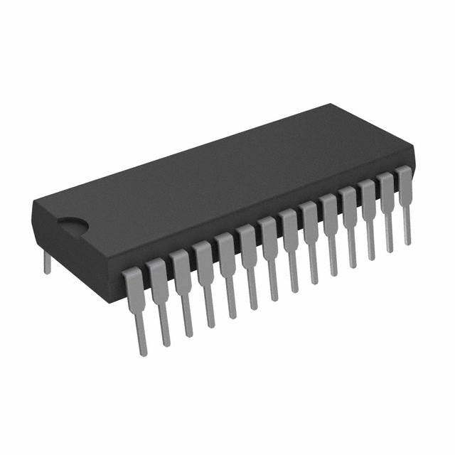
ICGOO在线商城 > AS3611-BDFM-A
- 型号: AS3611-BDFM-A
- 制造商: AUSTRIAMICROSYSTEMS
- 库位|库存: xxxx|xxxx
- 要求:
| 数量阶梯 | 香港交货 | 国内含税 |
| +xxxx | $xxxx | ¥xxxx |
查看当月历史价格
查看今年历史价格
AS3611-BDFM-A产品简介:
ICGOO电子元器件商城为您提供AS3611-BDFM-A由AUSTRIAMICROSYSTEMS设计生产,在icgoo商城现货销售,并且可以通过原厂、代理商等渠道进行代购。 提供AS3611-BDFM-A价格参考以及AUSTRIAMICROSYSTEMSAS3611-BDFM-A封装/规格参数等产品信息。 你可以下载AS3611-BDFM-A参考资料、Datasheet数据手册功能说明书, 资料中有AS3611-BDFM-A详细功能的应用电路图电压和使用方法及教程。
| 参数 | 数值 |
| 产品目录 | 集成电路 (IC) |
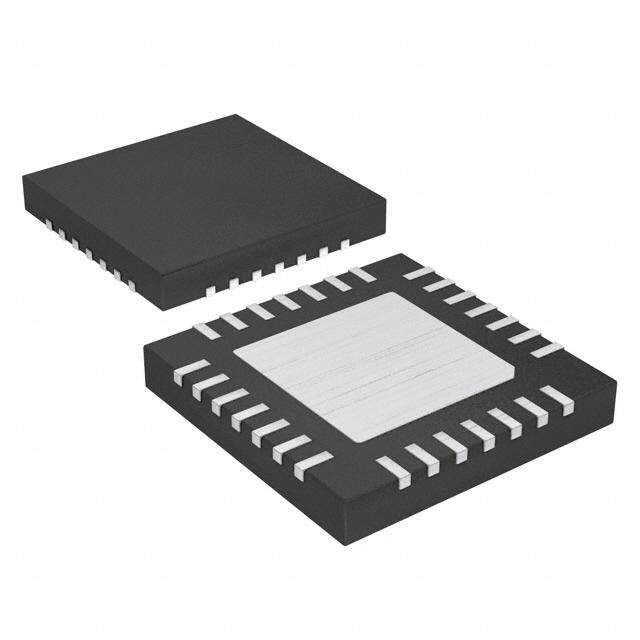
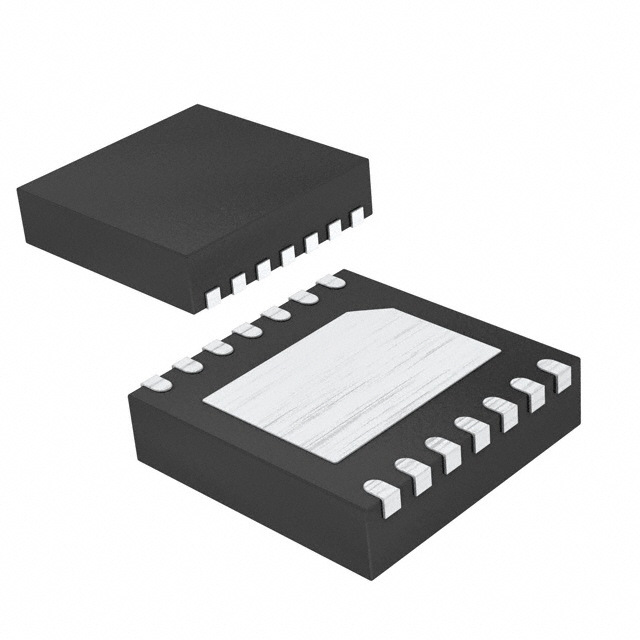
| 描述 | IC CHARGER STEP-DOWN 14-MLP |
| 产品分类 | |
| 品牌 | ams |
| 数据手册 | |
| 产品图片 | |
| 产品型号 | AS3611-BDFM-A |
| rohs | 无铅 / 符合限制有害物质指令(RoHS)规范要求 |
| 产品系列 | * |
| 供应商器件封装 | 14-MLPD(3x3) |
| 其它名称 | AS3611-BDFM-ACT |
| 功能 | 充电管理 |
| 包装 | Digi-Reel® |
| 安装类型 | 表面贴装 |
| 封装/外壳 | 14-WFDFN 裸露焊盘 |
| 工作温度 | -40°C ~ 85°C |
| 标准包装 | 1 |
| 电压-电源 | 2.7 V ~ 5.5 V |
| 电池化学 | 锂离子,锂聚合物,磷酸铁锂 |


- 商务部:美国ITC正式对集成电路等产品启动337调查
- 曝三星4nm工艺存在良率问题 高通将骁龙8 Gen1或转产台积电
- 太阳诱电将投资9.5亿元在常州建新厂生产MLCC 预计2023年完工
- 英特尔发布欧洲新工厂建设计划 深化IDM 2.0 战略
- 台积电先进制程称霸业界 有大客户加持明年业绩稳了
- 达到5530亿美元!SIA预计今年全球半导体销售额将创下新高
- 英特尔拟将自动驾驶子公司Mobileye上市 估值或超500亿美元
- 三星加码芯片和SET,合并消费电子和移动部门,撤换高东真等 CEO
- 三星电子宣布重大人事变动 还合并消费电子和移动部门
- 海关总署:前11个月进口集成电路产品价值2.52万亿元 增长14.8%


PDF Datasheet 数据手册内容提取
austriamicrosystems AG is now ams AG The technical content of this austriamicrosystems datasheet is still valid. Contact information: Headquarters: ams AG Tobelbaderstrasse 30 8141 Unterpremstaetten, Austria Tel: +43 (0) 3136 500 0 e-Mail: ams_sales@ams.com Please visit our website at www.ams.com
Datasheet AS3610/11 Switching Charger for Li-Ion/LiPo/LiFePO4 powered devices 1 General Description 2 Key Features d The AS3610/11 is a highly integrated standalone or optional I²C (cid:1) DCDC USB Charger controlled step down charger. All supervision and regulation (cid:1) 1.25A, 3MHz DCDC Charger i functions are realized internal and independent from the processor. l (cid:1) OTG Boost with low IQ (700µA) up to 500mA The 100/500mA USB current limit can be set via a dedicated control a pin. Other limits like 900mA can be programmed in the OTP ROM. (cid:1) 22V over voltage protection v In addition, the Charger can generate a 5.05V output supply at (cid:1) Seamless 100% Mode VBUS for USB OTG. (cid:1) Reverse Polarity protection on VBUS AS3610 features an I2C interface which can be used by a micro- l (cid:1) NTC support controller to fully control all functionality of the chip. Charging current l and EOC current can be set with external resistors and adjusted via (cid:1) Low side LED driver i register settings if needed. (cid:1) No eGxternal shunt resistor requiredt AS3611 is a stand-alone version of this charger IC. Charging and (cid:1) “No Battery” operation withouts voltage drop EOC current is set by resistor only. Functions like OTG boost mode or max current limit for wall adapter mode can be enabled using A(cid:1) Package: MLPD14 3x3m m dedicated pins. t n 3 Application s e The device is ideal as 1 Cell LiIon, LiPo or LiFePO4 charger for m Figure 1. AS3610/11 Block Diagram mobile phones and portable devices. t n a o c l a c i n h c e T www.austriamicrosystems.com/Battery-Chargers/AS3610 1.01 1 - 25
AS3610/11 Datasheet - Contents Contents 1 General Description ..................................................................................................................................................................1 2 Key Features ............................................................................................................................................................................1 3 Application ................................................................................................................................................................................1 4 Pin Assignments .......................................................................................................................................................................3 d 4.1 Pin Descriptions ...................................................................................................................................................................................3 i 5 Absolute Maximum Ratings ......................................................................................................................................................4 l 6 Electrical Characteristics .........................................................................................................................................................a.5 7 Typical Operating Characteristics .............................................................................................................................................7 v 8 Detailed Description .................................................................................................................................................................9 8.1 Charge Controller .......................................................................................................................................................... .......................9 l 8.2 Step up converter mode (OTG Boost) ...............................................................................................................................................12 l 8.3 2-Wire-Serial Control Interface ....................................................................... ...............................................i.....................................12 8.4 AS3611 pre-programmed variants ............................................................G..............................................t...........................................14 8.5 Register Description ..........................................................................................................................s.................................................15 8.6 Register Overview ..............................................................................................................................................................................19 A 9 Application Information ...........................................................................................................................................................21 t 10 Package Drawings and Markings ................................ ..........................................n...............................................................22 11 Ordering Information ................................................s.............................................................................................................24 e m t n a o c l a c i n h c e T www.austriamicrosystems.com/Battery-Chargers/AS3610 1.01 2 - 25
AS3610/11 Datasheet - Pin Assignments 4 Pin Assignments Figure 2. AS3610/11 Pin Assignments (Top View) d i l a v l l i G t s 4.1 Pin Descriptions A Table 1. Pin Descriptions t Pin Name Pin Name n Pin Number Pin Types Supply Description AS3610 AS3611 e 1 XEN XEN m VBAT XEnable pin for step down charger I tSet current limit in charger mode. 100mA / 500mA 2 USB500 USB500 nVBAT USB current limit. a 3 NTC NTC VDD_INT NTC input o 4 VBAT VBAT Analog pin Analog Sense input 5 VDD_INT VDD_INT c Connect 1µF (0402) for internal LDO supply 2.5V SW node of step down charger. Connect to 1µH 6 SW SW inductor (chip coil) l 7 VBUS VBUS aPower pin Charger input (USB voltage or charger voltage) 8 PGND PGND Power GND connection of step down charger c Digital Open Drain Output 9 STAT STAT Pulled to GND for error / status indication via LED i pin n 10 I_TERM I_TERM VBAT Sets trickle / EOC current 11 I_SET h I_SET Analog pin VBAT Sets charging current (Constant current) 12 VSS VSS Analog VSS c Digital Open Drain Output SCL pin; Requires an external VBAT I²C clock line 13 e pull-up resistor T OTG_BOOST I VBAT switches mode to OTG boost Digital Open Drain Output SDA pin; Requires an external VBAT I²C data line pull-up resistor 14 selects the highest input current limit for wall adapter CHG_DET I VBAT charging www.austriamicrosystems.com/Battery-Chargers/AS3610 1.01 3 - 25
AS3610/11 Datasheet - Absolute Maximum Ratings 5 Absolute Maximum Ratings Stresses beyond those listed in Table 2 may cause permanent damage to the device. These are stress ratings only, and functional operation of the device at these or any other conditions beyond those indicated in Operating Conditions on page 5 is not implied. Exposure to absolute maximum rating conditions for extended periods may affect device reliability. Table 2. Absolute Maximum Ratings d Symbol Parameter Min Max Unit Comments i Electrical Parameters l V_HV20 High voltage pins -2 22 V Applicable to high voltage pins: VBUS, SW, STATa Applicable to 5V-pins: VBAT, XEN, SDA, SCL, V_MV 5V pins -0.3 7.0 V USB500, I_SET, I_TERM v V_LV 3.3V pins -0.3 5.0 V Applicable to 3.3V-Pins: VDD_INT, NTC IIN Input pin current -100 +100 mA Norm: JEDEC JESDl78 l Electrostatic Discharge i VESD Electrostatic discharge +/-15001 V G Norm: JEDECt JESD22-A114F s Temperature Ranges and Storage Conditions SCSB Operating Temperature -40 +85 A ºC t TJ Junction Temperature +110 ºC n Storage Temperature Range -55 s+150 ºC Humidity non-condensing 5 85 % e m Temperature (soldering) t n 2 Norm IPC/JEDEC J-STD-020 TBODY Package Body Temperaturae 260 ºC The lead finish for Pb-free leaded packages is matte tin o (100% Sn) Moisture Sensitive Level 3 Represents a max. floor life time of 168h c 1. pin STAT is +/-750V only 2. The reflow peak soldering temperature (body temperature) is specified according IPC/JEDEC J-STD-020 “Moisture/Reflow Sensitivity l Classification for Nonhermetic Solid State Surface Mount Devices” a c i n h c e T www.austriamicrosystems.com/Battery-Chargers/AS3610 1.01 4 - 25
AS3610/11 Datasheet - Electrical Characteristics 6 Electrical Characteristics VBAT=+2.7V...+5.5V, TA =-40ºC...+85ºC. Typical values are at VBAT=+3.6V, TA=+25ºC, unless otherwise specified. The parameters with min and max values are guaranteed with production tests or SQC (Statistical Quality Control) methods. Table 3. Operating Conditions d Symbol Parameter Notes Min Typ Max Unit Operating Range i VHV20 High voltage pins Applicable to high voltage pins: VBUS, SW. -2 5.0 20 V l a Applicable to 5V pins: VBAT, XEN, SDA, VMV 5V pins SCL, USB500, I_SET, I_TERM -0.3 5.5 V v VLV 3.3V pins Applicable to 3.3V-Pins: VDD_INT, NTC -0.3 3.6 V TAMB Ambient Temperature -40 25 l85 deg Operating Currents l i IVBUS_ACT if step dVoBwUnS c hcaurrgreenr ti,s active IIUUSSBB lliimmiitt >< 110000GmmAA st150 mmAA VBAT current, IBOOST if boost active without load VABAT=4.2V 700 µA t IVBUS_OFF VBUS current in OFF mode VBUS=5V, TJ < 85ºC n 16 µA IVBAT VBAT quiescent current in OFF mode InscludVinBgA leTa=k4a.2gVe, cTuJr <re 8n5t ºteoC VBUS 16 µA m Charging Mode Parameter t Step Down charger disabled below this VBUS_UVLO VBUS undervoltage lockout threshold. -15n0mV hysteresis 3.7 3.8 3.9 V a Step Down charger disabled above this VBUS_OV VBUS overvoltage off mode threshoold. -140mV hysteresis 6.3 6.5 6.7 V c 3.9 VBUS minimum voltage to regulate Vnom - 4.2 Vnom+ VBUS_min current to VBAT Programmable (2-bit) 0.12 4.5 0.12 V 4.7 l Charge current accuracy of maean Current selected by resistor on ISET pin: 550… ICHARGE output current ICHARGE = 21450/RSET and register -8% 1250 +8% mA const_curr<1:0> c ITERM Termination ancdu rtirreicnktle (precharge) Current seIlTeEcRteMd =b y1 2re0s0i/sRtoTrE RonM ITERM pin: -4-03m0A% or 5200…0 +4+03m0A% or mA n 100mA USB current limit 88 93 105 mA IUSB USBh input current limit resistor 500mA USB current limit 450 475 500 mA 900mA USB current limit 800 850 900 mA c VSOFT Apply ISOFT cuvrroeltnatg beelow this VBAT Hysteresis -100mV 1.9 2.0 2.1 V e ISOFT Soft current, if VBAT is below VSOFT 25 38 55 mA T VTRICKLE Apply trictkhleis cVuBrrAeTn tv (o=ltITaEgReM ) below -0.1 2.9 +0.1 V 3.5...4. VCHARGE End of charge voltage 20mV steps Programmable 44 End of charge accuracy 4.2V EOC voltage, -40..85°C -1 +1 % VCHDET Charge detect voltage difference VBUS-VBAT +1 +40 +100 mV www.austriamicrosystems.com/Battery-Chargers/AS3610 1.01 5 - 25
AS3610/11 Datasheet - Electrical Characteristics Table 3. Operating Conditions Symbol Parameter Notes Min Typ Max Unit VRESUME Resume voltage VTHRESHOLD = VCHARGE - VRESUME 120 mV RPMOS Resistance of PMOS switch 300 mW RNMOS Resistance of NMOS switch 300 mW d fOSC Switching frequency 2.7 3.0 3.3 MHz i DMAX Maximum duty cycle Smooth transition. No skipmode. 100 % l a Minimum ON time of PMOS. Below this TMIN Minimum ON time of PMOS value, transition to pulseskip mode 60 nsec v ICOIL Coil current limit 1.7 A Boost Mode Parameter l VBUS regulated voltage in boost VBOOST mode 4.9 5.05l5.2 V i IBOOST Boost current 2.7<VBAT<4.5 (boost_Glowcurr=1) 200 t mA IHBOOST Boost current (high current mode) 3.2<VBAT<4.5 (boost_lowcurr=0) 500s mA ICOIL Coil current limit A 01..755 A t ISU Stepup no load current on VBAT VBAT=4.2V n 700 m A Thermal Limitation s e Thermal current regulation for charger TREG mode m 110 °C t TSHDOWN Thermal shutdown limit n 140 °C NTC Charging Temperature Range a o Battery Temperature high level 500 or VBATTEMP_ON (50 or 55 ºC) NTCbeta = 4200 ntc_temp=0 400 mV c Battery Temperature low level 600 or VBATTEMP_OFF (45 or 50 ºC) NTCbeta = 4200 ntc_temp=1 500 mV IBATTEMP NTC Bias Current l 100kW NTC -14% 15 +14% µA a IBATTEMP NTC Bias Current 10kW NTC -10% 150 +10% µA IO characteristics c SCL/CHG_DET, SDA/OTG_BOOST, VIL USB50i0, XEN -0.3 0.4 V Low Levnel input voltage SCL/CHG_DET, SDA/OTG_BOOST, h VIH USB500, XEN 1.4 VBAT V High Level input voltage c e T www.austriamicrosystems.com/Battery-Chargers/AS3610 1.01 6 - 25
AS3610/11 Datasheet - Typical Operating Characteristics 7 Typical Operating Characteristics CVBAT=10µF, CVBUS=10µF, L=1µH, Figure 3. USB Current (100mA limit) Figure 4. USB Current (500mA limit) d USB current (100mA limit) USB current (500mA limit) 0,12 0,6 i l 0,1 0,5 a 0,08 0,4 v IUSB [A]0,06 IUSB [A]0,3 l 0,04 0,2 l i 0,02 VUSB=4.5V, Iusb=100mA 0,1 G VUtSB=4.5V, Iusb=500mA VUSB=5.5V, Iusb=100mA VUSB=5.5V, Iusb=500mA VUSB=6.5V, Iusb=100mA sVUSB=6.5V, Iusb=500mA 0 0 2,5 2,7 2,9 3,1 3,3 3,5 3,7 3,9 4,1 4,3 A2,5 2,7 2,9 3,1 3,3 3,5 3,7 3,9 4,1 4,3 VBAT [V] tVBAT [V] Figure 5. Current into Battery (100mA limit) Figure 6. Current into Bnattery (500mA limit) s Battery current (100mA IUSB limit) eBattery current (500mA IUSB limit) 0,3 m 0,9 0,8 t 0,25 n 0,7 a 0,2 o0,6 IBAT [A]0,15 c IBAT [A]00,,45 0,1 0,3 l 0,2 0,05 VUSB=4.5V, Iusab=100mA VUSB=4.5V, Iusb=500mA VUSB=5.5V, Iusb=100mA VUSB=5.5V, Iusb=500mA 0,1 VUSB=6.5V, Iusb=100mA VUSB=6.5V, Iusb=500mA c 0 0 2,5 2,7 2,9 3,1 3,3 3,5 3,7 3,9 4,1 4,3 2,5 2,7 2,9 3,1 3,3 3,5 3,7 3,9 4,1 4,3 VBAiT [V] VBAT [V] n h c e T www.austriamicrosystems.com/Battery-Chargers/AS3610 1.01 7 - 25
AS3610/11 Datasheet - Typical Operating Characteristics Figure 7. Charging Cycle 1 Figure 8. Charging Cycle 2 Battery current (54mA prechg, 550mA CC) Battery current (100mA prechg, 1200mA CC) 0,7 1,4 0,6 1,2 d 0,5 1 IBAT [A]00,,34 IBAT [A] 00,,68 ali 0,2 0,4 v VUSB=4.5V, 54/550mA VUSB=4.5V, 100/1192mA 0,1 VUSB=5.5V, 54/550mA 0,2 VUSB=5.5V, 100/1192m A VUSB=6.5V, 54/550mA VUSB=6.5V, 100/1192mA l 0 0 2,5 2,7 2,9 3,1 3,3 3,5 3,7 3,9 4,1 4,3 2,5 2,7 2,9 3,1 3,3 3,5 3,7l3,9 4,1 4,3 VBAT [V] VBAT [V] i G t s Figure 9. Efficiency @550mA Figure 10. Efficiency @1.2A A DCDC Charger Efficiency @ Charge Current=550mA DCDC Charger Effticiency @ Charge Current=1.2A 100 100 n s 95 95 e 90 m 90 t 85 85 %] %] n Efficiency [ 7850 a oEfficiency [ 7850 70 c 70 VUSB=4.5V, 54/550mA VUSB=4.5V, 100/1192mA 65 VUSB=5.5V, 54/550mA 65 VUSB=5.5V, 100/1192mA VUSB=6.5V, 54/550mA VUSB=6.5V, 100/1192mA l 60 60 3 3,2 3,4 3,6 3,8 a4 4,2 4,4 3 3,2 3,4 3,6 3,8 4 4,2 4,4 VBAT [V] VBAT [V] c i Figure 11. Boost Efficiency Figure 12. Booster Output Voltage n BOOST Efficiency VUSB voltage regulation 100 h 5,1 VBAT=2.7V, boost_lowcurr=0 5,08 95 VBAT=3.2V, boost_lowcurr=0 c 5,06 VBAT=4.0V, boost_lowcurr=0 90 5,04 e 85 %] 5,02 Efficiency [ 80T VUSB [A]4,985 75 4,96 70 4,94 65 VBAT=4.0V, boost_lowcurr=1 4,92 60 4,9 0 0,05 0,1 0,15 0,2 0,25 0,3 0,35 0,4 0 0,1 0,2 0,3 0,4 0,5 0,6 0,7 0,8 IBUS [V] IUSB [V] www.austriamicrosystems.com/Battery-Chargers/AS3610 1.01 8 - 25
AS3610/11 Datasheet - Detailed Description 8 Detailed Description 8.1 Charge Controller 8.1.1 General Description The AS3610/11 device serves as a standalone battery charge controller supporting rechargeable Lithium Ion (Li+) batteries. Requiring only a few d external components, a full-featured battery charger with a high degree of flexibility can easily be realized. The main features of the controller are: i (cid:1) Charge adapter detection l a (cid:1) Internal voltage regulator (cid:1) Low current (soft) charging v (cid:1) Low current (trickle) charging (cid:1) Constant current charging l (cid:1) Constant voltage charging l i (cid:1) 22V input overvoltage protection G t (cid:1) Battery presence indication s (cid:1) Operation without battery A (cid:1) Input current limitation t (cid:1) Input voltage drop regulation n s Figure 13. Detailed Block Diagram e m t n a o c l a c i n h c e T www.austriamicrosystems.com/Battery-Chargers/AS3610 1.01 9 - 25
AS3610/11 Datasheet - Detailed Description Figure 14. Detailed Block Diagram d i l a v l l i G t s A t n s 8.1.2 Charging Cycle Description e m 8.1.2.1 Charge adapter detection t The charger uses an integrated detection circuit to determine if an external chanrge adapter has been applied to the VBUS pin. If the VBUS voltage exceeds the battery voltage at pin VBUaS by VCHDET the ChDet bit in the ChargerStatus1 register will be set. That detection de-bounce time is approx. 300msec for rising ChDet and approx. 30msec for fallingo ChDet signal (debounce_timer=00b). 8.1.2.2 Low current soft charging c When the charger is detected and enabled (chg_en=1), no stop charging condition is active and the battery voltage is below VSOFT, the charging cycle is started with soft_charging. In that mode the charg er is acting as a linear charger down to VBAT. With a current of ISOFT l 8.1.2.3 (Trickle) Pre-charging a If the battery voltage exceeds VSOFT, but is below VTRICKLE, and the bit prechg_en is set, the trickle charging is started. c In that mode the charging current is defined by the external resistor on pin I_TERM or the input current limit if e.g. 100mA input current limit is active. i n 8.1.2.4 Constant current charging If the battery voltage is above VTRICKLE and below VEOC (or above VSOFT if prechg_en=0) the charging current is defined by the resistor on pin h I_SET. In addition the current can be reduced by I2C with the register setting of constcurr. (AS3610 only) 8.1.2.5 Constanct voltage charging Constant voltage charge mode is initiated, if the battery voltage has reached the VEOC threshold. e The charge current is monitored during constant voltage charging. It will be decreasing from its initial value during constant current charging and eventuTally drop below the value set by the resistor on pin I_TERM. If the measured charge current is less than or equal to ITERM, the charging cycle is terminated and EOC is set. The termination current may be reduce by a factor of 2 by setting the eoccurr bit to 1. www.austriamicrosystems.com/Battery-Chargers/AS3610 1.01 10 - 25
AS3610/11 Datasheet - Detailed Description 8.1.3 Charger States d i l a v l l i G t s A t n s e 8.1.4 Stop charging conditions m There are multiple safety features implemented that trigger a stop_charging condittion: n These are the following: a - Battery temperature too high. If ntc_on=1 and voltage at pin NTCo is below VBATTEMP - Timeout timer expired (If ch_timeout>0 and charging time has been exceeded). Can be reset by unplugging the charger, setting chg_en=0 or writing charging_tmax=0 c - VBUS_OV exceeded - VBUS_UVLO reached - Die temp>140deg (ov_temp_140 set) l a 8.1.5 Battery presence indication and operation without battery c After EOC state is reached a timer for NOBAT detection is started. If there is no battery present, the voltage will drop to VNOBAT_REG. Depending on the load on VBAT and the capacitor on VBAT this might take some milliseconds to 1 second. The charger will restart charging i (ConstantCurrent charging) after 100msec. n The 100msec dead time is necessary to get a battery oscillation frequency of below 10Hz, if there is no battery present and NTC battery detection is not enabled. h If No_bat_det=1 and the NOBAT detection timer is below 2 seconds after reaching EOC state, and this happens 2 times in serial, the state “operation without bcattery” is entered. If the nobat_ntc_det bit is set the looping described above will be stopped and a NTC detection is started. e A pull up current of 0.5uA is applied to NTC. If the NTC voltage is above 1.8V, the state machine stays in the no bat state. If the BATTEMP voltage is below 1.8V, a charging cycle is restarted. T 8.1.6 VBUS undervoltage regulation If the voltage on VBUS drops below Vchg_min the current is regulated down to avoid overloading of the input source. 8.1.7 Charger overvoltage protection This blocks checks if the charger voltage VBUS is above VBUS_OV. In that case the bit stop_charging is set and the charging is stopped until VBUS is below VBUS_OV. www.austriamicrosystems.com/Battery-Chargers/AS3610 1.01 11 - 25
AS3610/11 Datasheet - Detailed Description 8.1.8 NTC supervision This charger block also features a supply for an external NTC resistor to measure the battery temperature while charging. If the temperature is too high (voltage on NTC pin is below VBATTEMP_ON) the charger will stop operation (stop_charging=1). When the battery temperature drops, the voltage on NTC pin will rise above VBATTEMP_OFF and the charger will start charging again. This is forming a temperature hysteresis of about 3 to 5°C to avoid an oscillation of the charger. The levels for switching off the charger (ntc_temp: 45ºC or 55ºC) as well as the type of NTC (ntc_10k: 10k or 100k) can be selected via d register settings. The battery temperature supervision via the NTC can be switched off (ntc_on = 0). The supply for the NTC will be only on when a charger is detected and ntc_on bit is set. i l 8.2 Step up converter mode (OTG Boost) a The step down charger can also be used in a boost mode providing an output voltage VBOOST on pin VBUS typ 5.05V. In that mode the vcurrent direction is inverted to the charging mode providing current from the battery to the VBUS pin. To enable that mode, it’s necessary that the charger is disabled (XEN=1 or chg_en=0) and the bit boost_en is set (and for AS3611 the pin OTG_BOOST=1). The bit boost_lowcurr se lects the output current capability between 200mA and 500mA. l l 8.2.1 Softstart of OTG booster i There is a softstart implemented to reduced inrush current on the V inputG. For approx. 1msec after tthe booster is enabled the BAT s output current is limited below 100mA. After that startup time the full current is available. A 8.2.2 Short-circuit and overvoltage protection circuit t To protect the booster, the battery capacity and the circuit connected to VBUS there are multiple protection circuits implemented: n - VBAT drops below 2.6V (typ) s - VBUS is above 5.3V (typ) e - Booster is in current limit operation (e.g. output VBmUS is overloaded or shorted to GND) If one of these conditions is valid for more that 30msec debounce time (debounce_ttimer=00b), the booster is stopped and the boost_error bit is set. To restart the booster it’s necessary to set boost_en=0 and 1 again. (For AnS3611 the OTG_BOOST pin has to be set to 0 and 1 again). a If the die Temp is above 140deg the booster is stopped and restarted automatically when the die temperature drops. o 8.3 2-Wire-Serial Control Interface c 8.3.1 Feature List (cid:1) Fast-mode capability (max. SCL-frequency is 400 kHz) l (cid:1) 7+1-bit addressing mode a (cid:1) 60h x 8-bit data registers (word address 0x00 - 0x60) c (cid:1) Write formats: Single-Byte-Write, Page-Write (cid:1) Read formats: Current-Address-iRead, Random-Read, Sequential-Read n (cid:1) SDA input delay and SCL spike filtering by integrated RC-components h 8.3.2 Protocol Table 4. 2-Wire Serial Symbol Definition c Symbol Definition RW Note e S Start condition after stop R 1 bit T Sr Repeated start R 1 bit DW Device address for write R 1000 1100b (8Ch) DR Device address for read R 1000 1101b (8Dh) WA Word address R 8 bit A Acknowledge W 1 bit N No Acknowledge R 1 bit www.austriamicrosystems.com/Battery-Chargers/AS3610 1.01 12 - 25
AS3610/11 Datasheet - Detailed Description Table 4. 2-Wire Serial Symbol Definition Symbol Definition RW Note reg_data Register data/write R 8 bit data (n) Register data/read W 8 bit P Stop condition R 1 bit d WA++ Increment word address internally R during acknowledge i Figure 15. Byte Write l a S DW A WA A reg_data A P v write register WA++ l l Figure 16. Page Write i G t s S DW A WA A reg_data 1 A reg_data 2 A ... reg_data n A P A write register write register t write register WA++ WA++ WA++ n s Byte Write and Page Write formats are used to write data to the slave. e The transmission begins with the START condition, whichm is generated by the master when the bus is in IDLE state (the bus is free). The device- write address is followed by the word address. After the word address any numbert of data bytes can be sent to the slave. The word address is incremented internally, in order to write subsequent data bytes on subsequent address locations. n For reading data from the slave device, the maaster has to change the transfer direction. This can be done either with a repeated START condition followed by the device-read address, or simply with a new transmissiono START followed by the device-read address, when the bus is in IDLE state. The device-read address is always followed by the 1st register byte transmitted from the slave. In Read Mode any number of subsequent register bytes can be read from the slave. The word address is incremented internally. c Figure 17. Random Read l a S DW A WA A Sr DR A data N P c read register WA++ i Random Read and Sequential Renad are combined formats. The repeated START condition is used to change the direction after the data transfer from the master. The word address transferh is initiated with a START condition issued by the master while the bus is idle. The START condition is followed by the device-write address and the word address. c In order to change the data direction a repeated START condition is issued on the 1st SCL pulse after the acknowledge bit of the word address transfer. After the reception of the device-read address, the slave becomes the transmitter. In this state the slave transmits register data located e by the previous received word address vector. The master responds to the data byte with a not-acknowledge, and issues a STOP condition on the bus. T Figure 18. Sequential Read S DW A WA A Sr DR A data A reg_data 2 A ... reg_data n N P read register read register read register WA++ WA++ WA++ www.austriamicrosystems.com/Battery-Chargers/AS3610 1.01 13 - 25
AS3610/11 Datasheet - Detailed Description Sequential Read is the extended form of Random Read, as more than one register-data bytes are transferred subsequently. In difference to the Random Read, for a sequential read the transferred register-data bytes are responded by an acknowledge from the master. The number of data bytes transferred in one sequence is unlimited (consider the behavior of the word-address counter). To terminate the transmission the master has to send a not-acknowledge following the last data byte and generate the STOP condition subsequently. Figure 19. Current Address Read d S DR A data A reg_data 2 A ... reg_data n N P i read register read register read register l WA++ WA++ WA++ a v To keep the access time as small as possible, this format allows a read access without the word address transfer in advance to the data transfer. The bus is idle and the master issues a START condition followed by the Device-Read address. Analogous to Random Read, a single byte transfer is terminated with a not-acknowledge after the 1st register byte. Analogous to Sequential Read an unlimited number of data bytes can l be transferred, where the data bytes has to be responded with an acknowledge from the master. For termination of the transmission the master l sends a not-acknowledge following the last data byte and a subsequent STOP condition. i The AS3610 is compatible to the NXP two wire specification http://www.nxp.com/acroGbat_download2/literature/939t8/39340011.pdf Version 2.1 January 2000 for standard and fast mode (no high speed mode). s 8.4 AS3611 pre-programmed variants A AS3611 is intended to work stand-alone with out an micro-controller. For this use case some of the btasic configurations have to be pre- programmed into the device. Two basic configurations are shown in the tables below. Adaptationns to these configurations are possible upon request. s Table 5. AS3611-A stand alone version for Li-Ion/LiPo,100kOhm NTC e m Reg. Addr. Value Description t Reg. Name 0 7Fh standalone mode=1, Boost_en=1, prechg_en=1, nnobat_det=0 Charger Control a 1 63h Veoc=4.2V, Vchg_min=4.2 Charger Voltage Control o 2 00h Charger Current Control 3 05h 100kOhm NTC, low_temp range (45/50°C) NTC Supervision c ch_timeout=5h, stat_mode: charging=on; EOC=1Hz blinking, stop_charging 4 8Ah Charger supervision or boost_error=5Hz l Table 6. AS3611-B stand alone version for Li-Ion/LiPo,10kOhm NTC a Reg. Addr. Value Description Reg. Name c 0 7Fh standalone mode=1, Boost_en=1, prechg_en=1, nobat_det=0 Charger Control 1 63h Veoc=4i.2V, Vchg_min=4.2 Charger Voltage Control 2 00h n Charger Current Control 3 07h 10kOhm NTC, low_temp range (45/50°C) NTC Supervision h ch_timeout=5h, stat_mode: charging=on; EOC=1Hz blinking, stop_charging 4 8Ah Charger supervision or boost_error=5Hz c Table 7. AS3611-C stand alone version for FePO4, 10kOhm NTC e Reg. Addr. Value Description Reg. Name T0 7Fh standalone mode=1, Boost_en=1, prechg_en=1, nobat_det=0 Charger Control 1 47h Veoc=3.64V, Vchg_min=4.2 Charger Voltage Control 2 01h eoccurr=1 Charger Current Control 3 05h 100kOhm NTC, low_temp range (45/50°C) NTC Supervision ch_timeout=3h, stat_mode: ch_det=on; EOC=1Hz blinking, stop_charging 4 A6h Charger supervision or boost_error=5Hz www.austriamicrosystems.com/Battery-Chargers/AS3610 1.01 14 - 25
AS3610/11 Datasheet - Detailed Description 8.5 Register Description Charger Control Register (Address 0). Charger Control Addr: 0 This register controls the mode of the charger and the charger state machine. d Bit Bit Name Default Access Bit Description ON/OFF control of USB charger input i 0 Chg_en 1b/ROM R/W 0 Charger disabled l 1 Charger enabled, if XEN=0 a ON/OFF control of Step up for USB OTG v Normal operation (usb current=0..6): 0 Step up disabled 1 Step up enabled l 1 Boost_en 0b/ROM R/W l AS3611 standalone charger operation only w/o I²C (usb current=7) i 0 StepG up disabled t 1 Step up enabled, if OTG_BOsOST=1, Step up disabled, if OTG_BOOST=0 USBA input current limit, AS3610 I²C version only t 000b 100mA, if pin USB500=0 500mA, if pin UnSB500=1 s 001b 100mA e 010b 500mA limit m 011b 900mA limit 4:2 usb_current 000b/ROM R/W 100b utnlimited 101bnNA a 110b unlimited o111b AS3611 stand alone charger only w/o I²C CHG_DET=1 and USB500=0 fi 100mA limit c CHG_DET=1 and USB500=1 fi 500mA limit CHG_DET=0 and USB500=1 fi unlimited current 0 Pre-charge (trickle charge) disabled. Charger starts with l constant current, if VBAT>2.0V (current set by resistor I_SET) 5 prechg_en 1b/ROM a R/W 1 Pre-charge (trickle charge) enabled. Charger starts with trickle current, if 2.9V>VBAT>2.0V (Current set by resistor c I_term) 0 Off time of step down charger enabled. If 100% pmos on i mode is needed, off pulses are skipped n 6 disable_toff 1b/ROM R/W 1 Off time of step down charger disabled. Smooth transition h to 100% pmos on if needed (VBUS-VBAT is small) 0 Nobat detection disabled. c 7 No_bat_det 1b/ROM R/W 1 Nobat detection enabled. If No Battery is detected a small current through NTC (approx. 0.5µA), checks if a battery e is connected again. A NTC is necessary for that setting. T www.austriamicrosystems.com/Battery-Chargers/AS3610 1.01 15 - 25
AS3610/11 Datasheet - Detailed Description Charger Voltage Control Register (Address 1). Charger Voltage Control Addr: 1 This register controls the charger voltages. Bit Bit Name Default Access Bit Description End of charge voltage on VBAT d 0 3.5V 100011b/ ... ... i 5:0 Veoc R/W ROM 35 4.2V l ... ... a 47 4.44V v Minimum charger (VBUS) voltage. Current is regulated down, if VBUS voltage drops below this level: 7:6 Vchg_min 00b/ROM R/W 0 VBAT < 3.9V l 1 VBAT < 4.2V l 2 VBAT < 4.5V i 3 VBAGT < 4.7V t s Charger Current Control Register (Address 2). A Charger Current Control t Addr: 2 This register controls the ch arger currents. n s Bit Bit Name Default Access Bit Description e m Current ratio selection between trickle and EOC current 0b/ (defined byt resistor RTERM) 0 eoccurr ROM R/W 0 nEOC current = ITERM, Trickle current = ITERM a 1 EOC current = ITERM / 2, Trickle current = ITERM o ConstantCurrent setting c 0 Constant Current = ICHARGE 2:1 constcurr 00b/ROM R/W 1 Constant Current = 0.81*ICHARGE 2 Constant Current = 0.60*ICHARGE l 3 Constant Current = 0.40*ICHARGE a Current selection for boost mode 3 boost_lowcurr 0b/cROM R/W 0 500mA maximum current 1 200mA maximum current i 4 NA NA NA NA n Enables 100% on mode of PMOS 5 en_pohn 0b/ROM R/W 0 100% mode disabled (smooth 100% mode, if disable_toff=1) c 1 100% mode enabled. Select debounce timer e 0 30msec debounce timer for comparator output 7:6 deb_timer 00b/ROM R/W 1 3msec debounce timer T 2 NA 3 NA www.austriamicrosystems.com/Battery-Chargers/AS3610 1.01 16 - 25
AS3610/11 Datasheet - Detailed Description NTC Supervision Register (Address 03). NTC Supervision Addr: 03 These bits define the battery temperature supervision. Bit Bit Name Default Access Bit Description ON/OFF control of battery NTC supervision d 0 ntc_on 1b/ROM R/W 0 Disabled 1 Enabled i l Select NTC resistor type a 1 ntc_10k 1b/ROM R/W 0 100kW 1 10kW v Select NTC temperature shutdown 2 ntc_temp 1b/ROM R/W 0 high temperature range (50 or 55 ºC) l 1 low temperature range (45 or 50 ºC) l i Charger Supervision Register (Address 04). G t s Charger Supervision Addr: 04 A These bits define charging timer settings. t Bit Bit Name Default Access Bit Description n s Charging timeout timer 0 Chargineg timer disabled m 1 0.5 hour 2 1t hour 3 n1.5 hour a 4 2 hour o5 2.5 hour 6 3 hour 3:0 ch_timeout 1010b/ROM R/W 7 3.5 hour c 8 4 hour 9 4.5 hour l 10 5 hour a 11 5.5 hour 12 6 hour c 13 6.5 hour 14 7 hour i 15 7.5 hour n 0 Read: no timeout reached 4 charging_tmax 0b/ROM R/W Write: reset charger timeout counter h 1 tCHARGING,MAX timeout reached and charging stopped Function of Status pin: c 0 always off 1 ch_det=ON e 2 ch_det=ON, stop_charging or boost_error=5Hz blinking 7:T5 stat_mode 010b/ROM R/W 3 Charging=ON, stop_charging or boost_error=5Hz blinking 4 Charging=ON, EOC=1Hz blinking, stop_charging or boost_error=5Hz blinking 5 ch_det =ON, EOC=1Hz blinking, stop_charging or boost_error=5Hz blinking www.austriamicrosystems.com/Battery-Chargers/AS3610 1.01 17 - 25
AS3610/11 Datasheet - Detailed Description Charger Status1 Register (Address 05). Charger Status1 Addr: 05 These bits show the status of the charger. Bit Bit Name Default Access Bit Description 0 ChDet NA R Bit is set when charge adapter has been detected on pin VBUS d 1 CCM NA R Bit is set when charger is in Constant current mode i 2 Resume NA R Bit is set when battery voltage has dropped below resume level l 3 Trickle NA R Bit is set when charger is in trickle charge mode a Bit is set when charger is in top-off charge mode (constant voltage 4 CVM NA R v mode) Bit is set when charging has been terminated. Bit is clea red 5 EOC NA R automatically when chg_en is cleared or charging is lresumed. l Bit is set, if temperature is greater than 50 or 55°C. Bit is evaluated if 6 Battemp_hi NA R i charger is detected. G t Bit is set when battery detection circuits indicates that no battery is 7 NoBat NA R connected to the system. This is done by measuring the NTC value. ntc_Aon has to be 1. t Charger Status2 Register (Address 06). n s Charger Status2 e Addr: 06 These bits show thme status of the charger. t Bit Bit Name Default Access Bit Description n 0 LowBat NAa R Set, if VBAT<2V 1 OVBat NA R oSet, if VBAT> 1.17*VCHARGE 2 LowBus NA R Set, if VBUS<3.8V c 3 OVBus NA R Set, if VBUS>6.5V 4 UVLBus NA R Set, if VBUS<3.3V l 5 Boost_act NA a R Set, if boost mode active Set, if boost error active. (Overcurrent of booster for more than 6 Boost_err NcA R debounce time, VBAT<2.5V, VBUS>6.5V or current limit is active Set if charger is stopped because of the following reason: i - Timeout timer expired n - NTC temperature error (Hightemp) 7 Stop charging NA R - OVBus set h - OVBat set - UVLBus set c - Die temp>140deg (ov_temp_140 set) e T www.austriamicrosystems.com/Battery-Chargers/AS3610 1.01 18 - 25
AS3610/11 Datasheet - Detailed Description 8.6 Register Overview Table 8. Register table Register dec hex Default b7 b6 b5 b4 b3 b2 b1 b0 No_bat_d disable_to ChargerControl1 0 0h E1h prechg_en usb_current<2:0> Boost_en Chg_en et ff d Charger Voltage 1 1h 63h Vchg_min Veoc Control i Charger Current boost_low l 2 2h 10h deb_timer en_pon constcurr eoccurr Control curr a NTC supervision 3 3h 01h ntc_temp ntc_10k ntc_on v Charger charging_t 4 4h 4Ah stat_mode ch_timeout supervision max Battemp_ l ChargerStatus1 5 5h NA NoBat EOC CVM Trickle Resume CCM ChDet hi l i bat_prech ChargerStatus2 6 6h NA g Boost_err Boost_act UGVLBus OVBus LowBtus OVBat LowBat s ASIC_ID1 62 3Eh 1 1 0A 0 1 0 1 1 t ASIC_ID2 63 3Fh 0 1 0 1 revision n s e m t n a o c l a c i n h c e T www.austriamicrosystems.com/Battery-Chargers/AS3610 1.01 19 - 25
AS3610/11 Datasheet - Detailed Description Figure 20. AS3610/11 State Diagram d i l a v l l i G t s A t n s e m t n a o c l a c i n h c e T www.austriamicrosystems.com/Battery-Chargers/AS3610 1.01 20 - 25
AS3610/11 Datasheet - Application Information 9 Application Information Table 9. External Components Symbol Parameter Note Min Typ Max Unit CVBUS Input capacitor Ceramic X5R or X7R, 16 or 25V -20% 4.7 +120% µF d CVBAT Output capacitor Ceramic X5R or X7R, 6.3V -20% 10 +120% µF CVDD_INT Output capacitor Ceramic X5R or X7R -20% 1 +100% µF i l LQM2HPN1R0MJ0 (Murata), Isat=1.5A, ESR=0.85mOhm a L Inductor (chip coil) 1 µH MLP2520S1R0M (TDK), Isat=1.5A, ESR=0.85mOhm v 550mA 39,0 650mA 33,0 l 750mA 28,6 Resistor for CC current 850mA 25,2 l RSET setting 950mA 22,6i kW 1050mA G 2t0,4 1150mA s18,7 1250mA 17,2 50AmA 24 Resistor for trickle / EOC 100mA t 12 RTERM current setting 150mA n 8 kW 200mA 6 s RNTC NTC Thermistor @25°C e 10 / 100 kW m t Figure 21. AS3611 USB detection n a o c l a c i n h c e T www.austriamicrosystems.com/Battery-Chargers/AS3610 1.01 21 - 25
AS3610/11 Datasheet - Package Drawings and Markings 10 Package Drawings and Markings Figure 22. MLPD14 3x3mm Package Drawings and Dimensions d i l a v l l i G t s A t n s e m t n a o c l a c i n h c e T www.austriamicrosystems.com/Battery-Chargers/AS3610 1.01 22 - 25
AS3610/11 Datasheet - Revision History Revision History Revision Date Owner Description 0.6 11.5.2011 pkm Initial draft 0.7 1.9.2011 pkm fixed typos, extended detailed description d fixed typos, changed ESD level for STAT pin, removed 0.5% EOC voltage 0.9 16.9.2011 pkm limits i 1.0 20.09.2011 cwo update values for pre-programmed variants, final release l a 1.01 28.12.2011 cwo Typos correction 1.1 15.3.2012 pkm added C-Version for FePO4 batteries v Note: Typos may not be explicitly mentioned under revision history. l l i G t s A t n s e m t n a o c l a c i n h c e T www.austriamicrosystems.com/Battery-Chargers/AS3610 1.01 23 - 25
AS3610/11 Datasheet - Ordering Information 11 Ordering Information The devices are available as the standard products shown in Table 10. Table 10. Ordering Information Ordering Code Marking Description Delivery Form Package Switching Charger for Li-Ion/LiPo/LiFePO4 powered Tape & Reel in d AS3610-BDFP AS10 MLPD14 3x3mm devices (I2C control) Dry Pack i Switching Charger for Li-Ion/LiPo powered devices Tape & Reel in AS3611-BDFP-A AS1A (stand alone) Dry Pack MLPD14 3x3mm l a Switching Charger for Li-Ion/LiPo powered devices Tape & Reel in AS3611-BDFP-B AS1B MLPD14 3x3mm (stand alone) Dry Pack v Switching Charger for LiFePO4 powered devices (stand Tape & Reel in AS3611-BDFP-C AS1C MLPD14 3x3mm alone) Dry Pack l l Note: All products are RoHS compliant and austriamicrosystems green. i Buy our products or get free samples online at ICdirect: http://www.austriamGicrosystems.com/ICdirect t s Technical Support is available at http://www.austriamicrosystems.com/Technical-Support A For further information and requests, please contact us mailto: sales@austriamicrosystemst.com or find your local distributor at http://www.austriamicrosyst ems.com/distributor n s e m t n a o c l a c i n h c e T www.austriamicrosystems.com/Battery-Chargers/AS3610 1.01 24 - 25
AS3610/11 Datasheet Copyrights Copyright © 1997-2011, austriamicrosystems AG, Tobelbaderstrasse 30, 8141 Unterpremstaetten, Austria-Europe. Trademarks Registered ®. All rights reserved. The material herein may not be reproduced, adapted, merged, translated, stored, or used without the prior written consent of the copyright owner. All products and companies mentioned are trademarks or registered trademarks of their respective companies. d Disclaimer i l Devices sold by austriamicrosystems AG are covered by the warranty and patent indemnification provisions appearing in its Term of Sale. a austriamicrosystems AG makes no warranty, express, statutory, implied, or by description regarding the information set forth herein or regarding the freedom of the described devices from patent infringement. austriamicrosystems AG reserves the right to change specifications and prices at v any time and without notice. Therefore, prior to designing this product into a system, it is necessary to check with austriamicrosystems AG for current information. This product is intended for use in normal commercial applications. Applications requiring extended temperature range, unusual environmental requirements, or high reliability applications, such as military, medical life-support or life-sustaining equipment are l specifically not recommended without additional processing by austriamicrosystems AG for each application. For shipments of less than 100 l parts the manufacturing flow might show deviations from the standard production flow, such as test flow or test location. i The information furnished here by austriamicrosystems AG is believed to be correct aGnd accurate. However, austritamicrosystemsAG shall not be liable to recipient or any third party for any damages, including but not limited to personal injury, property dasmage, loss of profits, loss of use, interruption of business or indirect, special, incidental or consequential damages, of any kind, in connection with or arising out of the furnishing, performance or use of the technical data herein. No obligation or liability to rAecipient or any third party sh all arise or flow out of austriamicrosystemsAG rendering of technical or other services. t n s e m t n a o c l a c Contact Information i Headquarters n austriamicrosystems AG Tobelbaderstrasse 30 h A-8141 Unterpremstaetten, Austria c Tel: +43 (0) 3136 500 0 Fax: +43 (0) 3136 525 01 e For SaTles Offices, Distributors and Representatives, please visit: http://www.austriamicrosystems.com/contact www.austriamicrosystems.com/Battery-Chargers/AS3610 1.01 25 - 25
 Datasheet下载