ICGOO在线商城 > AS1334-BTDT-30
- 型号: AS1334-BTDT-30
- 制造商: AUSTRIAMICROSYSTEMS
- 库位|库存: xxxx|xxxx
- 要求:
| 数量阶梯 | 香港交货 | 国内含税 |
| +xxxx | $xxxx | ¥xxxx |
查看当月历史价格
查看今年历史价格
AS1334-BTDT-30产品简介:
ICGOO电子元器件商城为您提供AS1334-BTDT-30由AUSTRIAMICROSYSTEMS设计生产,在icgoo商城现货销售,并且可以通过原厂、代理商等渠道进行代购。 提供AS1334-BTDT-30价格参考以及AUSTRIAMICROSYSTEMSAS1334-BTDT-30封装/规格参数等产品信息。 你可以下载AS1334-BTDT-30参考资料、Datasheet数据手册功能说明书, 资料中有AS1334-BTDT-30详细功能的应用电路图电压和使用方法及教程。
| 参数 | 数值 |
| 产品目录 | 集成电路 (IC) |
| 描述 | IC REG BUCK SYNC 3V 0.65A 8TDFN |
| 产品分类 | |
| 品牌 | ams |
| 数据手册 | http://www.ams.com/eng/content/download/18356/342960 |
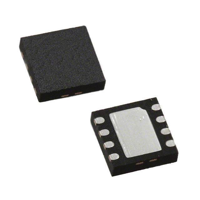
| 产品图片 |
|
| 产品型号 | AS1334-BTDT-30 |
| PWM类型 | 电流模式 |
| rohs | 无铅 / 符合限制有害物质指令(RoHS)规范要求 |
| 产品系列 | - |
| 供应商器件封装 | 8-TDFN(3x3) |
| 其它名称 | AS1334-BTDT-30CT |
| 包装 | 剪切带 (CT) |
| 同步整流器 | 是 |
| 安装类型 | 表面贴装 |
| 封装/外壳 | 8-WDFN 裸露焊盘 |
| 工作温度 | -40°C ~ 85°C |
| 标准包装 | 1 |
| 电压-输入 | 2.7 V ~ 5.5 V |
| 电压-输出 | 3V |
| 电流-输出 | 650mA |
| 类型 | 降压(降压) |
| 输出数 | 1 |
| 输出类型 | 固定 |
| 频率-开关 | 2MHz |





- 商务部:美国ITC正式对集成电路等产品启动337调查
- 曝三星4nm工艺存在良率问题 高通将骁龙8 Gen1或转产台积电
- 太阳诱电将投资9.5亿元在常州建新厂生产MLCC 预计2023年完工
- 英特尔发布欧洲新工厂建设计划 深化IDM 2.0 战略
- 台积电先进制程称霸业界 有大客户加持明年业绩稳了
- 达到5530亿美元!SIA预计今年全球半导体销售额将创下新高
- 英特尔拟将自动驾驶子公司Mobileye上市 估值或超500亿美元
- 三星加码芯片和SET,合并消费电子和移动部门,撤换高东真等 CEO
- 三星电子宣布重大人事变动 还合并消费电子和移动部门
- 海关总署:前11个月进口集成电路产品价值2.52万亿元 增长14.8%



PDF Datasheet 数据手册内容提取
austriamicrosystems AG is now ams AG The technical content of this austriamicrosystems datasheet is still valid. Contact information: Headquarters: ams AG Tobelbaderstrasse 30 8141 Unterpremstaetten, Austria Tel: +43 (0) 3136 500 0 e-Mail: ams_sales@ams.com Please visit our website at www.ams.com
Datasheet AS1334 650mA, Ultra low Ripple Step Down DC/DC Converter 1 General Description 2 Key Features d The AS1334 is a step-down DC-DC converter designed to power (cid:132) Output Voltage Ripple: 2mV portable applications from a single Li-Ion battery. The device also (cid:132) PWM Switching Frequency: 2MHz achieves high-performance in mobile phones and other applications i requiring low dropout voltage. (cid:132) Single Lithium-Ion Cell Operation l a The AS1334 operates from an input voltage range of 2.7 to 5.5V (cid:132) Output Voltage Range: 1.2V to 3.4V while providing output voltages of 1.2, 1.5, 1.8, 2.5, 3.0 and 3.3V. (available in 100mV steps, see Ordering Information on page 17) v Fixed-frequency PWM operation minimizes RF interference. (cid:132) Fixed Output Voltages: Shutdown function turns the device off and reduces battery - 1.2V, 1.5V, 1.8V, 2.5V, 3.0V, 3.3V consumption to 0.01µA (typ). (cid:132) Maximum Load Capability of 650mA l l The AS1334 is available in a TDFN(3x3) 8-pin package. A high (cid:132) 97% Hig h Efficiency, 94% Average Efificiency switching frequency (2 MHz) allows use of tiny surface-mount components. Only three small external surface-mount components, (cid:132) CurreGnt Overload Protection t s an inductor and two ceramic capacitors are required. (cid:132) Thermal Overload Protection A(cid:132) Power-OK (cid:132) Soft Start t n s (cid:132) Low Dropout Voltage (140 mΩ Typ PFET) (cid:132) TDFN(3xe3) 8-pin m 3 Atpplications n a The AS1334 is an ideal solution to supply noise sensitive oapplications as cellular phones, hand-held radios, RF PC cards, battery powered RF devices, RFID chipsets, A/D Converter, Sensors and OpAmps. c Figure 1. AS1334 - Typical Application Circuit l a c i VIN n PVIN SW 3.3 µH VOUT 10 µF h VDD FB AS1334 c 10 µF e ON EN POK OFF T PGND SGND www.austriamicrosystems.com/DC-DC_Step-Down/AS1334 Revision 1.09 1 - 18
AS1334 Datasheet - Pin Assignments 4 Pin Assignments Figure 2. Pin Configuration d i l a FB 1 8 PGND v POK 2 7 SW AS1334 l EN 3 6 PVIN l VDD 4 SGND 9 5 SGN D i G t s A t n s e m t 4.1 Pin Descriptions n a Table 1. Pin Descriptions o Pin Number Pin Name Description 1 FB Feedback Pin. Cocnnect to the output at the output filter capacitor. Power-OK. 2 POK 0 = VOUT < 90% of VOUTNOM. 1 = VOUTl > 90% of VOUTNOM. 3 EN Enabale Input. Set this digital input high for normal operation. For shutdown, set low. 4 VDD +2.7V to +5.5V Power Supply Voltage. Analog Supply Input. c 5, 9 SGND Analog and Control Ground. Connect these pins with low resistance to PGND. 6 PVIN i+2.7V to +5.5V Power Supply Voltage. Input to the internal PFET switch. n Switch Pin. Switch node connection to the internal PFET switch and NFET synchronous rectifier. 7 SW Connect to an inductor with a saturation current rating that exceeds the maximum switch peak h current limit specification of the AS1334. 8 PGND Power Ground. Connect this pin with low resistance to SGND. c e T www.austriamicrosystems.com/DC-DC_Step-Down/AS1334 Revision 1.09 2 - 18
AS1334 Datasheet - Absolute Maximum Ratings 5 Absolute Maximum Ratings Stresses beyond those listed in Table 2 may cause permanent damage to the device. These are stress ratings only, and functional operation of the device at these or any other conditions beyond those indicated in Electrical Characteristics on page 4 is not implied. Exposure to absolute maximum rating conditions for extended periods may affect device reliability. Table 2. Absolute Maximum Ratings d Parameter Min Max Units Notes i Electrical Parameters l VDD, PVIN to SGND -0.3 +7.0 V a PGND to SGND -0.3 +0.3 V v POK, EN, FB SGND - 0.3 VDD + 0.3 V 7.0V max SW PGND - 0.3 PVIN + 0.3 V l PVIN to VDD -0.3 +0.3 V l Input Voltage Range 2.7 5.5 V i G t Recommended Load Current 650 mA s In applications where high power dissipation and/ A or poor p ackage thermal resistance is present, the maximum ambient temperature may have to t be derated. nMaximum ambient temperature (TA-MAX) is s dependent on the maximum operating junction Ambient Temperature (TA) Range -40 +85 ºC etemperature (TJ-MAX-OP = 125ºC), the maximum power dissipation m t of the device in the application (PD-MAX), and the junction-to ambient thermal resistance of the n part/package in the application (θJA), as given by a the following o equation: TA-MAX = TJ-MAX-OP – (θJA × PD-MAX). Electrostatic Discharge c Human Body Model 2 kV Norm: MIL 883 E method 3015 Temperature Ranges and Storage Conditions Junction Temperature (TJ-MAX) l +150 ºC a Storage Temperature Range -55 +150 ºC c The reflow peak soldering temperature (body temperature) specified is in accordance with IPC/ i JEDEC J-STD-020“Moisture/Reflow Sensitivity Package Body Temperanture +260 ºC Classification for Non-Hermetic Solid State Surface Mount Devices”. The lead finish for Pb-free leaded packages is h matte tin (100% Sn). Humidity 5 86 % Non-condensing c Moisture Sensitive Level 1 Represents a max. floor life time of unlimited e T www.austriamicrosystems.com/DC-DC_Step-Down/AS1334 Revision 1.09 3 - 18
AS1334 Datasheet - Electrical Characteristics 6 Electrical Characteristics TA = TJ = -40ºC to +85ºC; PVIN = VDD = EN = 3.6V, unless otherwise noted. Typical values are at TA=25°C. Table 3. Electrical Characteristics Symbol Parameter Conditions Min Typ Max Units d TA Operating Temperature Range -40 +85 °C 1.176 1.2 1.224 V i l 1.47 1.5 1.53 V a 1.764 1.8 1.836 V VOUT Output Voltage PVIN = 3.6V v 2.45 2.5 2.55 V 2.94 3.0 3.06 V l 3.234 3.3 3.366 V l ISHDN Shutdown supply current EN = SW = 0V1 i0.01 2 µA G t IQ DC bias current into VDD FB = 0V, No Switching2 s 1 1.4 mA RDSON(P) Pin-Pin Resistance for PFET ISW = 200mA; ATA = +25°C 140 200 mΩ ISW = 200mA t 230 ISW = -200mA; TA = +25°C n 300 415 RDSON(N) Pin-Pin Resistance for NFET s mΩ ISW = -200mA 485 e ILIM,PFET Switch peak current limit m 935 1100 1200 mA t POK Output n VOL POK Output Low Voltage a POK sinking 0.1mA 0.05 0.2 V POK Output High Leakage Current POK = 3.6oV 500 nA POK Threshold Falling edge, referenced to VOUT(NOM) 87 90 93 % c Enable Input VIH,EN Logic high input threshold 1.2 V l VIL,EN Logic low input threshold a 0.5 V IPIN,ENABLE Pin pull down current 5 10 µA c Oscillator FOSC Internal oscillator freiquency 1.8 2 2.2 MHz n 1. Shutdown current includes leakage current of PFET. 2. IQ specified here is whehn the part is operating at 100% duty cycle. c e T www.austriamicrosystems.com/DC-DC_Step-Down/AS1334 Revision 1.09 4 - 18
AS1334 Datasheet - Electrical Characteristics 6.1 System Characteristics TA = 25ºC; PVIN = VDD = EN = 3.6V, unless otherwise noted. The following parameters are verified by characterisation and are not production tested. Table 4. System Characteristics Symbol Parameter Conditions Min Typ Max Units d Turn on time (from Enable low to high EN = Low to High, VIN = 4.2V, COUT = 10µF, T_ON transition) IOUT ≤ 1mA 210 350 µs i η Efficiency (L = 3.3µH, DCR ≤ 100mΩ) VIN = 3.6V, IOUT = 400mA 96 % l a VOUT_ripple Ripple voltage, PWM mode1 VIN = 4.2V, IOUT = 10mA to 400mA 5 mVp-p v VIN = 600mV perturbance, over VIN range 3.4V Line_tr Line transient response to 5.5V; TRISE = TFALL = 10µs, VOUT = 3.0V, 50 mVpk IOUT = 100mA l VIN = 4.2V, VOUT = 3.0V, transients up to l Load_tr Load transient response 50 mVpk 100mA, TRISE = TFALL = 10 µs i G t 1. Ripple voltage should measured at COUT electrode on good layout PC board and under condition using sugsgested inductors and capac- itors. A t Note: All limits are guaranteed. The parameters with min and max values are guaranteed with production tests or SQC (Statistical Quality n Control) methods. s e m t n a o c l a c i n h c e T www.austriamicrosystems.com/DC-DC_Step-Down/AS1334 Revision 1.09 5 - 18
AS1334 Datasheet - Typical Operating Characteristics 7 Typical Operating Characteristics Circuit in Figure 23 on page 11, PVIN = VDD = EN = 3.6V, L = 3.3µH (LPS4018-332ML_), CIN = COUT = 10µF (GRM21BR61C106KA01) unless otherwise noted. Figure 3. Quiescent Current vs. VIN Figure 4. Shutdown Current vs. Temperature 0.55 0.3 d Vin=3.25V Vin=3.6V 0.25 i mA) 0.5 µA) VViinn==45..25VV l urrent ( urrent ( 0.2 v a C0.45 C0.15 nt wn esce utdo 0.1 ll ui 0.4 h Q S i 0.05 - 45°C G t + 25°C + 85°C s 0.35 0 2.5 3 3.5 4 4.5 5 5.5 A -40 -15 1 0 35 60 85 Supply Voltage (V) Temperature (°C) t Figure 5. Switching Frequency Variation vs. Temperature Figure 6. Output Voltagen vs. Supply Voltage s 4 3.06 ) e % n ( 3 m 3.04 o t riati 2 V) n Va 1 a e (3.02 uency 0 oVoltag 3 ng Freq--21 c Output 2.98 hi l c Vin=3.6V 2.96 Iout=50mA wit-3 aVin=4.2V Iout=300mA S Vin=5.5V Iout=650mA -4 c 2.94 -40 -15 10 35 60 85 3.25 3.75 4.25 4.75 5.25 Temperaiture (°C) Supply Voltage (V) n h c e T www.austriamicrosystems.com/DC-DC_Step-Down/AS1334 Revision 1.09 6 - 18
AS1334 Datasheet - Typical Operating Characteristics Figure 7. Output Voltage vs. Temperature Figure 8. Efficiency vs. Output Current 3.06 100 3.04 95 V) e (3.02 %) 90 d Voltag 3 ency ( 85 i ut ci l utp2.98 Effi 80 Vin=3.25V a O Vin=3.6V Vin=3.9V v 2.96 Iout=50mA 75 Vin=4.2V Iout=300mA Vin=4.5V Iout=650mA Vin =5.5V 2.94 70 l -40 -15 10 35 60 85 0 100 200 300 400 50l0 600 700 Temperature (°C) Output Current (imA) G t s Figure 9. Switch Peak Current Limit vs. Temperature; closed loop Figure 10. Load Transient Response; VOUT = 3.0V, VIN = 4.2V A 1.2 t n mit (A)1.15 m s VOUT e 200mV/Div Li t ent 1.1 n Div urr a IL mA/ k C o 200 a e1.05 P A c m VViinn==23..76VV UT 400 O V in=5.5V I A 1 m l 0 0 -40 -15 10 35 a60 85 10µs/Div 1 Temperature (°C) c i Figure 11. Startup; VIN = 3.6V, VOUT = 3.0V, IOUT<1mA, Figure 12. Startup; VIN = 4.2V, VOUT = 3.0V, IOUT<1mA, RLOAD=3.3kΩ n RLOAD=3.3kΩ h W c Div W Div VS 5V/ VS 5V/ VOUT T e 2V/Div VOUT 2V/Div V V DI DI A/ A/ m m IL 500 IL 500 EN 2V/Div EN 1V/Div 50µs/Div 50µs/Div www.austriamicrosystems.com/DC-DC_Step-Down/AS1334 Revision 1.09 7 - 18
AS1334 Datasheet - Typical Operating Characteristics Figure 13. Shutdown Response; VIN=3.6V, VOUT=3.0V, Figure 14. Shutdown Response; VIN=4.2V, VOUT=3.0V, RLOAD=5Ω RLOAD=5Ω VSW 5V/Div VSW 5V/Div d VOUT 2V/Div VOUT 2V/Div li a IL 500mA/Div IL v500mA/Div EN 2V/Div EN l 2V/Div l 50µs/Div 50µs/Div i G t s Figure 15. Line Transient Response; VIN=3.3V to 3.9V, Figure 16. Timed Current Limit Response; VIN=3.6V, VOUT=3.0V IOUT=100mA, VOUT=3.0V A t n s VIN m 1V/Div VSW e 2V/Div t n a Div IL 100mA/ oVOUT 2V/Div c OUT mV/Div IL 2A/Div V 0 l5 a 10µs/Div 50µs/Div c i Figure 17. Output Voltage Ripple; VOUT = 3.0V, IOUT = 200mA Figure 18. VOUT Ripple in Skip Mode; VIN=3.31V, VOUT=3.0V, n RLOAD=5Ω h VSW c 2V/Div VSW 2V/Div e T Div Div A/ A/ IL 100m IL 200m VOUT 5mV/Div VOUT 0mV/Div 1 200ns/Div 1µs/Div www.austriamicrosystems.com/DC-DC_Step-Down/AS1334 Revision 1.09 8 - 18
AS1334 Datasheet - Typical Operating Characteristics Figure 19. RDSON (P-Channel) vs. Temp.; ISW=200mA Figure 20. RDSON (N-Channel) vs. Temp.; ISW=-200mA 350 350 300 300 250 250 Ωm )200 Ωm )200 d (N (N i SO150 SO150 l D D R R a 100 100 v Vin=2.7V Vin=2.7V 50 50 Vin=3.6V Vin=3.6V Vin=5.5V Vin=5.5 V 0 0 l -40 -15 10 35 60 85 -40 -15 10 35 l60 85 Temperature (°C) Temperature (°iC) G t s Figure 21. EN High Threshold vs. VIN A 1.2 t 1.15 n s d (V) 1.1 e ol1.05 m sh t e hr 1 n T h a g0.95 Hi o N 0.9 E c - 45°C 0.85 + 25°C + 90°C 0.8 l 2.5 3 3.5 4 4.5 a5 5.5 Supply Voltage (V) c i n h c e T www.austriamicrosystems.com/DC-DC_Step-Down/AS1334 Revision 1.09 9 - 18
AS1334 Datasheet - Detailed Description 8 Detailed Description The AS1334 is a simple, step-down DC-DC converter optimized for powering portable applications that require low dropout voltages such as mobile phones, portable communicators, and similar battery powered RFID devices. Besides being packed with numerous features like current overload protection, thermal overload shutdown and soft start, AS1334 displays the following characteristics: (cid:132) Its operation is based on current-mode buck architecture with synchronous rectification for high efficiency. d (cid:132) Allows the application to operate at maximum efficiency over a wide range of power levels from a single Li-Ion battery cell. (cid:132) Provides for a maximum load capability of 650mA in PWM mode, wherein the maximum load range may vary depending on input voltage, i output voltage and the selected inductor. l a (cid:132) Is ranked at an efficiency of around 96% for a 400mA load with a 3.6V input voltage. v Figure 22. AS1334 - Functional Block Diagram l l i G t s POK VDD PVIN A t 1.13V – + Oscillator n s e Current m Sense FB t AmplifieraError COMPPWM n o Mosfet SW Control c Logic Soft Start l a Main Control c EN Shutdown iControl AS1334 n h SGND PGND c e T The size of the external components is reduced by using a high switching frequency (2MHz). Figure 1 on page 1 demonstrates that only three external power components are required for implementation. Also, the system controller should set EN low during power-up and other low supply voltage conditions. See Shutdown Mode on page 12. www.austriamicrosystems.com/DC-DC_Step-Down/AS1334 Revision 1.09 10 - 18
AS1334 Datasheet - Detailed Description Figure 23. Typical Operating System Circuit d i VIN PVIN SW 3.3 µH VOUT l 2.7V to 5.5V a 10 µF VDD FB v AS1334 10 µF l System Con- EN POK l troller i ON/OFF G t s PGND SGND A t n s e m t n a 8.1 Operating the AS1334 o AS1334’s control block turns on the internal PFET (P-channel MOSFET) switch during the first part of each switching cycle, thus allowing current to flow from the input through the inductor to the output filter capcacitor and load. The inductor limits the current to a ramp with a slope of around (VIN - VOUT) / L, by storing energy in a magnetic field. During the second part of each cycle, the controller turns the PFET switch off, blocking current flow from the input, and then turns the NFET (N- channel MOSFET) synchronous rectifier on. As a resullt, the inductor’s magnetic field collapses, generating a voltage that forces current from ground through the synchronous rectifier to the outaput filter capacitor and load. While the stored energy is transferred back cinto the circuit and depleted, the inductor current ramps down with a slope around VOUT / L. The output filter capacitor stores charge when the inductor current is high, and releases it when low, smoothing the voltage across the load. The output voltage is regulated by modulating the PFET switch on time to control the average current sent to the load. The effect is identical to i sending a duty-cycle modulated rectangular wave formed by the switch and synchronous rectifier at SW to a low-pass filter formed by the n inductor and output filter capacitor. The output voltage is equahl to the average voltage at the SW pin. While in operation, the output voltage is regulated by switching at a constant frequency and then modulating the energy per cycle to control power to the load. Ecnergy per cycle is set by modulating the PFET switch on-time pulse width to control the peak inductor current. This is done by comparing the signal from the current-sense amplifier with a slope compensated error signal from the voltage-feedback error amplifier. At the beginning of eeach cycle, the clock turns on the PFET switch, causing the inductor current to ramp up. When the current sense signal ramps past the error amplifier signal, the PWM comparator turns off the PFET switch and turns on the NFET synchronous rectifier, ending the first part of the cycle.T If an increase in load pulls the output down, the error amplifier output increases, which allows the inductor current to ramp higher before the comparator turns off the PFET. This increases the average current sent to the output and adjusts for the increase in the load. Before appearing at the PWM comparator, a slope compensation ramp from the oscillator is subtracted from the error signal for stability of the current feedback loop. The minimum on time of PFET in PWM mode is 50ns (typ). www.austriamicrosystems.com/DC-DC_Step-Down/AS1334 Revision 1.09 11 - 18
AS1334 Datasheet - Detailed Description 8.2 Internal Synchronous Rectifier To reduce the rectifier forward voltage drop and the associated power loss, the AS1334 uses an internal NFET as a synchronous rectifier. The big advantage of a synchronous rectification is the higher efficiency in a condition where the output voltage is low compared to the voltage drop across an ordinary rectifier diode. During the inductor current down slope in the second part of each cycle the synchronous rectifier is turned on. Before the next cycle the synchronous rectifier is turned off. There is no need for an external diode because the NFET is conducting through its intrinsic body diode during the transient intervals before it d turns on. i 8.3 Power-OK l The POK output indicates if the output voltage is within 90% of the nominal voltage level. As long as the output voltage is within regulation thea open-drain POK output sinks current. v 8.4 Shutdown Mode If EN is set to high (>1.2V) the AS1334 is in normal operation mode. During power-up and when the power supply is less than 2.7V minimum l operating voltage, the chip should be turned off by setting EN low. In shutdown mode the following blocks of the AS1334 lare turned off, PFET switch, NFET synchronous rectifier, reference voltage source, control and bias circuitry. T he AS1334 is designed for ciompact portable applications, such as mobile phones where the system controller controls operation mGode for maximizing battery lifte and requirements for small package size outweigh the additional size required for inclusion of UVLO (Under Voltage Lock-Out) circuitry. s Note: Setting the EN digital pin low (<0.5V) places the AS1334 in a 0.01µA (typ) shutdown mode. A t 8.5 Thermal Overload Protection n To prevent the AS1334 from short-term misuse and overload conditions the chip includes a thermal overload protection. To block the normal s operation mode the device is turning the PFET and the NFET off in PWM mode as soon as the junction temperature exceeds 150°C. To resume e normal operation the temperature has to drop below 140°C. m t Note: Continuing operation in thermal overload conditions may damage the device and is considered bad practice. n 8.6 Current Limiting For Protecation o If in the PWM mode the cycle-by-cycle current limit of 1200mA (max.) is reached the current limit feature takes place and protects the device and the external components. A timed current limiting mode is working when a load pulls the output voltage down to approximately 0.375V. In this c timed current limit mode the inductor current is forced to ramp down to a safe value. This is achieved by turning off the internal PFET switch and delaying the start of the next cycle for 3.5us. The synchronous rectifier is also turned off in the timed current limit mode. The advantage of the timed current limit mode is to prlevent the device from the loss of the current control. a c i n h c e T www.austriamicrosystems.com/DC-DC_Step-Down/AS1334 Revision 1.09 12 - 18
AS1334 Datasheet - Application Information 9 Application Information 9.1 Inductor Selection For the external inductor, a 3.3µH inductor is recommended. Minimum inductor size is dependant on the desired efficiency and output current. Inductors with low core losses and small DCR at 2MHz are recommended. d Table 5. Recommended Inductor i Part Number L DCR Current Rating Dimensions (L/W/T) Manufacturer l LPS4018-222ML_ 2.2µH 0.070Ω 2.9A 3.9x3.9x1.7mm Coilcraft a www.coilcraft.com LPS4018-332ML_ 3.3µH 0.080Ω 2.4A 3.9x3.9x1.7mm v LPS4018-472ML_ 4.7µH 0.125Ω 1.9A 3.9x3.9x1.7mm 9.2 Capacitor Selection l A 10µF capacitor is recommended for CIN as well as a 10µF for COUT. Small-sized X5R or X7R ceramic capacitors are lrecommended as they retain capacitance over wide ranges of voltages and temperatures. i G t 9.2.1 Input and Output Capacitor Selection s Low ESR input capacitors reduce input switching noise and reduce the peak current drawn from the battery. Also low ESR capacitors should be used to minimize VOUT ripple. Multi-layer ceramic capacitors are recommenAded since they have extrem ely low ESR and are available in small footprints. t n For input decoupling the ceramic capacitor should be located as close to the device as practical. A 4.7µF input capacitor is sufficient for most s applications. Larger values may be used without limitations. e A 2.2µF to 10µF output ceramic capacitor is sufficient for most applications. Larger values up to 22µF may be used to obtain extremely low out- m put voltage ripple and improve transient response. t n Table 6. Recommended Input and Output Capaacitor Part Number C TC Code Ratoed Voltage Dimensions (L/W/T) Manufacturer GRM188R60J475KE19 4.7µF X5R 6.3V 0603 Murata c www.murata.com GRM219R60J475KE19 4.7µF X5R 6.3V 0805 GRM21BR61C475KA88 4.7µF X 5R 16V 0805 GRM31CR71E475KA88 4.7µF lX7R 25V 1206 a GRM188R60J106ME47 10µF X5R 6.3V 0603 GRM21BR60J106KE19 10µFc X5R 6.3V 0805 GRM21BR61A106KE19 10µF X5R 10V 0805 i GRM32DR71C106KA01 10µF X7R 16V 1210 n GRM21BR60J226ME39 22µF X5R 6.3V 0805 GRM32ER71A226KEh20 22µF X7R 10V 1210 9.3 EN Pin Ccontrol Drive the EN pin using the system controller to turn the AS1334 ON and OFF. Use a comparator, Schmidt trigger or logic gate to drive the EN pin. e Set EN high (>1.2V) for normal operation and low (<0.5V) for a 0.01µA (typ) shutdown mode. Set EN low to turn off the AS1334 during power-up and under voltage conditions when the power supply is less than the 2.7V minimum operating voltage. The part is out of regulation when the T input voltage is less than 2.7V. www.austriamicrosystems.com/DC-DC_Step-Down/AS1334 Revision 1.09 13 - 18
AS1334 Datasheet - Application Information 9.4 Layout Considerations The AS1334 converts higher input voltage to lower output voltage with high efficiency. This is achieved with an inductor based switching topology. During the first half of the switching cycle, the internal PMOS switch turns on, the input voltage is applied to the inductor, and the current flows from PVDD line to the output capacitor (C2) through the inductor. During the second half cycle, the PMOS turns off and the internal NMOS turns on. The inductor current continues to flow via the inductor from the device PGND line to the output capacitor (C2). Referring to Figure 24, the AS1334 has two major current loops where pulse and ripple current flow. The loop shown in the left hand side is most important, d because pulse current shown in Figure 24 flows in this path. The right hand side is next. The current waveform in this path is triangular, as shown in Figure 24. Pulse current has many high-frequency components due to fast di/dt. Triangular ripple current also has wide high-frequency components. Board layout and circuit pattern design of these two loops are the key factors for reducing noise radiation and stable operation. i Other lines, such as from battery to C1(+) and C2(+) to load, are almost DC current, so it is not necessary to take so much care. Only pattern l width (current capability) and DCR drop considerations are needed. a Figure 24. Current Loop v l l i G t s VIN i 3.25V to 5.5V A fOSC = 2MHz i t + C1 PVIN VDD - 10 µF n L1 s 3.3 µH e VOUT EN m SW t n a FB C2 + o 10 µF - c PGND SGND POK l a c i n h c e T www.austriamicrosystems.com/DC-DC_Step-Down/AS1334 Revision 1.09 14 - 18
AS1334 Datasheet - Package Drawings and Markings 10 Package Drawings and Markings Figure 25. TDFN(3x3) 8-pin Marking d i l a v Table 7. Packaging Code YYWWQZZ l l YY WW Q ZZ i year identifier manufacturing week plant identifieGr free choice / traceatbility code s A t n s e m t n a o c l a c i n h c e T www.austriamicrosystems.com/DC-DC_Step-Down/AS1334 Revision 1.09 15 - 18
AS1334 Datasheet - Package Drawings and Markings Figure 26. TDFN(3x3) 8-pin Package d i l a v l l i G t s A t n s e m t n a o c l a c i n h c e T www.austriamicrosystems.com/DC-DC_Step-Down/AS1334 Revision 1.09 16 - 18
AS1334 Datasheet - Ordering Information 11 Ordering Information The device is available as the standard products shown in Table 8. Table 8. Ordering Information Ordering Code Marking Output Description Delivery Form Package d 650mA, Ultra low Ripple Step Down DC/DC AS1334-BTDT-12 ASR2 1.2V Tape and Reel TDFN(3x3) 8-pin Converter i 650mA, Ultra low Ripple Step Down DC/DC AS1334-BTDT-15 ASR3 1.5V Converter Tape and Reel TDFN(3x3) 8-pin l a 650mA, Ultra low Ripple Step Down DC/DC AS1334-BTDT-18 ASR4 1.8V Tape and Reel TDFN(3x3) 8-pin Converter v 650mA, Ultra low Ripple Step Down DC/DC AS1334-BTDT-25 ASR5 2.5V Tape and Reel TDFN(3x3) 8-pin Converter 650mA, Ultra low Ripple Step Down DC/DC AS1334-BTDT-30 ASQY 3.0V Converter Tape and Reel lTDFN(3x3) 8-pin l 650mA, Ultra low Ripple Step Down DC/DC AS1334-BTDT-33 ASR6 3.3V Converter Tape and Reeil TDFN(3x3) 8-pin G t AS1334-BTDT-xx1 xxxx xxxx 650mA, Ultra lowC Roinpvpelert eSrtep Down DC/DC Tape asnd Reel TDFN(3x3) 8-pin 1. Non-standard devices are available between 1.2V and 3.4V in 100mV steAps. For more information an d inquiries contact http://www.aus- triamicrosystems.com/contact t n Note: All products are RoHS compliant. s Buy our products or get free samples online at ICdirect: http://www.austriamicrosystems.com/ICdirect e m Technical Support is found at http://www.austriamicrosystems.com/Technical-Support t n For further information and requests, please contact us mailto:sales@austriamicrosystems.com a or find your local distributor at http://www.austriamicrosystems.com/distributor o Design the AS1334 online at http://www.austriamicrosystems.com/analogbench analogbench is a powerful design and simulation supcport tool that operates in on-line and off-line mode to evaluate performance and generate application-specific bill-of-materials for austriamicrosystems' power management devices. l a c i n h c e T www.austriamicrosystems.com/DC-DC_Step-Down/AS1334 Revision 1.09 17 - 18
AS1334 Datasheet Copyrights Copyright © 1997-2010, austriamicrosystems AG, Tobelbaderstrasse 30, 8141 Unterpremstaetten, Austria-Europe. Trademarks Registered ®. All rights reserved. The material herein may not be reproduced, adapted, merged, translated, stored, or used without the prior written consent of the copyright owner. All products and companies mentioned are trademarks or registered trademarks of their respective companies. d Disclaimer i l Devices sold by austriamicrosystems AG are covered by the warranty and patent indemnification provisions appearing in its Term of Sale. a austriamicrosystems AG makes no warranty, express, statutory, implied, or by description regarding the information set forth herein or regarding the freedom of the described devices from patent infringement. austriamicrosystems AG reserves the right to change specifications and prices at v any time and without notice. Therefore, prior to designing this product into a system, it is necessary to check with austriamicrosystems AG for current information. This product is intended for use in normal commercial applications. Applications requiring extended temperature range, unusual environmental requirements, or high reliability applications, such as military, medical life-support or life-sustaining equipment are l specifically not recommended without additional processing by austriamicrosystems AG for each application. For shipments of less than 100 l parts the manufacturing flow might show deviations from the standard production flow, such as test flow or test location. i The information furnished here by austriamicrosystems AG is believed to be correct aGnd accurate. However, austritamicrosystems AG shall not be liable to recipient or any third party for any damages, including but not limited to personal injury, property dasmage, loss of profits, loss of use, interruption of business or indirect, special, incidental or consequential damages, of any kind, in connection with or arising out of the furnishing, performance or use of the technical data herein. No obligation or liability to rAecipient or any third party sh all arise or flow out of austriamicrosystems AG rendering of technical or other services. t n s e m t n a o c l a c Contact Information i n Headquarters austriamicrosystems AG h Tobelbaderstrasse 30 A-8141 Unterpremstaetten, Austria c Tel: +43 (0) 3136 500 0 Fax: +43 (0) e3136 525 01 T For Sales Offices, Distributors and Representatives, please visit: http://www.austriamicrosystems.com/contact www.austriamicrosystems.com/DC-DC_Step-Down/AS1334 Revision 1.09 18 - 18
 Datasheet下载