ICGOO在线商城 > 集成电路(IC) > PMIC - 稳压器 - DC DC 开关稳压器 > AS1310-BTDT-30
 Datasheet下载
- 型号: AS1310-BTDT-30
- 制造商: AUSTRIAMICROSYSTEMS
- 库位|库存: xxxx|xxxx
- 要求:
| 数量阶梯 | 香港交货 | 国内含税 |
| +xxxx | $xxxx | ¥xxxx |
查看当月历史价格
查看今年历史价格
AS1310-BTDT-30产品简介:
ICGOO电子元器件商城为您提供AS1310-BTDT-30由AUSTRIAMICROSYSTEMS设计生产,在icgoo商城现货销售,并且可以通过原厂、代理商等渠道进行代购。 AS1310-BTDT-30价格参考。AUSTRIAMICROSYSTEMSAS1310-BTDT-30封装/规格:PMIC - 稳压器 - DC DC 开关稳压器, 固定 升压 开关稳压器 IC 正 3V 1 输出 320mA(开关) 8-UFDFN 裸露焊盘。您可以下载AS1310-BTDT-30参考资料、Datasheet数据手册功能说明书,资料中有AS1310-BTDT-30 详细功能的应用电路图电压和使用方法及教程。
AS1310-BTDT-30 是奥地利微电子(ams)公司推出的一款 DC-DC 开关稳压器,主要应用于需要高效、小尺寸电源解决方案的场景。该器件具有高效率、低静态电流和宽输入电压范围等特点,适用于以下应用场景:

1. 便携式电子设备:如智能手机、平板电脑、可穿戴设备等,适用于电池供电系统,延长电池寿命。

2. 工业控制系统:用于传感器、执行器、PLC 等设备中,提供稳定电源,适应复杂工业环境。

3. 汽车电子:如车载导航、信息娱乐系统、仪表盘模块等,支持宽电压输入,适应车辆电源波动。

4. 通信设备:适用于无线基站、路由器、接入设备等,提供高效、稳定的电源转换。

5. 医疗设备:如便携式监护仪、诊断设备等,确保低功耗与高可靠性。

该器件采用小型封装,节省PCB空间,适合高密度布局设计。其固定输出电压版本(3.0V)适用于为低功耗MCU、RF模块、传感器等提供主电源。
| 参数 | 数值 |
| 产品目录 | 集成电路 (IC)半导体 |
| 描述 | IC REG BOOST 3V 60MA 8TDFN稳压器—开关式稳压器 DC-DC Converter |
| 产品分类 | |
| 品牌 | ams |
| 产品手册 | |
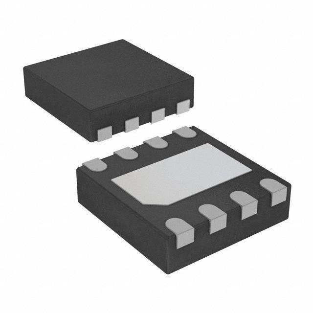
| 产品图片 |
|
| rohs | 符合RoHS无铅 / 符合限制有害物质指令(RoHS)规范要求 |
| 产品系列 | 电源管理 IC,稳压器—开关式稳压器,ams AS1310-BTDT-30- |
| 数据手册 | http://www.ams.com/eng/content/download/78582/596791/48756 |
| 产品型号 | AS1310-BTDT-30 |
| PWM类型 | - |
| 产品种类 | 稳压器—开关式稳压器 |
| 供应商器件封装 | 8-TDFN(2x2) |
| 其它名称 | AS1310-BTDT-30DKR |
| 包装 | Digi-Reel® |
| 同步整流器 | 无 |
| 商标 | ams |
| 安装类型 | 表面贴装 |
| 安装风格 | SMD/SMT |
| 封装 | Reel |
| 封装/外壳 | 8-UFDFN 裸露焊盘 |
| 封装/箱体 | TDFN-8 |
| 工作温度 | -40°C ~ 85°C |
| 工厂包装数量 | 1000 |
| 拓扑结构 | Boost |
| 最大工作温度 | + 85 C |
| 最大输入电压 | 3.6 V |
| 最小工作温度 | - 40 C |
| 最小输入电压 | 0.7 V |
| 标准包装 | 1 |
| 电压-输入 | 0.7 V ~ 3.6 V |
| 电压-输出 | 3V |
| 电流-输出 | 60mA |
| 电源电流 | 1 uA |
| 类型 | Step-Up DC/DC Converter |
| 输出数 | 1 |
| 输出电压 | 3 V |
| 输出电流 | 60 mA |
| 输出端数量 | 1 Output |
| 输出类型 | 固定 |
| 频率-开关 | - |


- 商务部:美国ITC正式对集成电路等产品启动337调查
- 曝三星4nm工艺存在良率问题 高通将骁龙8 Gen1或转产台积电
- 太阳诱电将投资9.5亿元在常州建新厂生产MLCC 预计2023年完工
- 英特尔发布欧洲新工厂建设计划 深化IDM 2.0 战略
- 台积电先进制程称霸业界 有大客户加持明年业绩稳了
- 达到5530亿美元!SIA预计今年全球半导体销售额将创下新高
- 英特尔拟将自动驾驶子公司Mobileye上市 估值或超500亿美元
- 三星加码芯片和SET,合并消费电子和移动部门,撤换高东真等 CEO
- 三星电子宣布重大人事变动 还合并消费电子和移动部门
- 海关总署:前11个月进口集成电路产品价值2.52万亿元 增长14.8%


PDF Datasheet 数据手册内容提取
AS1310 Ultra Low Quiescent Current, Hysteretic DC-DC Step-Up Converter General Description The AS1310 is an ultra low quiescent current hysteretic step-up DC-DC converter optimized for light loads (60mA), where it achieves efficiencies of up to 92%. AS1310 operates from a 0.7V to 3.6V supply and supports output voltages between 1.8V and 3.3V. Besides the available AS1310 standard variants any variant with output voltages in 50mV steps are available. If the input voltage exceeds the output voltage the device is in a feed-through mode and the input is directly connected to the output voltage. In light load operation, the device enters a sleep mode when most of the internal operating blocks are turned OFF in order to save power. This mode is active approximately 50μs after a current pulse provided that the output is in regulation. In order to save power the AS1310 features a shutdown mode, where it draws less than 100nA. During shutdown mode the battery is disconnected from the output. The AS1310 also offers adjustable low battery detection. If the battery voltage decreases below the threshold defined by two external resistors on pin LBI, the LBO output is pulled to logic low. The AS1310 is available in a TDFN (2x2) 8-pin package. OrderingInformation and ContentGuide appear at end of datasheet. Key Benefits & Features The benefits and features of AS1310, Ultra Low Quiescent Current, Hysteretic DC-DC Step-Up Converter are listed below: Figure 1: Added Value of Using AS1310 Benefits Features Ideal for single Li-Ion battery powered • Wide Input Voltage Range (0.7V to 3,6V) applications • Feed through mode when V > V IN OUT • High Efficiency up to 92% Extended battery life • Low Quiescent Current of typ. 1uA • Low Shutdown Current of less than 100nA • Fixed output voltage range (1.8V to 3.3V) Supports a variety of end applications • Output Disconnect in shutdown • Output current: 60mA @ VIN=0.9V, VOUT=1.8V ams Datasheet Page 1 [v1-11] 2015-Jan-28 DocumentFeedback
AS1310 − General Description Benefits Features Over – temperature protection and Integrated temperature monitoring shutdown Early power-fail warning Adjustable low battery detection • No external diode or transistor required Cost effective, small package • 8-pin TDFN (2mm x 2mm) Applications The AS1310 is an ideal solution for single and dual cell powered devices as blood glucose meters, remote controls, hearing aids, wireless mouse or any light-load application. Figure 2: Typical Application Diagram L1 6.8μH VIN 3 LX 0.7V to 3.6V Low Battery Detect 8 6 VIN LBO C1 R1 R3 22μF 1 4 VOUT AS1310 1.8V to 3.3V LBI VOUT R2 C2 22μF On 7 5 Off EN REF CREF 100nF 2 GND Page 2 ams Datasheet DocumentFeedback [v1-11] 2015-Jan-28
AS1310 − Pin Assignment Pin Assignment Figure 3: Pin Diagram (Top View) LBI 1 8 VIN GND 2 7 EN AS1310 LX 3 6 LBO VOUT 4 Exposed pad 5 REF Figure 4: Pin Description Pin Number Pin Name Description Low Battery Comparator Input. 0.6V Threshold. May not be left floating. If 1 LBI connected to GND, LBO is working as Power Output OK. 2 GND Ground 3 LX External Inductor Connector Output Voltage. Decouple V with a ceramic capacitor as close as 4 V OUT OUT possible to V and GND. OUT 5 REF Reference Pin. Connect a 100nF ceramic capacitor to this pin. 6 LBO Low Battery Comparator Output. Open-drain output. Enable Pin. Logic controlled shutdown input. 7 EN 1 = Normal operation; 0 = Shutdown; shutdown current <100nA. Battery Voltage Input. Decouple V with a 22μF ceramic capacitor as 8 V IN IN close as possible to V and GND. IN Exposed Pad. This pad is not connected internally. Can be left floating or 9 NC connect to GND to achieve an optimal thermal performance. ams Datasheet Page 3 [v1-11] 2015-Jan-28 DocumentFeedback
AS1310 − Absolute Maximum Ratings Absolute Maximum Ratings Stresses beyond those listed in Absolute Maximum Ratings may cause permanent damage to the device. These are stress ratings only, and functional operation of the device at these or any other conditions beyond those indicated in Electrical Characteristics is not implied. Exposure to absolute maximum rating conditions for extended periods may affect device reliability. Figure 5: Absolute Maximum Ratings Parameter Min Max Units Comments Electrical Parameters V , V , EN, LBI, LBO to GND -0.3 +5 V IN OUT LX, REF to GND -0.3 V + 0.3 V OUT Input Current (latch-up -100 100 mA Norm: JEDEC 78 immunity) Electrostatic Discharge Electrostatic Discharge HBM ±2 kV Norm: MIL 883 E method 3015 Temperature Ranges and Storage Conditions Thermal Resistance θ 58 ºC/W JA Junction Temperature +125 ºC Storage Temperature Range -55 +125 ºC The reflow peak soldering temperature (body temperature) specified is in accordance with IPC/JEDEC J-STD-020“Moisture/Reflow Package Body Temperature +260 ºC Sensitivity Classification for Non-Hermetic Solid State Surface Mount Devices”. The lead finish for Pb-free leaded packages is matte tin (100% Sn). Humidity non-condensing 5 85 % Represents a maximum floor life Moisture Sensitive Level 1 time of unlimited Page 4 ams Datasheet DocumentFeedback [v1-11] 2015-Jan-28
AS1310 − Electrical Characteristics Electrical Characteristics All limits are guaranteed. The parameters with Min and Max values are guaranteed by production tests or SQC (Statistical Quality Control) methods. V = 1.5V, C1 = C2 = 22μF, C = 100nF, Typical values are at IN REF T = +25ºC (unless otherwise specified). All limits are AMB guaranteed. The parameters with min and max values are guaranteed with production tests or SQC (Statistical Quality Control) methods. Figure 6: Electrical Characteristics Symbol Parameter Conditions Min Typ Max Units Operating Temperature T -40 +85 °C AMB Range Input V Input Voltage Range 0.7 3.6 V IN Minimum Startup Voltage I = 1mA, T = +25°C 0.7 0.8 V LOAD AMB Regulation V Output Voltage Range 1.8 3.3 V OUT I = 10 mA, T = +25°C -2 +2 % LOAD AMB Output Voltage Tolerance I = 10mA -3 +3 % LOAD V Lockout Threshold(1) Rising Edge 1.55 1.65 1.75 V OUT Operating Current V = 1.02xV , OUT OUTNOM Quiescent Current V REF = 0.99xV , 100 nA IN OUTNOM T = +25°C AMB I Q V = 1.02xV , REF = OUT ON Quiescent Current V 0.99xV , 0.8 1 1.2 μA OUT ON No load, T = +25°C AMB I Shutdown Current T = +25ºC 100 nA SHDN AMB ams Datasheet Page 5 [v1-11] 2015-Jan-28 DocumentFeedback
AS1310 − Electrical Characteristics Symbol Parameter Conditions Min Typ Max Units Switches NMOS 0.35 Ω R V = 3V ON OUT PMOS 0.5 Ω NMOS maximum On-time 3.6 4.2 4.8 μs I Peak Current Limit 320 400 480 mA PEAK Zero Crossing Current 5 20 35 mA Enable, Reference VENH EN Input Voltage High 0.7 V VENL EN Input Voltage Low 0.1 V I EN Input Bias Current EN = 3.6V, T = +25°C 100 nA EN AMB REF = 0.99xV , I REF Input Bias Current OUTNOM 100 nA REF T = +25°C AMB Low Battery & Power-OK V LBI Threshold Falling Edge 0.57 0.6 0.63 V LBI LBI Hysteresis 25 mV I LBI Leakage Current LBI = 3.6V, T = +25°C 100 nA LBI AMB VLBO LBO Voltage Low (2) ILBO = 1mA 20 100 mV I LBO Leakage Current LBO = 3.6V, T = +25°C 100 nA LBO AMB Power-OK Threshold LBI = 0V, Falling Edge 90 92.5 95 % Thermal Protection Thermal Shutdown 10°C Hysteresis 150 °C Note(s) and/or Footnote(s): 1. The regulator is in startup mode until this voltage is reached. Caution: Do not apply full load current until the device output > 1.75V. 2. LBO goes low in startup mode as well as during normal operation if: - The voltage at the LBI pin is below LBI threshold. - The voltage at the LBI pin is below 0.1V and V is below 92.5% of its nominal value. OUT Page 6 ams Datasheet DocumentFeedback [v1-11] 2015-Jan-28
AS1310 − Typical Operating Characteristics Typical Operating T = +25°C, unless otherwise specified. AMB Characteristics Figure 7: Efficiency vs. Output Current; V = 1.8V OUT 90 85 L1: XPL2010-682M 80 75 ) % (70 y c n65 e ci60 Effi 55 50 Vin = 0.9V Vin = 1.2V 45 Vin = 1.5V 40 0.01 0.1 1 10 100 1000 Output Current (mA) Figure 8: Efficiency vs. Output Current; V = 1.8V OUT 90 L1: XPL7030-682M 85 80 75 ) % (70 y c n65 e ci60 Effi 55 50 Vin = 0.9V Vin = 1.2V 45 Vin = 1.5V 40 0.01 0.1 1 10 100 1000 Output Current (mA) ams Datasheet Page 7 [v1-11] 2015-Jan-28 DocumentFeedback
AS1310 − Typical Operating Characteristics Figure 9: Efficiency vs. Output Current; V = 3.0V OUT 100 L1: XPL2010-682M 95 90 85 ) 80 % y ( 75 c n 70 e ci 65 Effi 60 Vin = 0.9V 55 Vin = 1.2V Vin = 1.5V 50 Vin = 1.8V 45 Vin = 2.4V 40 0.01 0.1 1 10 100 1000 Output Current (mA) Figure 10: Efficiency vs. Output Current; V = 3.0V OUT 100 L1: XPL7030-682M 95 90 85 ) 80 % y ( 75 c n 70 e ci 65 Effi 60 Vin = 0.9V 55 Vin = 1.2V 50 Vin = 1.5V Vin = 1.8V 45 Vin = 2.4V 40 0.01 0.1 1 10 100 1000 Output Current (mA) Page 8 ams Datasheet DocumentFeedback [v1-11] 2015-Jan-28
AS1310 − Typical Operating Characteristics Figure 11: Efficiency vs. Input Voltage; V = 1.8V OUT 100 L1: XPL2010-682M 95 90 85 ) % ( 80 y c n 75 e Effici 70 65 60 Iout = 1mA 55 Iout=10mA Iout=50mA 50 0.7 0.9 1.1 1.3 1.5 1.7 1.9 Input Voltage (V) Figure 12: Maximum Output Current vs. Input Voltage 180 160 ) .140 A m120 ( t n100 e r r u C 80 t u p 60 t u O 40 Vout = 1.8V 20 Vout = 3.0V 0 0 0.5 1 1.5 2 2.5 3 Input Voltage (V) ams Datasheet Page 9 [v1-11] 2015-Jan-28 DocumentFeedback
AS1310 − Typical Operating Characteristics Figure 13: Start-up Voltage vs. Output Current 1 0.95 0.9 ) V (0.85 e g a 0.8 t ol V0.75 p u 0.7 - rt a0.65 St 0.6 0.55 0.5 0 1 2 3 4 5 6 7 8 9 10 Output Current (mA) Figure 14: RON vs. Temperature 1 0.9 0.8 0.7 Ω ( ) 00..56 N O R 0.4 0.3 0.2 PMOS 0.1 NMOS 0 -40 -15 10 35 60 85 Temperature (°C) Page 10 ams Datasheet DocumentFeedback [v1-11] 2015-Jan-28
AS1310 − Typical Operating Characteristics Figure 15: Output Voltage Ripple; V = 2V, V = 3V,R = 100Ω IN OUT load LX Div V V/ 2 v X Di IL mA/ 0 0 2 C) A v (VOUT 00mV/Di 1 5μs/Div ams Datasheet Page 11 [v1-11] 2015-Jan-28 DocumentFeedback
AS1310 − Detailed Description Detailed Description Hysteretic Boost Converter Hysteretic boost converters are so called because comparators are the active elements used to determine ON-OFF timing via current and voltage measurements. There is no continuously operating fixed oscillator, providing an independent timing reference. As a result, a hysteretic or comparator based converter has a very low quiescent current. In addition, because there is no fixed timing reference, the operating frequency is determined by external component (inductor and capacitors) and also the loading on the output. Ripple at the output is an essential operating component. A power cycle is initiated when the output regulated voltage drops below the nominal value of V (0.99 x V ). OUT OUT Inductor current is monitored by the control loop, ensuring that operation is always dis-continuous. The application circuit shown in Figure2 will support many requirements. However, further optimization may be useful, and the following is offered as a guide to changing the passive components to more closely match the end requirement. Input Loop Timing The input loop consists of the source DC supply, the input capacitor, the main inductor, and the N-channel power switch. The ON timing of the N-channel switch is determined by a peak current measurement or a maximum ON time. In the AS1310, peak current is 400mA (typ) and maximum ON time is 4.2μs (typ). Peak current measurement ensures that the ON time varies as the input voltage varies. This imparts line regulation to the converter. The fixed ON-time measurement is something of a safety feature to ensure that the power switch is never permanently ON. The fixed on-time is independent of input voltage changes. As a result, no line regulation exists. Page 12 ams Datasheet DocumentFeedback [v1-11] 2015-Jan-28
AS1310 − Detailed Description Figure 16: Simplified Boost DCDC Architecture L1 SW2 V V IN OUT Q CIN SW1 Q COUT FB RLOAD I PK GND 0V 0V ON time of the power switch (Faraday’s Law) is given by: LI (EQ1) T = -----------------------------------P---K------------------------------ sec [volts, amps, ohms, Henry] ON V –(I R +I R ) IN PK SW1 PK L1 Applying Min and Max values and neglecting the resistive voltage drop across L1 and SW1; L I (EQ2) T = MIN PK_MIN ON_MIN V IN_MAX L I (EQ3) T = MAX PK_MAX ON_MAX V IN_MIN ams Datasheet Page 13 [v1-11] 2015-Jan-28 DocumentFeedback
AS1310 − Detailed Description Figure 17: Simplified Voltage and Current Waveforms V 0.99VOUT_NOM VOUTRipple VOUT VIND_TOFF B B VIN VIND_TON C D A C D 0 T TOFF TWAIT TON TOFF TWAIT IL SW1_on SW2_off IPK 0 T SW2_on SW1_off T T Another important relationship is the “volt-seconds” law. Expressed as following: (EQ4) V T =V T ON ON OFF OFF Voltages are those measured across the inductor during each time segment. Figure17 shows this graphically with the shaded segments marked “A & B”. Re-arranging EQ4: T V –V (EQ5) -----O----N---- = -----O----U---T--------------I--N-- T V OFF IN The time segment called T in Figure17 is a measure of the WAIT “hold-up” time of the output capacitor. While the output voltage is above the threshold (0.99xV ), the output is OUT assumed to be in regulation and no further switching occurs. Page 14 ams Datasheet DocumentFeedback [v1-11] 2015-Jan-28
AS1310 − Detailed Description Inductor Choice Example For the AS1310 V = 0.9V, V = 3.3V, EQ5 gives IN_MIN OUT_MAX T =2.66T . ON OFF Let the maximum operating on-time = 1μs. Note that this is shorter than the minimum limit ON-time of 3.6μs. Therefore from EQ5, T = 0.376μs. Using EQ3, L is OFF MAX obtained: L = 1.875μH. The nearest preferred value is 2.2μH. MAX This value provides the maximum energy storage for the chosen fixed ON-time limit at the minimum V . IN Energy stored during the ON time is given by: (EQ6) E = 0.5L(I )2 Joules (Region A in Figure17) PK If the overall time period (T + T ) is T, the power taken from ON OFF the input is: 0.5L(I )2 (EQ7) P = -----------------P---K------- Watts IN T Assume output power is 0.8 P to establish an initial value of IN operating period T. T is determined by the time taken for the output voltage to WAIT fall to 0.99xV . The longer the wait time, the lower will be the OUT supply current of the converter. Longer wait times require increased output capacitance. Choose T = 10% T as a WAIT minimum starting point for maximum energy transfer. For very low power load applications, choose T ≥ 50% T. WAIT Output Loop Timing The output loop consists of the main inductor, P-channel synchronous switch (or diode if fitted), output capacitor and load. When the input loop is interrupted, the voltage on the LX pin rises (Lenz’s Law). At the same time a comparator enables the synchronous switch, and energy stored in the inductor is transferred to the output capacitor and load. Inductor peak current supports the load and replenishes the charge lost from the output capacitor. The magnitude of the current from the inductor is monitored, and as it approaches zero, the synchronous switch is turned ON. No switching action continues until the output voltage falls below the output reference point (0.99 x V ). OUT Output power is composed of the DC component (Region C in Figure17): I T (EQ8) PREGION_C = VIN---P2---K------O-T---F---F-- Output power is also composed of the inductor component (Region B in Figure17), neglecting efficiency loss: ams Datasheet Page 15 [v1-11] 2015-Jan-28 DocumentFeedback
AS1310 − Detailed Description 0.5L(I )2 (EQ9) P = -----------------P---K------- REGION_B T Total power delivered to the load is the sum of EQ8 and EQ9: I T 0.5L(I )2 (EQ10) P = V ---P---K------O----F---F--+-----------------P---K------- TOTAL IN 2 T T From EQ3 (using nominal values) peak current is given by: T V (EQ11) I = ----O----N--------I--N--- PK L Substituting EQ11 into EQ10 and re-arranging: 2 (EQ12) P = V--------I--N---T----O----N--(0.9T) TOTAL 2TL 0.9T incorporates a wait time T = 10% T WAIT Output power in terms of regulated output voltage and load resistance is: 2 (EQ13) P = -V-------O----U---T--- OUT R LOAD Combining EQ12 and EQ13: (EQ14) -V----2---O----U----T-- = V-----2---I--N---T----O----N--(0.9T)η R 2TL LOAD Symbol η reflects total energy loss between input and output and is approximately 0.8 for these calculations. Use EQ14 to plot duty cycle (T /T) changes for various output loadings and ON changes to V . IN Input Capacitor Selection The input capacitor supports the triangular current during the ON-time of the power switch, and maintains a broadly constant input voltage during this time. The capacitance value is obtained from choosing a ripple voltage during the ON-time of the power switch. Additionally, ripple voltage is generated by the equivalent series resistance (ESR) of the capacitor. For worst case, use maximum peak current values from the datasheet. I T (EQ15) C = ---P---E---A----K-------O----N-- IN V RIPPLE Using T = 1μs, and I = 480mA, and V = 50mV, EQ15 ON PEAK RIPPLE yields: C = 9.6μF IN Nearest preferred would be 10μF. (EQ16) V = I R PK_RIPPLE_ESR PK ESR Page 16 ams Datasheet DocumentFeedback [v1-11] 2015-Jan-28
AS1310 − Detailed Description Typically, the ripple due to ESR is not dominant. ESR for the recommended capacitors (Murata GMR), ESR = 5mΩ to 10mΩ. For the AS1310, maximum peak current is 480mA. Ripple due to ESR is 2.4mV to 4.8mV. Ripple at the input propagates through the common supply connections, and if too high in value can cause problems elsewhere in the system. The input capacitance is an important component to get right. Output Capacitor Selection The output capacitor supports the triangular current during the OFF-time of the power switch (inductor discharge period), and also the load current during the wait time (Region D in Figure17) and ON-time (Region A in Figure17) of the power switch. I (T +T ) C = LOAD ON WAIT (EQ17) OUT (1−0.99)V OUT_NOM Note(s): There is also a ripple component due to the equivalent series resistance (ESR) of the capacitor. Summary User Application Defines: V , V , V , V , I , I INmin INmax OUTmin OUTmax LOADmin LOADmax Inductor Selection: Select Max on-time = 0.5μs to 3μs for AS1310. Use EQ3 to calculate inductor value. Use EQ5 to determine OFF-time. Use EQ6 to check that power delivery matches load requirements assume 70% conversion efficiency. Use EQ13 to find overall timing period value of T at min V and IN max V for maximum load conditions. OUT Input Capacitor Selection: Choose a ripple value and use EQ14 to find the value. Output Capacitor Selection: Determine T via EQ6 or EQ13, and use EQ16 to find the WAIT value. ams Datasheet Page 17 [v1-11] 2015-Jan-28 DocumentFeedback
AS1310 − Application Information Application Information The AS1310 is available with fixed output voltages from 1.8V to 3.3V in 50mV steps. Figure 18: AS1310 Block Diagram AS1310 VIN 0.7V to 3.6V LX Zero VOUT Crossing VOUT 1.8V to 3.3V L1 6.8μF Detector LBI 2C2OμUFT R3 + ON EN OFF VIN DCroivnetrr o&l CSitracrutuitpry - 100mV LBO Logic + CIN - 22μF 0.6V - + 92.5% VREF Imax Detection REF VREF GND CREF 100nF AS1310 Features Shutdown. The part is in shutdown mode while the voltage at pin EN is below 0.1V and is active when the voltage is higher than 0.7V. Note(s): EN can be driven above V or V , as long as it is IN OUT limited to less than 3.6V. Output Disconnect and Inrush Limiting. During shutdown V is going to 0V and no current from the input source is OUT running through the device. This is true as long as the input voltage is higher than the output voltage. Feedthrough Mode. If the input voltage is higher than the output voltage the supply voltage is connected to the load through the device. To guarantee a proper function of the AS1310 it is not allowed that the supply exceeds the maximum allowed input voltage (3.6V). In this feedthrough mode the quiescent current is 35μA (typ.). The device goes back into step-up mode when the oputput voltage is 4% (typ.) below V . OUTNOM Page 18 ams Datasheet DocumentFeedback [v1-11] 2015-Jan-28
AS1310 − Application Information Power-OK and Low-Battery-Detect Functionality LBO goes low in startup mode as well as during normal operation if: • The voltage at the LBI pin is below LBI threshold (0.6V). This can be used to monitor the battery voltage. • LBI pin is connected to GND and V is below 92.5% of OUT its nominal value. LBO works as a power-OK signal in this case. The LBI pin can be connected to a resistive-divider to monitor a particular definable voltage and compare it with a 0.6V internal reference. If LBI is connected to GND an internal resistive-divider is activated and connected to the output. Therefore, the Power-OK functionality can be realized with no additional external components. The Power-OK feature is not active during shutdown and provides a power-ON-reset function that can operate down to V = 0.7V. A capacitor to GND may be added to generate a IN power-ON-reset delay. To obtain a logic-level output, connect a pull-up resistor R3 from pin LBO to pin VOUT. Larger values for this resistor will help to minimize current consumption; a 100kΩ resistor is perfect for most applications (see Figure20). For the circuit shown in the left of Figure19, the input bias current into LBI is very low, permitting large-value resistor-divider networks while maintaining accuracy. Place the resistor-divider network as close to the device as possible. Use a defined resistor for R2 and then calculate R1 as: V (EQ18) R = R ⋅(cid:167)-------I-N----–1(cid:183) 1 2 (cid:169)V (cid:185) LBI Where: V is 0.6V ±30mV LBI ams Datasheet Page 19 [v1-11] 2015-Jan-28 DocumentFeedback
AS1310 − Application Information Figure 19: Typical Application with Adjustable Battery Monitoring V IN 0.7V to 3.6V L1 6.8μH LX LBO Low Battery Detect AS1310 VIN OUT V OUT 1.8V to 3.3V LBI REF C C REF OUT ON 100nF 22μF C EN GND IN 22μF OFF 0V Figure 20: Typical Application with LBO working as Power-OK V IN 0.7V to 3.6V L1 6.8μH LX LBO Power OK Output AS1310 VIN OUT V OUT 1.8V to 3.3V LBI REF C C REF OUT ON 100nF 22μF C EN GND IN 22μF OFF 0V Page 20 ams Datasheet DocumentFeedback [v1-11] 2015-Jan-28
AS1310 − Application Information Thermal Shutdown To prevent the AS1310 from short-term misuse and overload conditions the chip includes a thermal overload protection. To block the normal operation mode all switches will be turned OFF. The device is in thermal shutdown when the junction temperature exceeds 150°C. To resume the normal operation the temperature has to drop below 140°C. A good thermal path has to be provided to dissipate the heat generated within the package. Otherwise it’s not possible to operate the AS1310 at its usable maximal power. To dissipate as much heat as possible from the package into a copper plane with as much area as possible, it’s recommended to use multiple vias in the printed circuit board. It’s also recommended to solder the Exposed Pad (pin 9) to the GND plane. Note(s): Continuing operation in thermal overload conditions may damage the device and is considered bad practice. Always ON Operation In battery powered applications with long standby times as blood glucose meters, remote controls, soap dispensers, etc., a careful battery management is required. Normally a complex power management control makes sure that the DCDC is only switched ON, when it is really needed. With AS1310 this complex control can be saved completely, since the AS1310 is perfectly suited to support always-ON operations of the application. The efficiency at standby currents of e.g. 2μAs is around 45% (see Figure21). Figure 21: Efficiency vs. Output Current for Always ON Operation; V =3.3V OUT 100 L1: XPL2010-682M 90 80 70 ) % ( 60 y c n 50 e ci 40 Effi 30 20 Vin = 1.1V 10 Vin = 1.5V 0 0.001 0.01 0.1 1 10 100 Output Current (mA) ams Datasheet Page 21 [v1-11] 2015-Jan-28 DocumentFeedback
AS1310 − Application Information Component Selection Only four components are required to complete the design of the step-up converter. The low peak currents of the AS1310 allow the use of low value, low profile inductors and tiny external ceramic capacitors. Inductor Selection For best efficiency, choose an inductor with high frequency core material, such as ferrite, to reduce core losses. The inductor should have low DCR (DC resistance) to reduce the I²R losses, and must be able to handle the peak inductor current without saturating. A 6.8μH inductor with a >500mA current rating and <500mΩ DCR is recommended. Figure 22: Recommended Inductors Current Dimensions Part Number L DCR Manufacturer Rating (L/W/T) XPL2010-682M 6.8μH 421mΩ 0.62A 2.0x1.9x1.0 mm EPL2014-682M 6.8μH 287mΩ 0.59A 2.0x2.0x1.4 mm LPS3015-682M 6.8μH 300mΩ 0.86A 3.0x3.0x1.5 mm Coilcraft www.coilcraft.com LPS3314-682M 6.8μH 240mΩ 0.9A 3.3x3.3x1.3 mm LPS4018-682M 6.8μH 150mΩ 1.3A 3.9x3.9x1.7 mm XPL7030-682M 6.8μH 59mΩ 9.4A 7.0x7.0x3.0 mm LQH32CN6R8M53L 6.8μH 250mΩ 0.54A 3.2x2.5x1.55 mm Murata LQH3NPN6R8NJ0L 6.8μH 210mΩ 0.7A 3.0x3.0x1.1 mm www.murata.com LQH44PN6R8MJ0L 6.8μH 143mΩ 0.72A 4.0x4.0x1.1 mm Page 22 ams Datasheet DocumentFeedback [v1-11] 2015-Jan-28
AS1310 − Application Information Capacitor Selection The convertor requires three capacitors. Ceramic X5R or X7R types will minimize ESL and ESR while maintaining capacitance at rated voltage over temperature. The V capacitor should be IN 22μF. The V capacitor should be between 22μF and 47μF. A OUT larger output capacitor should be used if lower peak to peak output voltage ripple is desired. A larger output capacitor will also improve load regulation on V . See Figure23 for a list of OUT capacitors for input and output capacitor selection. Figure 23: Recommended Input and Output Capacitors TC Rated Dimensions Part Number C Manufacturer Code Voltage (L/W/T) GRM21BR60J226ME99 22μF X5R 6.3V 0805, T=1.25mm Murata GRM31CR61C226KE15 22μF X5R 16V 1206, T=1.6mm www.murata.com GRM31CR60J475KA01 47μF X5R 6.3V 1206, T=1.6mm On the pin REF a 10nF capacitor with an Insulation resistance >1GΩ is recommended. Figure 24: Recommended Capacitors for REF TC Insulation Rated Dimensions Part Number C Manufacturer Code Resistance Voltage (L/W/T) 0603, GRM188R71C104KA01 100nF X7R >5GΩ 16V T=0.8mm Murata www.murata.com 0805, GRM31CR61C226KE15 100nF X7R >5GΩ 50V T=1.25mm Layout Considerations Relatively high peak currents of 480mA (max) circulate during normal operation of the AS1310. Long printed circuit tracks can generate additional ripple and noise that mask correct operation and prove difficult to “de-bug” during production testing. Referring to Figure2, the input loop formed by C1, V IN and GND pins should be minimized. Similarly, the output loop formed by C2, V and GND should also be minimized. Ideally OUT both loops should connect to GND in a “star” fashion. Finally, it is important to return C to the GND pin directly. REF ams Datasheet Page 23 [v1-11] 2015-Jan-28 DocumentFeedback
AS1310 − Package Drawings & Markings Package Drawings & Markings The device is available in a TDFN (2x2) 8-pin package. Figure 25: Drawings and Dimensions X X X Green A2 RoHS Symbol Min Nom Max A 0.51 0.55 0.60 A1 0.00 0.02 0.05 A3 0.15 REF L 0.225 0.325 0.425 b 0.18 0.25 0.30 D 2.00 BSC E 2.00 BSC e 0.50 BSC D2 1.45 1.60 1.70 E2 0.75 0.90 1.00 aaa - 0.15 - bbb - 0.10 - ccc 0.10 - ddd - 0.05 - eee - 0.08 - fff - 0.10 - N 8 Note(s) and/or Footnote(s): 1. Dimensioning & tolerancing conform to ASME Y14.5M-1994. 2. All dimensions are in millimeters. Angles are in degrees. 3. Coplanarity applies to the exposed heat slug as well as the terminal. 4. Radius on terminal is optional. 5. N is the total number of terminals. Page 24 ams Datasheet DocumentFeedback [v1-11] 2015-Jan-28
AS1310 − Ordering & Contact Information Ordering & Contact Information The device is available as the standard products shown in Figure26. Figure 26: Ordering Information Delivery Ordering Code Marking Output Description Package Form AS1310-BTDT-18 A2 1.8V Tape and Reel TDFN (2x2) 8-pin AS1310-BTDT-20 A8 2.0V Tape and Reel TDFN (2x2) 8-pin AS1310-BTDT-25 A9 2.5V Tape and Reel TDFN (2x2) 8-pin Ultra Low Quiescent Current, AS1310-BTDT-27 A7 2.7V Tape and Reel TDFN (2x2) 8-pin Hysteretic DC-DC AS1310-BTDT-30 A6 3.0V Step-Up Converter Tape and Reel TDFN (2x2) 8-pin AS1310-BTDT-33(1) tbd 3.3V Tape and Reel TDFN (2x2) 8-pin AS1310-BTDT-xx(2) tbd tbd Tape and Reel TDFN (2x2) 8-pin Note(s) and/or Footnote(s): 1. On request 2. Non-standard devices are available between 1.8V and 3.3V in 50mV steps. Buy our products or get free samples online at: www.ams.com/ICdirect Technical Support is available at: www.ams.com/Technical-Support Provide feedback about this document at: www.ams.com/Document-Feedback For further information and requests, e-mail us at: ams_sales@ams.com For sales offices, distributors and representatives, please visit: www.ams.com/contact Headquarters ams AG Tobelbaderstrasse 30 8141 Unterpremstaetten Austria, Europe Tel: +43 (0) 3136 500 0 Website: www.ams.com ams Datasheet Page 25 [v1-11] 2015-Jan-28 DocumentFeedback
AS1310 − RoHS Compliant & ams Green Statement RoHS Compliant & ams Green RoHS: The term RoHS compliant means that ams AG products fully comply with current RoHS directives. Our semiconductor Statement products do not contain any chemicals for all 6 substance categories, including the requirement that lead not exceed 0.1% by weight in homogeneous materials. Where designed to be soldered at high temperatures, RoHS compliant products are suitable for use in specified lead-free processes. ams Green (RoHS compliant and no Sb/Br): ams Green defines that in addition to RoHS compliance, our products are free of Bromine (Br) and Antimony (Sb) based flame retardants (Br or Sb do not exceed 0.1% by weight in homogeneous material). Important Information: The information provided in this statement represents ams AG knowledge and belief as of the date that it is provided. ams AG bases its knowledge and belief on information provided by third parties, and makes no representation or warranty as to the accuracy of such information. Efforts are underway to better integrate information from third parties. ams AG has taken and continues to take reasonable steps to provide representative and accurate information but may not have conducted destructive testing or chemical analysis on incoming materials and chemicals. ams AG and ams AG suppliers consider certain information to be proprietary, and thus CAS numbers and other limited information may not be available for release. Page 26 ams Datasheet DocumentFeedback [v1-11] 2015-Jan-28
AS1310 − Copyrights & Disclaimer Copyrights & Disclaimer Copyright ams AG, Tobelbader Strasse 30, 8141 Unterpremstaetten, Austria-Europe. Trademarks Registered. All rights reserved. The material herein may not be reproduced, adapted, merged, translated, stored, or used without the prior written consent of the copyright owner. Devices sold by ams AG are covered by the warranty and patent indemnification provisions appearing in its General Terms of Trade. ams AG makes no warranty, express, statutory, implied, or by description regarding the information set forth herein. ams AG reserves the right to change specifications and prices at any time and without notice. Therefore, prior to designing this product into a system, it is necessary to check with ams AG for current information. This product is intended for use in commercial applications. Applications requiring extended temperature range, unusual environmental requirements, or high reliability applications, such as military, medical life-support or life-sustaining equipment are specifically not recommended without additional processing by ams AG for each application. This product is provided by ams AG “AS IS” and any express or implied warranties, including, but not limited to the implied warranties of merchantability and fitness for a particular purpose are disclaimed. ams AG shall not be liable to recipient or any third party for any damages, including but not limited to personal injury, property damage, loss of profits, loss of use, interruption of business or indirect, special, incidental or consequential damages, of any kind, in connection with or arising out of the furnishing, performance or use of the technical data herein. No obligation or liability to recipient or any third party shall arise or flow out of ams AG rendering of technical or other services. ams Datasheet Page 27 [v1-11] 2015-Jan-28 DocumentFeedback
AS1310 − Document Status Document Status Document Status Product Status Definition Information in this datasheet is based on product ideas in the planning phase of development. All specifications are Product Preview Pre-Development design goals without any warranty and are subject to change without notice Information in this datasheet is based on products in the design, validation or qualification phase of development. Preliminary Datasheet Pre-Production The performance and parameters shown in this document are preliminary without any warranty and are subject to change without notice Information in this datasheet is based on products in ramp-up to full production or full production which Datasheet Production conform to specifications in accordance with the terms of ams AG standard warranty as given in the General Terms of Trade Information in this datasheet is based on products which conform to specifications in accordance with the terms of Datasheet (discontinued) Discontinued ams AG standard warranty as given in the General Terms of Trade, but these products have been superseded and should not be used for new designs Page 28 ams Datasheet DocumentFeedback [v1-11] 2015-Jan-28
AS1310 − Revision Information Revision Information Changes from 1-10 (2014-Nov-11) to current revision 1-11 (2015-Jan-28) Page Updated Figure 18 18 Updated Figures 19 & 20 20 Note(s) and/or Footnote(s): 1. Page and figure numbers for the previous version may differ from page and figure numbers in the current revision. 2. Correction of typographical errors is not explicitly mentioned. ams Datasheet Page 29 [v1-11] 2015-Jan-28 DocumentFeedback
AS1310 − Content Guide Content Guide 1 General Description 1 Key Benefits & Features 2 Applications 3 Pin Assignment 4 Absolute Maximum Ratings 5 Electrical Characteristics 7 Typical Operating Characteristics 12 Detailed Description 12 Hysteretic Boost Converter 12 Input Loop Timing 15 Inductor Choice Example 15 Output Loop Timing 16 Input Capacitor Selection 17 Output Capacitor Selection 17 Summary 18 Application Information 18 AS1310 Features 19 Power-OK and Low-Battery-Detect Functionality 21 Thermal Shutdown 21 Always ON Operation 22 Component Selection 22 Inductor Selection 23 Capacitor Selection 23 Layout Considerations 24 Package Drawings & Markings 25 Ordering & Contact Information 26 RoHS Compliant & ams Green Statement 27 Copyrights & Disclaimer 28 Document Status 29 Revision Information Page 30 ams Datasheet DocumentFeedback [v1-11] 2015-Jan-28