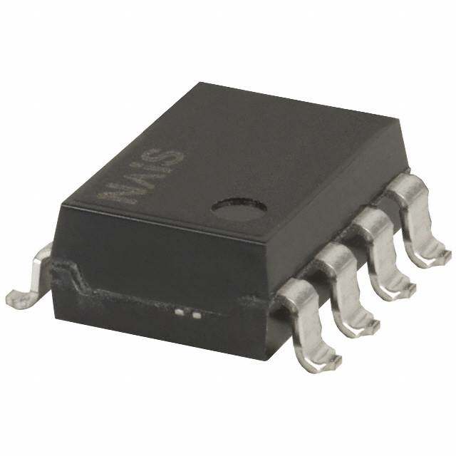
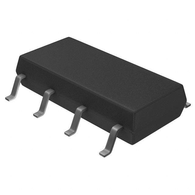
- 型号: AQY221R2TY
- 制造商: Panasonic Corporation
- 库位|库存: xxxx|xxxx
- 要求:
| 数量阶梯 | 香港交货 | 国内含税 |
| +xxxx | $xxxx | ¥xxxx |
查看当月历史价格
查看今年历史价格
AQY221R2TY产品简介:
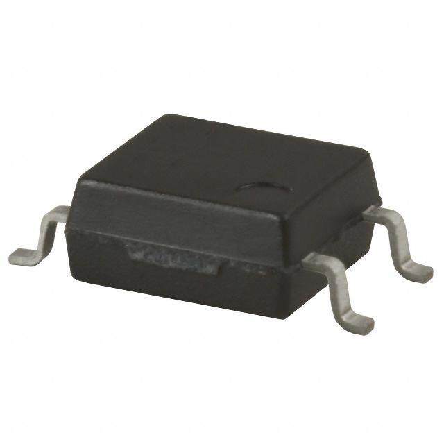
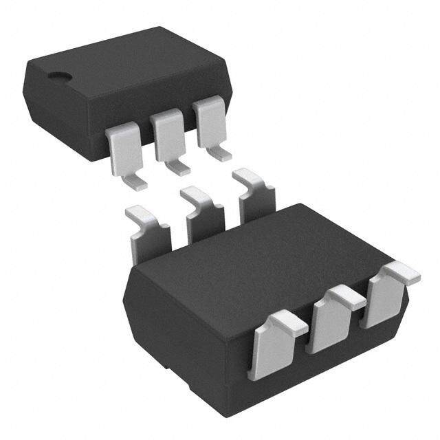
ICGOO电子元器件商城为您提供AQY221R2TY由Panasonic Corporation设计生产,在icgoo商城现货销售,并且可以通过原厂、代理商等渠道进行代购。 AQY221R2TY价格参考。Panasonic CorporationAQY221R2TY封装/规格:固态继电器, 固体继电器 继电器 SPST-NO(1 Form A) 4-SMD(0.071",1.80mm)。您可以下载AQY221R2TY参考资料、Datasheet数据手册功能说明书,资料中有AQY221R2TY 详细功能的应用电路图电压和使用方法及教程。
| 参数 | 数值 |
| 产品目录 | |
| 描述 | RELAY SSR RF SPST 40V 4-VSSOP固态继电器-PCB安装 RF VSSOP 1FORMA CXR10 |
| 产品分类 | |
| 品牌 | Panasonic Electric Works |
| 产品手册 | |
| 产品图片 |
|
| rohs | 符合RoHS无铅 / 符合限制有害物质指令(RoHS)规范要求 |
| 产品系列 | 固态继电器,固态继电器-PCB安装,Panasonic Industrial Devices AQY221R2TYPhotoMOS™ AQY2 |
| 数据手册 | |
| 产品型号 | AQY221R2TY |
| 产品 | Telecommunication Relays |
| 产品种类 | 固态继电器-PCB安装 |
| 产品类型 | PCB Mount |
| 供应商器件封装 | 4-VSSOP |
| 其它名称 | 255-3112-6 |
| 其它有关文件 | |
| 包装 | Digi-Reel® |
| 商标 | Panasonic Industrial Devices |
| 安装类型 | 表面贴装 |
| 安装风格 | SMD/SMT |
| 导通电阻 | 1.25 欧姆 |
| 导通电阻—最大值 | 0.8 Ohms |
| 封装 | Reel |
| 封装/外壳 | 4-SMD(0.087",2.20mm) |
| 封装/箱体 | SOP-4 |
| 工厂包装数量 | 1000 |
| 应用说明 | |
| 最大工作温度 | + 85 C |
| 最小工作温度 | - 40 C |
| 标准包装 | 1 |
| 特色产品 | http://www.digikey.com/cn/zh/ph/Panasonic/PhotoMOS.html |
| 电压-负载 | 0 ~ 40 V |
| 电压-输入 | 1.14VDC |
| 电路 | SPST-NO(1 A 形) |
| 端子类型 | SMD(SMT)接片 |
| 端接类型 | Gull Wing Lead |
| 继电器类型 | |
| 触点形式 | SPST (1 Form A) |
| 负载电压额定值 | 40 V |
| 负载电流 | 250mA |
| 负载电流额定值 | 250 mA |
| 输入转输出绝缘方法 | Optocoupler |
| 输出类型 | AC,DC(RF) |
| 输出设备 | MOSFET |
PDF Datasheet 数据手册内容提取
Smallest VSSOP package in its class × RF VSSOP 1 Form A C R10 4.6 mm2 mounting area/ 40 V load voltage (AQY221R2T) FEATURES New 1. VSSOP type with further reduction in mounting area .21.194 4.6 mm2 mounting area achieved. Approx 29% less than previous product (SON type). 2.2 2.1 .087 .083 Contributes to the miniaturization of instruments and higher density mounting. mm inch + 1 4 100% 44% 22% 16% – 2 3 SOP 4pin SSOP SON VSSOP 2. Low on resistance (R type) available Compliance with RoHS Directive Variation possible through combinations of output capacitance and On resistance. For more information, please contact our sales office in your area. 3. Low on resistance and low output capacitance available at C×R10 [Output capacitance: 14 pF (typical), On resistance: 0.8Ω (typical)] TYPICAL APPLICATIONS 1. Measuring and testing equipment IC tester, Probe card, Board tester and other testing equipment 2. Telecommunication equipment *Does not support automotive applications. TYPES Output rating*1 Part No. (Tape and reel packing style)*2 Packing quantity in Type Load voltage Load current Picked from the 1 and 4-pin side Picked from the 2 and 3-pin side the tape and reel AC/DC Low on resistance (R type) 40 V 250 mA AQY221R2TY AQY221R2TW 1,000 pcs. type Notes:*1 Indicate the peak AC and DC values. *2 Only tape and reel package is available. For space reasons, only “1R2” is marked on the product as the part number. RATING 1. Absolute maximum ratings (Ambient temperature: 25°C 77°F) Item Symbol AQY221R2T Remarks LED forward current IF 50 mA LED reverse voltage VR 5 V Input side Peak forward current IFP 1 A f = 100 Hz, Duty factor = 0.1% Power dissipation Pin 75 mW Load voltage (peak AC) VL 40 V Continuous load current IL 0.25 A Peak AC, DC Output side Peak load current Ipeak 0.75 A 100 ms (1shot), VL = DC Power dissipation Pout 250 mW Total power dissipation PT 300 mW I/O isolation voltage Viso 200 V AC Operating temperature Topr –40°C to +85°C –40°F to +185°F Non-condensing at low temperatures Storage temperature Tstg –40°C to +100°C –40°F to +212°F panasonic-electric-works.net/ac ASCTB1E 201105-T
× RF VSSOP 1 Form A C R10 (AQY221R2T) 2. Electrical characteristics (Ambient temperature: 25°C 77°F) Item Symbol AQY221R2T Condition Typical 0.5 mA LED operate current IFon IL = Max. Maximum 3 mA Minimum 0.1 mA Input LED turn off current IFoff IL = Max. Typical 0.4 mA Typical 1.14 V LED dropout voltage VF IF = 5 mA Maximum 1.5 V Typical 0.8 Ω On resistance Maximum Ron 1.25 Ω IF = 5 mA, IL = Max. Typical 14 pF Output Output capacitance Cout IF = 0 mA, f = 1 MHz, VB = 0 V Maximum 18 pF Typical 0.02 nA Off state leakage current ILeak IF = 0 mA, VL = Max. Maximum 10 nA Typical 0.1 ms Turn on time* Ton IF = 5 mA, VL = 10 V, RL = 40 Ω Maximum 0.5 ms Tcrhaanrsafcetre ristics Turn off time* MTayxpimicaulm Toff 00.0.26 mmss IF = 5 mA, VL = 10 V, RL = 40 Ω Typical 0.4 pF I/O capacitance Ciso f = 1 MHz, VB = 0 V Maximum 1.5 pF Note:Please refer to the “Schematic and Wiring Diagrams” for connection method. *Turn on/Turn off time Input 90% 10% Output Ton Toff RECOMMENDED OPERATING CONDITIONS Please obey the following conditions to ensure proper this device operation and resetting. Item Symbol Recommended value Unit Input LED current IF 5 mA REFERENCE DATA 1. Load current vs. ambient temperature 2. Load current vs. Load voltage characteristics 3. On resistance vs. ambient temperature characteristics Ambient temperature: 25°C 77°F characteristics Allowable ambient temperature:–40°C to +85°C Measured portion: between terminals 3 and 4 –40°F to +185°F LED current: 5 mA; Load voltage: 10V (DC); Continuous load current: 250 mA (DC) 400 400 5 4 Load current, mALoad current, mA 230000 Load current, mA 230000 ΩOn resistance, 23 100 100 1 0 0 0 -40 -20 0 20 40 60 8085100 0 10 20 30 40 50 -40 -20 0 20 40 60 8085 AAmmbbiieenntt tteemmppeerraattuurree,, °°CC Load voltage, V Ambient temperature, °C ASCTB1E 201105-T panasonic-electric-works.net/ac
× RF VSSOP 1 Form A C R10 (AQY221R2T) 4. Turn on time vs. ambient temperature 5. Turn off time vs. ambient temperature 6. LED operate current vs. ambient characteristics characteristics temperature characteristics Measured portion: between terminals 3 and 4 Measured portion: between terminals 3 and 4 Measured portion: between terminals 3 and 4 LED current: 5 mA; Load voltage: 10V (DC); LED current: 5 mA; Load voltage: 10V (DC); Load voltage: 10V (DC); Continuous load current: 250 mA (DC) Continuous load current: 250 mA (DC) Continuous load current: 250 mA (DC) 0.5 0.3 5 A Turn on time, ms 000...423 Turn off time, ms00.0.12.525 D operate current, m 423 0.1 E L 0.1 1 0.05 0 0 0 -40 -20 0 20 40 60 8085 -40 -20 0 20 40 60 8085 -40 -20 0 20 40 60 8085 Ambient temperature, °C Ambient temperature, °C Ambient temperature, °C 7. LED turn off current vs. ambient temperature 8. LED dropout voltage vs. ambient 9. Current vs. voltage characteristics of output characteristics temperature characteristics at MOS portion Measured portion: between terminals 3 and 4 LED current: 5 to 50 mA Measured portion: between terminals 3 and 4 Load voltage: 10V (DC); Ambient temperature: 25°C 77°F Continuous load current: 250 mA (DC) 5 1.5 300 A m LED turn off current, mA 423 LED dropout voltage, V 1111....4123 53210000mmmmAAAA -2 -1.5 -1 -Current, 0.5120000-1000.5 Vo1ltage1,. 5V 2 5mA 1 1 -200 0 0.9 -300 -40 -20 0 20 40 60 8085 -40 -20 0 20 40 60 8085 Ambient temperature, °C Ambient temperature, °C 10. Off state leakage current vs. load voltage 11. Turn on time vs. LED forward current 12. Turn off time vs. LED forward current characteristics characteristics characteristics Measured portion: between terminals 3 and 4 Measured portion: between terminals 3 and 4 Measured portion: between terminals 3 and 4 Ambient temperature: 25°C 77°F Load voltage: 10V (DC); Continuous load current: Load voltage: 10V (DC); Continuous load current: 250 mA (DC); Ambient temperature: 25°C 77°F 250 mA (DC); Ambient temperature: 25°C 77°F 0.5 0.5 A 10-3 nt, 0.4 0.4 ate leakage curre 10-6 Turn on time, ms 00..23 Turn off time, ms 00..23 Off st 10-9 0.1 0.1 10-12 0 0 0 10 20 30 40 50 0 10 20 30 40 50 60 0 10 20 30 40 50 60 Load voltage, V LED forward current, mA LED forward current, mA 13. Output capacitance vs. applied voltage 14. Isolation vs. frequency characteristics 15. Insertion loss vs. frequency characteristics characteristics (50Ω impedance) (50Ω impedance) Measured portion: between terminals 3 and 4 Measured portion: between terminals 3 and 4 Measured portion: between terminals 3 and 4 Frequency: 1 MHz, 30m Vrms; Ambient temperature: Ambient temperature: 25°C 77°F Ambient temperature: 25°C 77°F 25°C 77°F 25 100 2 F utput capacitance, p 112050 Isolation, dB 468000 Insertion loss, dB 1.15 O 0.5 5 20 0 0 0 0 10 20 30 40 50 105 106 107 108 104 105 106 107 Applied voltage, V Frequency, Hz Frequency, Hz panasonic-electric-works.net/ac ASCTB1E 201105-T
× RF VSSOP 1 Form A C R10 (AQY221R2T) 16. On resistance distribution 17. Turn on time distribution 18. Turn off time distribution Measured portion: between terminals 3 and 4 Load voltage: 10V (DC) Load voltage: 10V (DC) Continuous load current: 250 mA (DC), n: 50pcs. Continuous load current: 250 mA (DC), n: 50pcs. Continuous load current: 250 mA (DC), n: 50pcs. Ambient temperature: 25°C 77°F Ambient temperature: 25°C 77°F Ambient temperature: 25°C 77°F 50 50 50 40 40 40 Quantity, n 30 Quantity, n 30 Quantity, n 30 20 20 20 10 10 10 0 0 0 0.5 0.6 0.7 0.8 0.9 1.0 0 0.04 0.08 0.12 0.16 0.2 0 0.02 0.04 0.06 0.08 0.1 On resistance, Ω Turn on time, ms Turn off time, ms 19. LED operate current distribution Load voltage: 10V (DC) Continuous load current: 250 mA (DC), n: 50pcs. Ambient temperature: 25°C 77°F 50 40 n ntity, 30 a u Q 20 10 0 0 0.2 0.4 0.6 0.8 1 LED operate current, mA DIMENSIONS (mm inch) The CAD data of the products with a CAD Data mark can be downloaded from: http://panasonic-electric-works.net/ac CAD Data External dimensions Recommended mounting pad (Top view) 2.10 0.70 4 .083 3 .028 1.75 0.85 .069 1.0.8701 1 Input: DC+ .033 2 Input: DC− 1.27 3 Output: AC/DC .050 1 2 4 Output: AC/DC Tolerance: ±0.1 ±.004 2.90 .114 0.40 0.20 0.20 .016 0.40 .008 .008 .016 (2.20) 1.27 (.087) .050 General tolerance: ±0.1 ±.004 SCHEMATIC AND WIRING DIAGRAMS E1: Power source at input side, IF: LED forward current, VL: Load voltage, IL: Load current Output Schematic Load Connection Wiring diagram configuration + 1 4 4 Load 1 4 E1 1 Form A AC/DC — IF IL VL (AC,DC) IL VL (AC,DC) − 2 3 3 2 3 Load ASCTB1E 201105-T panasonic-electric-works.net/ac
× RF VSSOP 1 Form A C R10 (AQY221R2T) PhotoMOS CAUTIONS FOR USE SAFETY WARNINGS • Do not use the product under conditions • Do not touch the recharging unit while • Check the connection diagrams in the that exceed the range of its the power is on. There is a danger of catalog and be sure to connect the specifications. It may cause overheating, electrical shock. Be sure to turn off the terminals correctly. Erroneous smoke, or fire. power when performing mounting, connections could lead to unexpected maintenance, or repair operations on the operating errors, overheating, or fire. device (including connecting parts such as the terminal board and socket). 1. Please refer to “PhotoMOS®” 2) A conductive metal sheet should be 2) Even if spike voltages generated at the catalog (latest version) for cautions placed over the work table. Measuring load are limited with a clamp diode if the for use and explanations of instruments and jigs should be grounded. circuit wires are long, spike voltages will terminology. 3) When using soldering irons, either use occur by inductance. Keep wires as short 2. Derated designs irons with low leakage current, or ground as possible to minimize inductance. Consideration of reliability is absolutely the tip of the soldering iron. (Use of low- 7. Ripple in the input power supply imperative for derated designs because voltage soldering irons is also If ripple is present in the input power of its importance to the working lifetime of recommended.) supply, observe the following: the product. 4) Devices and equipment used in 1) For LED operate current at Emin, Please be sure to derate sufficiently from assembly should also be grounded. maintain the value mentioned in the table the maximum rating of the device when 5) When packing printed circuit boards of “Recommended LED forward current designing a system. Be sure to conduct and equipment, avoid using high-polymer (IF).” real-life testing of the product; and, if materials such as foam styrene, plastic, 2) Keep the LED operate current at necessary, provide extra leeway against and other materials which carry an 50 mA or less at Emax. the maximum rating by taking sufficiently electrostatic charge. safety measures. 6) When storing or transporting devices, 3. Applying stress that exceeds the the environment should not be conducive absolute maximum rating to generating static electricity (for Emin. Emax. If the voltage or current value for any of instance, the humidity should be between 8. Soldering the terminals exceeds the absolute 45 and 60%), and devices should be • Example of recommended soldering maximum rating, internal elements will protected using conductive packing conditions deteriorate because of the excessive materials. (1) IR (Infrared reflow) soldering method voltage or current. In extreme cases, 5. Short across terminals wiring may melt, or silicon P/N junctions Do not short circuit between terminals T3 may be destroyed. when device is energized, since there is T2 Therefore, the circuit should be designed possibility of breaking of the internal IC. in such a way that the load never exceed 6. Output spike voltages T1 the absolute maximum ratings, even 1) If an inductive load generates spike momentarily. voltages which exceed the absolute 4. Deterioration and destruction maximum rating, the spike voltage must t1 t2 caused by discharge of static be limited. Typical circuits are shown electricity below. T1 = 150 to 180°C302 to 356°F T2 = 230°C446°F This phenomenon is generally called T3 = 245°C473°For less 1 4 t1 = 60 to 120 s or less static electricity destruction, and occurs t2 = 30 s or less when static electricity generated by (2) Soldering iron method various factors is discharged while the Load Tip temperature: 350 to 400°C 662 to device terminals are in contact, 2 3 752°F producing internal destruction of the Wattage: 30 to 60 W element. Add a clamp diode to the load Soldering time: within 3 s To prevent problems from static 1 4 (3) Others electricity, the following precautions and Check mounting conditions before using measures should be taken when using other soldering methods (VPS, hot-air, your device. 2 3 Load hot plate, laser, pulse heater, etc.) 1) Employees handling devices should wear anti-static clothing and should be Add a CR snubber circuit to the load grounded through protective resistance of 500 kΩ to 1 MΩ. panasonic-electric-works.net/ac ASCTB1E 201105-T
× RF VSSOP 1 Form A C R10 (AQY221R2T) 9. Notes for mounting 10. Cleaning •Cleanser used: Asahiklin AK-225 1) If many different packages are This product creates a light path by •Other: combined on a single substrate, then coupling with resin the LED of the Submerge in solvent in order to prevent lead temperature rise is highly dependent emitting element and the solar cell of the the PCB and elements from being on package size. For this reason, please receiving element. For this reason, contacted directly by the ultrasonic make sure that the temperature of the ultrasonic cleaning should be avoided as vibrations. terminal solder area of the PhotoMOS much as possible, because the product Note:Applies to unit area ultrasonic output for falls within the temperature conditions of differs from other molded resin products ultrasonic baths. item “8. Soldering” before mounting. that contain discrete elements (MOS 2) If the mounting conditions exceed the transistors and bipolar transistors, etc.). recommended solder conditions in item We recommend cleaning with an organic 8, resin strength will fall and the solvent. If you cannot avoid using nonconformity of the heat expansion ultrasonic cleansing, please ensure that coefficient of each constituent material the following conditions are met, and will increase markedly, possibly causing check beforehand for defects. cracks in the package, severed bonding •Frequency: 27 to 29 kHz wires, and the like. For this reason, •Ultrasonic output: please inquire with us about whether this No greater than 0.25W/cm2 use is possible. •Cleaning time: No longer than 30 s 11. Device packaging format Tape and reel (Unit: mm inch) Tape dimensions Dimensions of paper tape reel 21±0.8 Tractor feed holes Direction of .827±.031 0.0.3185±±0.0.0052 1.0.5509 +−+− 00.00 .52 0d di2aia..7.±0.2 p.14ic5.k07i±n±0.0g.104 .10.6795±±.00.014 .106±.008 2±0.5 2.9±0.2 .079±.020 .114±.008 250±2 dia. 12.0±0.3 9.843±.079 dia. .472±.012 80±1 dia. 3.150±.039 dia. Device mounted 3.3±0.3 on tape 1±0.1 dia. 8±0.1 2±0.1 5.5±0.1 .130±.012 .039±.004 dia..315±.004 .079±.004.217±.004 13±0.5 dia. (1) When picked from 1 and 4-pin side: Part No. AQY❍❍❍TY (Shown above) .512±.020 dia..55114±.±015.59 2.0±70.59±.020 (2) When picked from 2 and 3-pin side: Part No. AQY❍❍❍TW 12. Transportation and storage moisture-proof bag containing silica gel discharge of static electricity”, and 1) Extreme vibration during transport will (within 3 months at the most). implement sufficient measures to control damage the device. Handle the outer and *When thermal stress is applied when static electricity. inner boxes with care. mounting with solder after the product 3) When installing the devices in the 2) Storage under extreme conditions will has absorbed moisture, the water will vicinity, please keep in mind that if the cause soldering degradation, external evaporate, swelling will occur, and the exposed frames of adjacent devices get appearance defects, and deterioration of inside of the package will become too close, a short between devices may the characteristics. The following storage stressed. Since this can lead to bulging occur. conditions are recommended: and cracking of the package surface, Part of frame on output side • Temperature: 0 to 45°C 32 to 113°F please be sure to be careful and follow • Humidity: Less than 70% R.H. the correct soldering conditions. • Atmosphere: No harmful gasses such 13. About the exposed terminals on as sulfurous acid gas, minimal dust. the sides of the package 3) PhotoMOS implemented in VSSOP As shown in the following figure, part of Part of frame on input side type are sensitive to moisture and come the input and output frames are exposed in sealed moisture-proof packages. on the sides of the package. Due to this, 14. Regarding close installations Observe the following cautions on please be keep in mind the cautions When this product is installed close to storage. listed below. other parts, the ambient temperature may • After the moisture-proof package is 1) Shorting the exposed terminals may rise due to heating of the internal element unsealed, take the devices out of storage cause deterioration of the insulation when power is applied. Be sure to use as soon as possible (within 1 month, less between the inputs and outputs, and may with a reduced load current after testing than 45°C 113°F/70% R.H.). damage the internal IC. under actual conditions, because the • If the devices are to be left in storage for 2) Since the exposed terminals are degree of temperature rise depends on a considerable period after the moisture- connected electrically to the internal the placement of the devices and proof package has been unsealed, it is element, please refer to the section “4. conditions of use. recommended to keep them in another Deterioration and destruction caused by ASCTB1E 201105-T panasonic-electric-works.net/ac
Mouser Electronics Authorized Distributor Click to View Pricing, Inventory, Delivery & Lifecycle Information: P anasonic: AQY221R2TW AQY221R2TY
 Datasheet下载


