ICGOO在线商城 > 分立半导体产品 > 晶体管 - FET,MOSFET - 阵列 > APTM50HM75STG

 Datasheet下载
- 型号: APTM50HM75STG
- 制造商: American Microsemiconductor, Inc.
- 库位|库存: xxxx|xxxx
- 要求:
| 数量阶梯 | 香港交货 | 国内含税 |
| +xxxx | $xxxx | ¥xxxx |
查看当月历史价格
查看今年历史价格
APTM50HM75STG产品简介:
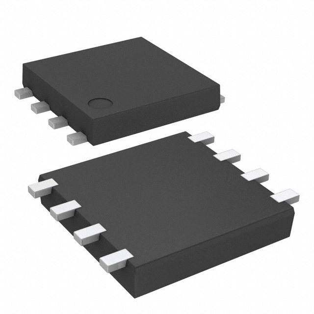
ICGOO电子元器件商城为您提供APTM50HM75STG由American Microsemiconductor, Inc.设计生产,在icgoo商城现货销售,并且可以通过原厂、代理商等渠道进行代购。 APTM50HM75STG价格参考¥889.56-¥1100.05。American Microsemiconductor, Inc.APTM50HM75STG封装/规格:晶体管 - FET,MOSFET - 阵列, 4 个 N 通道(H 桥) Mosfet 阵列 500V 46A 357W 底座安装 SP4。您可以下载APTM50HM75STG参考资料、Datasheet数据手册功能说明书,资料中有APTM50HM75STG 详细功能的应用电路图电压和使用方法及教程。
APTM50HM75STG 是 Microsemi Corporation(现为 Microchip Technology 旗下品牌)生产的一款 MOSFET 阵列器件,属于功率半导体器件。其主要应用场景包括:

1. 电源管理系统:适用于高效率、高功率密度的电源转换系统,如DC-DC转换器、AC-DC电源模块,尤其在需要多路输出或并联工作的场合。

2. 电机驱动:用于工业自动化设备、伺服电机驱动器及电动汽车中的电机控制系统,提供高效、可靠的开关性能。

3. 工业控制设备:如PLC(可编程逻辑控制器)、工业电源、UPS(不间断电源)等,满足高可靠性和稳定性要求。

4. 新能源系统:包括太阳能逆变器和储能系统中的功率转换部分,支持高电压和大电流工作环境。

5. 汽车电子:适用于车载充电系统、电池管理系统(BMS)以及48V轻混系统中,具备良好的热稳定性和抗干扰能力。

该器件采用高集成度设计,有助于减少外围电路复杂度,提高系统效率和可靠性,适合高功率密度和空间受限的应用场景。
| 参数 | 数值 |
| 产品目录 | |
| 描述 | MOSFET MOD FULL BRDG SER/PAR SP4 |
| 产品分类 | FET - 模块 |
| FET功能 | 标准 |
| FET类型 | 4 个 N 通道(H 桥) |
| 品牌 | Microsemi Power Products Group |
| 数据手册 | http://www2.microsemi.com/document-portal/doc_download/8195-aptm50hm75stg-rev4-pdfhttp://www2.microsemi.com/document-portal/doc_download/14813-power-products-group-ppg-catalog |
| 产品图片 |
|
| 产品型号 | APTM50HM75STG |
| rohs | 无铅 / 符合限制有害物质指令(RoHS)规范要求 |
| 产品系列 | - |
| 不同Id时的Vgs(th)(最大值) | 5V @ 2.5mA |
| 不同Vds时的输入电容(Ciss) | 5600pF @ 25V |
| 不同Vgs时的栅极电荷(Qg) | 123nC @ 10V |
| 不同 Id、Vgs时的 RdsOn(最大值) | 90 毫欧 @ 23A,10V |
| 产品目录页面 | |
| 供应商器件封装 | SP4 |
| 功率-最大值 | 357W |
| 包装 | 散装 |
| 安装类型 | 底座安装 |
| 封装/外壳 | SP4 |
| 标准包装 | 1 |
| 漏源极电压(Vdss) | 500V |
| 电流-连续漏极(Id)(25°C时) | 46A |


- 商务部:美国ITC正式对集成电路等产品启动337调查
- 曝三星4nm工艺存在良率问题 高通将骁龙8 Gen1或转产台积电
- 太阳诱电将投资9.5亿元在常州建新厂生产MLCC 预计2023年完工
- 英特尔发布欧洲新工厂建设计划 深化IDM 2.0 战略
- 台积电先进制程称霸业界 有大客户加持明年业绩稳了
- 达到5530亿美元!SIA预计今年全球半导体销售额将创下新高
- 英特尔拟将自动驾驶子公司Mobileye上市 估值或超500亿美元
- 三星加码芯片和SET,合并消费电子和移动部门,撤换高东真等 CEO
- 三星电子宣布重大人事变动 还合并消费电子和移动部门
- 海关总署:前11个月进口集成电路产品价值2.52万亿元 增长14.8%


PDF Datasheet 数据手册内容提取
APTM50HM75STG Full bridge V = 500V DSS Series & parallel diodes R = 75mΩ typ @ Tj = 25°C DSon I = 46A @ Tc = 25°C MOSFET Power Module D Application • Motor control VBUS • Switched Mode Power Supplies • Uninterruptible Power Supplies CR1A CR3A Q1 CR1B CR3B Q3 Features • Power MOS 7® MOSFETs G1 G3 S1 OUT1 OUT2 S3 - Low RDSon - Low input and Miller capacitance CR2A CR4A - Low gate charge CR2B CR4B - Avalanche energy rated Q2 Q4 - Very rugged G2 G4 • Kelvin source for easy drive S2 S4 • Very low stray inductance NTC1 0/VBUS NTC2 - Symmetrical design - Lead frames for power connections • Internal thermistor for temperature monitoring • High level of integration Benefits • Outstanding performance at high frequency operation • Direct mounting to heatsink (isolated package) • Low junction to case thermal resistance • Solderable terminals both for power and signal for easy PCB mounting • Low profile • RoHS compliant All ratings @ T = 25°C unless otherwise specified j Absolute maximum ratings Symbol Parameter Max ratings Unit V Drain - Source Breakdown Voltage 500 V DSS T = 25°C 46 I Continuous Drain Current c D T = 80°C 34 A c I Pulsed Drain current 184 DM 3 V Gate - Source Voltage ±30 V 1 GS 0 2 RDSon Drain - Source ON Resistance 90 mΩ er, b P Maximum Power Dissipation T = 25°C 357 W o D c ct O EIAARR ARevpaelatintcivhee Acuvrarleanntc (hree pEentietrivgey and non repetitive) 4560 mAJ ev 6 E Single Pulse Avalanche Energy 2500 R AS – G T These Devices are sensitive to Electrostatic Discharge. Proper Handling Procedures Should Be Followed.See application note S 5 APT0502 on www.microsemi.com 7 M 0H 5 M T P www.microsemi.com 1–7 A
APTM50HM75STG Electrical Characteristics Symbol Characteristic Test Conditions Min Typ Max Unit V = 0V,V = 500V T = 25°C 100 I Zero Gate Voltage Drain Current GS DS j µA DSS V = 0V,V = 400V T = 125°C 500 GS DS j R Drain – Source on Resistance V = 10V, I = 23A 75 90 mΩ DS(on) GS D V Gate Threshold Voltage V = V , I = 2.5mA 3 5 V GS(th) GS DS D I Gate – Source Leakage Current V = ±30 V, V = 0V ±100 nA GSS GS DS Dynamic Characteristics Symbol Characteristic Test Conditions Min Typ Max Unit Ciss Input Capacitance VGS = 0V 5600 C Output Capacitance V = 25V 1200 pF oss DS C Reverse Transfer Capacitance f = 1MHz 90 rss Q Total gate Charge 123 g V = 10V GS Q Gate – Source Charge V = 250V 33 nC gs Bus I = 46A Q Gate – Drain Charge D 65 gd Td(on) Turn-on Delay Time Inductive switching @ 125°C 18 T Rise Time VGS = 15V 35 r V = 333V ns T Turn-off Delay Time Bus 87 d(off) I = 46A D T Fall Time R = 5Ω 77 f G E Turn-on Switching Energy Inductive switching @ 25°C 755 on V = 15V, V = 333V µJ GS Bus E Turn-off Switching Energy I = 46A,R = 5Ω 726 off D G E Turn-on Switching Energy Inductive switching @ 125°C 1241 on V = 15V, V = 333V µJ GS Bus Eoff Turn-off Switching Energy ID = 46A, RG = 5Ω 846 R Junction to Case Thermal Resistance 0.35 °C/W thJC Series diode ratings and characteristics Symbol Characteristic Test Conditions Min Typ Max Unit V Maximum Peak Repetitive Reverse Voltage 600 V RRM I Maximum Reverse Leakage Current V =600V 250 µA RM R I DC Forward Current T = 70°C 30 A F c I = 30A 1.6 1.8 F V Diode Forward Voltage I = 60A 1.9 V F F I = 30A T = 125°C 1.4 F j T = 25°C 85 j Qtrr RReevveerrssee RReeccoovveerryy TCihmareg e VdIFi R/=d = t3 =40 0A200 V0A /µs TTjj == 12255°C°C 116300 nnCs ober, 2013 rr Tj = 125°C 700 Oct RthJC Junction to Case Thermal Resistance 1.2 °C/W 6 ev R – G T S 5 7 M 0H 5 M T P www.microsemi.com 2–7 A
APTM50HM75STG Parallel diode ratings and characteristics Symbol Characteristic Test Conditions Min Typ Max Unit V Maximum Peak Repetitive Reverse Voltage 600 V RRM I Maximum Reverse Leakage Current V = 600V 250 µA RM R I DC Forward Current T = 70°C 30 A F c I = 30A 1.6 1.8 F V Diode Forward Voltage I = 60A 1.9 V F F I = 30A T = 125°C 1.4 F j T = 25°C 85 j t Reverse Recovery Time ns rr I = 30A F T = 125°C 160 V = 400V j R Q Reverse Recovery Charge di/dt = 200A/µs Tj = 25°C 130 nC rr T = 125°C 700 j R Junction to Case Thermal Resistance 1.2 °C/W thJC Thermal and package characteristics Symbol Characteristic Min Max Unit V RMS Isolation Voltage, any terminal to case t =1 min, 50/60Hz 4000 V ISOL T Operating junction temperature range -40 150 J T Recommended junction temperature under switching conditions -40 Tmax -25 JOP J °C T Storage Temperature Range -40 125 STG T Operating Case Temperature -40 100 C Torque Mounting torque To heatsink M5 2.5 4.7 N.m Wt Package Weight 160 g Temperature sensor NTC (see application note APT0406 on www.microsemi.com). Symbol Characteristic Min Typ Max Unit R Resistance @ 25°C 50 kΩ 25 ∆R /R 5 % 25 25 B T = 298.15 K 3952 K 25/85 25 ∆B/B T =100°C 4 % C R R = 25 T: Thermistor temperature T exp⎢⎢⎣⎡B25/85⎜⎜⎝⎛T125 −T1⎟⎟⎠⎞⎥⎥⎦⎤ RT: Thermistor value at T SP4 Package outline (dimensions in mm) 3 1 0 2 er, b o ct O 6 v e R – G T S 5 See application note APT0501 - Mounting Instructions for SP4 Power Modules on www.microsemi.com M7 0H 5 M T P www.microsemi.com 3–7 A
APTM50HM75STG Typical Performance Curve Maximum Effective Transient Thermal Impedance, Junction to Case vs Pulse Duration 0.4 W) 0.35 0.9 C/ ° 0.3 e ( 0.7 c n 0.25 a d 0.5 e 0.2 p m al I 0.15 0.3 m r 0.1 e 0.1 h T 0.05 Single Pulse 0.05 0 0.00001 0.0001 0.001 0.01 0.1 1 10 rectangular Pulse Duration (Seconds) Low Voltage Output Characteristics Transfert Characteristics 180 120 160 VDS> ID(on)xRDS(on)MAX 8V 100 250µs pulse test @ < 0.5 duty cycle A) 140 VGS=10&15V A) nt ( 120 7.5V nt ( 80 Curre 100 7V Curre 60 Drain 6800 6.5V Drain 40 TJ=25°C I, D 40 6V I, D 20 20 5.5V TJ=125°C 0 0 0 5 10 15 20 25 0 1 2 3 4 5 6 7 8 V , Drain to Source Voltage (V) V , Gate to Source Voltage (V) DS GS RDS(on) vs Drain Current DC Drain Current vs Case Temperature e 1.20 c 50 n Normalized to a N Resist 11..1105 VGS=10V @ 23A VGS=10V rrent (A) 40 urce O 1.05 VGS=20V ain Cu 30 o So 1.00 C Dr 20 ain t 0.95 I, DD 10 r D on) 0.90 0 013 R(DS 0 20 40 60 80 100 25 50 75 100 125 150 er, 2 ID, Drain Current (A) TC, Case Temperature (°C) ctob O 6 v e R – G T S 5 7 M 0H 5 M T P www.microsemi.com 4–7 A
APTM50HM75STG Breakdown Voltage vs Temperature ON resistance vs Temperature e n 1.2 nc 2.5 dow sista VIDG=S2=31A0V Source BreakNormalized) 1.1 Source ON remalized) 12..50 o e ( 1.0 o or Drain tVoltag Drain t(N 1.0 , SS 0.9 n), 0.5 BVD 25 50 75 100 125 150 (oS 25 50 75 100 125 150 D TJ, Junction Temperature (°C) R TJ, Junction Temperature (°C) Threshold Voltage vs Temperature Maximum Safe Operating Area 1.1 1000 e ag 1.0 A) shold Voltalized) 0.9 n Current ( 100 limliimtedit ebdy bRyD RSoDnSon 100µs H), Thre(Norm 00..78 I, DraiD 10 STiJn=g15le0 °pCulse 1ms T T =25°C (S C 10ms G V 0.6 1 25 50 75 100 125 150 1 10 100 1000 T , Case Temperature (°C) V , Drain to Source Voltage (V) C DS Capacitance vs Drain to Source Voltage Gate Charge vs Gate to Source Voltage 100000 14 nce (pF)10000 CCoissss e Voltage (V) 11028 ITDJ==4265A°C VDS=250VVDS=1V0D0SV=400V apacita 1000 o Sourc 6 C, C 100 Crss ate t 4 G 2 , S G 10 V 0 0 10 20 30 40 50 0 20 40 60 80 100 120 140 160 13 0 VDS, Drain to Source Voltage (V) Gate Charge (nC) er, 2 b o ct O 6 v e R – G T S 5 7 M 0H 5 M T P www.microsemi.com 5–7 A
APTM50HM75STG Delay Times vs Current Rise and Fall times vs Current 100 120 td(off) VDS=333V 80 100 RTJG==152Ω5°C tf s) L=100µH nd t(nd(off) 4600 VRTL=JDG=S1=1=05230Ω53µ3H°VC and t(ns)f 6800 ad(on) td(on) tr 40 tr t 20 20 0 0 10 20 30 40 50 60 70 10 20 30 40 50 60 70 ID, Drain Current (A) ID, Drain Current (A) Switching Energy vs Current Switching Energy vs Gate Resistance 2.5 4 Switching Energy (mJ) 01..5512 VRTL=JDG=S1=1=05230Ω53µ3H°VC EoEnoff Switching Energy (mJ) 0123....1235555 VITLD=JD==S141=06230A53µ3H°VCEoff Eon 0 0 10 20 30 40 50 60 70 0 10 20 30 40 50 I , Drain Current (A) Gate Resistance (Ohms) D Operating Frequency vs Drain Current Source to Drain Diode Forward Voltage 1000 400 A) 350 ZVS VDD=S5=03%33V ent ( y (kHz) 235000 ZCS RTTJCG===17525Ω5°°CC ain Curr 100 TJ=150°C nc 200 Dr que 150 rse 10 e e Fr 100 ev T =25°C 50 swhitacrhdi ng , RDR J I 0 1 10 15 20 25 30 35 40 0.2 0.4 0.6 0.8 1 1.2 1.4 1.6 1.8 3 1 0 ID, Drain Current (A) VSD, Source to Drain Voltage (V) er, 2 b o ct 6 O v e R – G T S 5 7 M 0H 5 M T P www.microsemi.com 6–7 A
APTM50HM75STG DISCLAIMER The information contained in the document (unless it is publicly available on the Web without access restrictions) is PROPRIETARY AND CONFIDENTIAL information of Microsemi and cannot be copied, published, uploaded, posted, transmitted, distributed or disclosed or used without the express duly signed written consent of Microsemi. If the recipient of this document has entered into a disclosure agreement with Microsemi, then the terms of such Agreement will also apply. This document and the information contained herein may not be modified, by any person other than authorized personnel of Microsemi. No license under any patent, copyright, trade secret or other intellectual property right is granted to or conferred upon you by disclosure or delivery of the information, either expressly, by implication, inducement, estoppels or otherwise. Any license under such intellectual property rights must be approved by Microsemi in writing signed by an officer of Microsemi. Microsemi reserves the right to change the configuration, functionality and performance of its products at anytime without any notice. This product has been subject to limited testing and should not be used in conjunction with life- support or other mission-critical equipment or applications. Microsemi assumes no liability whatsoever, and Microsemi disclaims any express or implied warranty, relating to sale and/or use of Microsemi products including liability or warranties relating to fitness for a particular purpose, merchantability, or infringement of any patent, copyright or other intellectual property right. Any performance specifications believed to be reliable but are not verified and customer or user must conduct and complete all performance and other testing of this product as well as any user or customers final application. User or customer shall not rely on any data and performance specifications or parameters provided by Microsemi. It is the customer’s and user’s responsibility to independently determine suitability of any Microsemi product and to test and verify the same. The information contained herein is provided “AS IS, WHERE IS” and with all faults, and the entire risk associated with such information is entirely with the User. Microsemi specifically disclaims any liability of any kind including for consequential, incidental and punitive damages as well as lost profit. The product is subject to other terms and conditions which can be located on the web at http://www.microsemi.com/legal/tnc.asp Life Support Application Seller's Products are not designed, intended, or authorized for use as components in systems intended for space, aviation, surgical implant into the body, in other applications intended to support or sustain life, or for any other application in which the failure of the Seller's Product could create a situation where personal injury, death or property damage or loss may occur (collectively "Life Support Applications"). Buyer agrees not to use Products in any Life Support Applications and to the extent it does it shall conduct extensive testing of the Product in such applications and further agrees to indemnify and hold Seller, and its officers, employees, subsidiaries, affiliates, agents, sales representatives and distributors harmless against all claims, costs, damages and expenses, and attorneys' fees and costs arising, directly or directly, out of any claims of personal injury, death, damage or otherwise associated with the use of the goods in Life Support Applications, even if such claim includes allegations that Seller was negligent regarding the design or manufacture of the goods. Buyer must notify Seller in writing before using Seller’s Products in Life Support Applications. Seller will study with Buyer alternative solutions to meet Buyer application specification based on Sellers sales conditions applicable for the new proposed specific part. 3 1 0 2 er, b o ct O 6 v e R – G T S 5 7 M 0H 5 M T P www.microsemi.com 7–7 A
Mouser Electronics Authorized Distributor Click to View Pricing, Inventory, Delivery & Lifecycle Information: M icrosemi: APTM50HM75STG