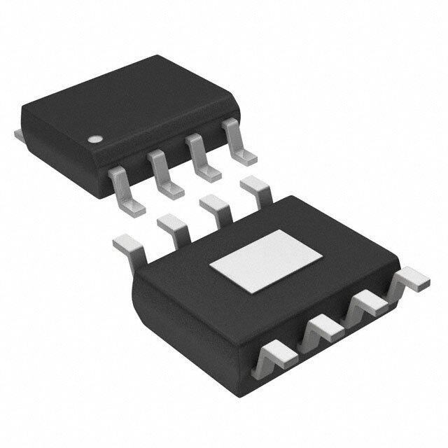
ICGOO在线商城 > AP6015-25M10G-13
- 型号: AP6015-25M10G-13
- 制造商: Diodes Inc.
- 库位|库存: xxxx|xxxx
- 要求:
| 数量阶梯 | 香港交货 | 国内含税 |
| +xxxx | $xxxx | ¥xxxx |
查看当月历史价格
查看今年历史价格
AP6015-25M10G-13产品简介:
ICGOO电子元器件商城为您提供AP6015-25M10G-13由Diodes Inc.设计生产,在icgoo商城现货销售,并且可以通过原厂、代理商等渠道进行代购。 提供AP6015-25M10G-13价格参考以及Diodes Inc.AP6015-25M10G-13封装/规格参数等产品信息。 你可以下载AP6015-25M10G-13参考资料、Datasheet数据手册功能说明书, 资料中有AP6015-25M10G-13详细功能的应用电路图电压和使用方法及教程。
| 参数 | 数值 |
| 产品目录 | 集成电路 (IC)半导体 |
| 描述 | IC REG BCK SYNC 2.5V 0.8A 10MSOP稳压器—开关式稳压器 1MHz 0.8A 2.5V-5.5V |
| 产品分类 | |
| 品牌 | Diodes Incorporated |
| 产品手册 | |
| 产品图片 |
|
| rohs | 符合RoHS无铅 / 符合限制有害物质指令(RoHS)规范要求 |
| 产品系列 | 电源管理 IC,稳压器—开关式稳压器,Diodes Incorporated AP6015-25M10G-13- |
| 数据手册 | |
| 产品型号 | AP6015-25M10G-13 |
| PWM类型 | 电流模式 |
| RoHS指令信息 | http://diodes.com/download/4349 |
| 产品目录页面 | |
| 产品种类 | 稳压器—开关式稳压器 |
| 供应商器件封装 | 10-MSOP |
| 其它名称 | AP6015-25M10GDICT |
| 包装 | 剪切带 (CT) |
| 同步整流器 | 是 |
| 商标 | Diodes Incorporated |
| 安装类型 | 表面贴装 |
| 安装风格 | SMD/SMT |
| 封装 | Reel |
| 封装/外壳 | 10-TFSOP,10-MSOP(0.118",3.00mm 宽) |
| 封装/箱体 | MSOP-10 |
| 工作温度 | -40°C ~ 85°C |
| 工厂包装数量 | 2500 |
| 开关频率 | 1000 kHz |
| 最大工作温度 | + 85 C |
| 最大输入电压 | 5.5 V |
| 最小工作温度 | - 40 C |
| 标准包装 | 1 |
| 电压-输入 | 2.5 V ~ 5.5 V |
| 电压-输出 | 2.5V |
| 电流-输出 | 800mA |
| 类型 | Switching Regulator |
| 系列 | AP6015 |
| 输出数 | 1 |
| 输出电压 | 2.5 V |
| 输出电流 | 800 mA |
| 输出端数量 | 1 Output |
| 输出类型 | 固定 |
| 频率-开关 | 1MHz |





- 商务部:美国ITC正式对集成电路等产品启动337调查
- 曝三星4nm工艺存在良率问题 高通将骁龙8 Gen1或转产台积电
- 太阳诱电将投资9.5亿元在常州建新厂生产MLCC 预计2023年完工
- 英特尔发布欧洲新工厂建设计划 深化IDM 2.0 战略
- 台积电先进制程称霸业界 有大客户加持明年业绩稳了
- 达到5530亿美元!SIA预计今年全球半导体销售额将创下新高
- 英特尔拟将自动驾驶子公司Mobileye上市 估值或超500亿美元
- 三星加码芯片和SET,合并消费电子和移动部门,撤换高东真等 CEO
- 三星电子宣布重大人事变动 还合并消费电子和移动部门
- 海关总署:前11个月进口集成电路产品价值2.52万亿元 增长14.8%


PDF Datasheet 数据手册内容提取
NOT RECOMMENDED FOR NEW DESIGN USE AP3428 AP6015 High Efficiency Step-Down Low Power DC-DC Converter Features General Description High efficiency synchronous step-down converter with The AP6015 is the first device in a family of low-noise current greater than 94% mode synchronous step-down DC-DC converters. It is ideally Current Mode Operation for faster transient response suited for systems powered by either a 1-cell Li-ion battery or a 2- and better loop stabilization to 3-cell NiCd/ NiMH/ Alkaline battery. 2.5V to 5.5V operating input voltage range The AP6015 is a synchronous PWM converter with integrated Adjustable output voltage range from 0.8V to VIN N- and P-channel power MOSFET switches. Compared to the Fixed output voltage options: 1.8V, 2.5V and 3.3V asynchronous topology, synchronous rectification offers the Up to 800mA output current benefits of higher efficiency and reduced component count. The High efficiency over a wide range of load currents high operating frequency of 1MHz allows small inductor and PWM operation mode capacitor to be used. This results in small pcb area. During Internal soft-start function shut-down, the standby current drops to 1μA or less. The Typical quiescent current of 150μA AP6015 is available in the 10-pin MSOP package. It operates MSOP-10L: Available in “Green” Molding Compound over a free-air temperature range of -40oC to 85o C. (No Br, Sb) Lead Free Finish/ RoHS Compliant (Note 1) Applications Mobile Handsets PDAs, Ultra Mobile PCs Portable Media Players, Digital Still/Video Cameras USB-based DSL Modems LAN/WLAN/WPAN/WWAN Modules Ordering Information AP 6015 - XX M10 G - 13 Voltage Package Green Packing Blank : Adj M10 : MSOP-10L G : Green 13 : Tape & Reel 18 : 1.8V 25 : 2.5V 33 : 3.3V Package Packaging 13” Tape and Reel Device Code (Note 2) Quantity Part Number Suffix AP6015-XXM10G-13 M10 MSOP-10L 2500/Tape & Reel -13 Notes: 1. EU Directive 2002/95/EC (RoHS). All applicable RoHS exemptions applied, see EU Directive 2002/95/EC Annex Notes. 2. Pad layout as shown on Diodes Inc. suggested pad layout document AP02001, which can be found on our website at http://www.diodes.com/datasheets/ap02001.pdf. AP6015 Rev. 4-3 1 of 19 January 2018 www.diodes.com © Diodes Incorporated
AP6015 High Efficiency Step-Down Low Power DC-DC Converter Pin Assignment ( Top View ) PVCC 1 10 PGND VCC 2 9 LX GND 3 8 EN PG 4 7 NC FB/Vout 5 6 CC MSOP-10L Pin Descriptions Pin Name Pin NO. I/O Description PVCC 1 I Supply voltage input Supply bypass pin. A 1μF coupling capacitor should be connected as close VCC 2 as possible to this pin. GND 3 Ground Power good comparator output. A pull-up resistor should be connected PG 4 O between PG and V . O FB 5 I Feedback pin for the fixed output voltage option. CC 6 I Compensation pin NC 7 NC No connect EN 8 I Enable.Pin, H: Enable. L:shutdown LX 9 I/O Connect the inductor to this pin. PGND 10 Power ground AP6015 Rev. 4-3 2 of 19 January 2018 www.diodes.com © Diodes Incorporated
AP6015 High Efficiency Step-Down Low Power DC-DC Converter Block Diagram VCC CCCC PPGG ECNE UVLO SSSS TS Bias Open drain - Vref=0.8V ER-AMP + FFBB - PG_COM Current + Protection PVCC PVCC + Buffer LX PWM--COM BANDGAP Osc Vramp - GND PGND PGND Notes: 3. The adjustable output voltage version does not use the internal feedback resistor divider. The FB pin is directly connected to the error amplifier. Absolute Maximum Ratings Symbol Parameter Rating Unit ESD HBM Human Body Model ESD Protection 2.5 KV ESD MM Machine Model ESD Protection 300 V PVCC, VCC Supply Voltage -0.3 to +5.5 V Voltages on pins EN, CC, PG, FB, LX -0.3 to V +0.3 V IN T Maximum Junction Temperature Range +150 oC J(MAX) T Storage temperature range -65 to +150 oC ST T Operating Junction Temperature Range -40 to +125 oC OP Stresses beyond those listed under “absolute maximum ratings” may cause permanent damage to the device. These are stress ratings only and functional operation of the device at these or any other conditions beyond those indicated under “recommended operating conditions” is not implied. Exposure to absolute-maximum-rated conditions for extended periods ma affect device reliability. AP6015 Rev. 4-3 3 of 19 January 2018 www.diodes.com © Diodes Incorporated
AP6015 High Efficiency Step-Down Low Power DC-DC Converter Recommended Operating Conditions (TA :-40~85C) Symbol Parameter Rating Unit T Operating Ambient Temperature Range -40 to +85 oC A V Supply Voltage 2.0 to 5.5 V IN V Output voltage range for adjustable output voltage version 0.8 to V V O I L Inductor (see Note 4) 3.3 μH C Input capacitor (see Note 4) 10 μF i C Output capacitor (see Note 4) V ≥ 1.8V 10 μF o O Notes: 4. Refer to application section for further information. Electrical Characteristics (TA =25C) Over recommended operating free-air temperature range, VI=3.6V, VO=2.5V, IO=300mA, EN=VIN. (unless otherwise noted) Symbol Parameter Conditions Min Typ. Max Unit Supply current I = 0mA to 800mA 2.5 - 5.5 -20 to 85 oC O I = 0mA to 500mA 2 - 5.5 O V Input Voltage range V IN I = 0mA to 600mA 2.5 5.5 -40 to 85 oC O I = 0mA to 400mA 2 - - O Iccq Operating quiescent current I = 0mA - 150 - μA O I Standby current EN= GND - 0.1 1 μA STBY Enable V ≤ 3V 1.5 - - IN V EN high-level input voltage V IH V > 3V 2.5 - - IN V EN low-level input voltage - - 0.7 V IL I EN input leakage current EN= GND or V - 0.01 0.1 μA L IN V Under-voltage-lockout-threshold 1.2 1.6 1.95 V (UVLO) AP6015 Rev. 4-3 4 of 19 January 2018 www.diodes.com © Diodes Incorporated
AP6015 High Efficiency Step-Down Low Power DC-DC Converter Electrical Characteristics (Continued) Over recommended operating free-air temperature range, VI=3.6V, VO=2.5V, IO=300 mA, EN=VIN. (unless otherwise noted) Symbol Parameter Conditions Min Typ. Max Unit Power switch and current limit V=V =3.6V; I=200mA 200 280 410 P-channel MOSFET on-resistance I GS mΩ V=V =2V; I=200mA - 480 - I GS P-channel leakage current V =5.5V - - 1 μA R DS DS(on) V=V =3.6V; I =200mA 200 280 410 N-channel MOSFET on-resistance I GS O mΩ V=V =2V; I =200mA - 500 - I GS O N-channel leakage current V =5.5V - - 1 μA DS I P-channel current limit 2.5V≤V≤5.5V 1200 - 1600 mA (LIM) I Power good output (see Note 5) 88% 92% 94% Power good threshold Feedback voltage falling V V V V V (PG) O O O Power good hysteresis 2.5% V O V =0.8×V nominal; V PG output low voltage (FB) O - - 0.3 V OL I =10μA (sink) I PG output leakage current V =V nominal 0.01 1 μA LKG (FB) O Minimum supply voltage for valid 1.2 - - V power good signal Oscillator F Oscillator frequency 800 1000 1200 KHz S Output V Adjustable output voltage range 0.8 5.5 V O V Reference voltage 0.784 0.8 0.816 V REF AP6015-Adj V=2.5V to 5.5V; I -3% - 4% 0mA ≤ I ≤ 800mA AP6015-1.8V O 10mA ≤ I ≤ 800mA -3% - 3% O Fixed output V=2.7V to 5.5V; I -3% - 4% VO voltage AP6015-2.5V 0mA ≤ IO ≤ 800mA V (see Note 6) 10mA ≤ I ≤ 800mA -3% - 3% O V=3.6V to 5.5V; I -3% - 4% AP6015-3.3V 0mA ≤ I ≤ 800mA O 10mA ≤ I ≤ 800mA -3% - 3% O V= V +0.5V (min.2V) Line regulation I O 0.3 %/V to 6.0V; I =10mA O V=5.0V; Load regulation I 0.8 % I =10mA to 800mA O V=5V; V =3.3V; I =300mA η Efficiency I O O 94 % V=3.6V; V =2.5V; I =200mA I O O I =0mA, time from Start-up time O 0.4 1 4 ms active EN to V O Thermal Resistance θ MSOP-10L (Note 7) 161 oC/W JA Junction-to-Ambient Thermal Resistance θ MSOP-10L (Note 7) 39 oC/W JC Junction-to-Case Notes: 5. Power good is not valid for the first 100μs after EN goes high. Please refer to the application section for more information. 6. The output voltage accuracy includes line and load regulation over the full temperature range. 7. Test condition for MSOP-10L: Device mounted on 2oz copper, minimum recommended pad layout on top & bottom layer with thermal vias, double sided FR-4 PCB AP6015 Rev. 4-3 5 of 19 January 2018 www.diodes.com © Diodes Incorporated
AP6015 High Efficiency Step-Down Low Power DC-DC Converter Typical Application Circuit For best transient response we suggest that R , C and L1 values as below. CC CC R C L1-WURTH C1, C2 (MLCC) CC CC V < 3.0V, V < 2.5V 200KΩ 33PF 1.8µH 10µF IN OUT V 3.0V, V < 2.5V 68KΩ 100PF 1.8µH 10µF IN OUT V 3.0V, V 2.5V 82KΩ 100PF 3.3µH 10µF IN OUT (1) ADJ Output VI3.0 V to 5.5 V 1 PVCC LX 9 L1 V 2.5 V/800 mA O 100 Ohm 2 VCC FB 5 R3 680K AP6015 R1 8 4 EN PG Power Good C1 C2 10µF 10µF PGND 10 C3 R2 1µF GND CC 3 6 Rcc C CC 100pF R2: Suggest to be 39K~100K because of stability reasons. R V V (1 1) O REF R 2 Typical Application Circuit for Adjustable Output Voltage Option (2) FIXED Output Typical Application L1 V 5 V 1 PVCC LX 9 V 1.8/ 2.5/ 3.3V/ 800mA I O 100 Ohm 2 5 VCC FB R3 C1 AP6015 680K C2 10uF 8 EN PG 4 Power Good 10uF C3 1uF PGND 10 GND CC 3 6 Rcc C CC 100pF Standard 5 V to 1.8/ 2.5/ 3.3V/ 800mA Conversion; High Efficiency AP6015 Rev. 4-3 6 of 19 January 2018 www.diodes.com © Diodes Incorporated
AP6015 High Efficiency Step-Down Low Power DC-DC Converter Typical Operating Characteristics Input Voltage vs. Supply Current Supply Current vs. Temperature (Vcc=3.6V Vout=2.5V) 250 250 200 200 A) A) u u nt (150 nt ( 150 e e urr urr C C y 100 y 100 pl pl p p u u S S 50 50 Vout=0.8V Vout=1.8V 0 0 2 2.5 3 3.6 4 4.5 5 5.5 -40 -25 0 25 50 85 Input Voltage (V) Temperature (℃) Figure 1 Figure 2 Stand-by Current vs. Input Voltage Stand-by Current vs. Temperature (Vcc=3.6V) 0.1 1.2 1 0.08 A) A) u u nt ( 0.06 nt ( 0.8 e e rr rr u u 0.6 C C by 0.04 by d- d- 0.4 n n a a St 0.02 St 0.2 0 0 2 2.5 3 3.6 4 4.5 5 5.5 -40 -25 0 25 50 85 Input Voltage (V) Temperature (℃) Figure 3 Figure 4 AP6015 Rev. 4-3 7 of 19 January 2018 www.diodes.com © Diodes Incorporated
AP6015 High Efficiency Step-Down Low Power DC-DC Converter Typical Operating Characteristics (Continued) Line Regulation Load Regulation (Vout=2.5V Iout=10mA) (Vcc=5.0V Vout=2.5V) 2.55 2.55 2.54 2.54 2.53 2.53 V)2.52 V) 2.52 e ( e ( g2.51 g 2.51 a a olt 2.5 olt 2.5 V V ut 2.49 ut 2.49 p p ut2.48 ut 2.48 O O 2.47 2.47 2.46 2.46 2.45 2.45 3.0V 3.6 4 4.5 5 5.5 10 100 200 400 600 800 Input Voltage (V) Output Current (mA) Figure 5 Figure 6 Frequency vs. Temperature UVLO vs. Temperature (Vcc=3.6V Vout=2.5V) 1050 1.8 1000 1.72 z) H 950 ncy (K 900 LO (V)1.64 e V u U1.56 q e 850 r F 1.48 800 750 1.4 -40 -25 0 25 50 85 -40 -25 0 25 50 85 Temperature (℃) Temperature (℃) Figure 7 Figure 8 AP6015 Rev. 4-3 8 of 19 January 2018 www.diodes.com © Diodes Incorporated
AP6015 High Efficiency Step-Down Low Power DC-DC Converter Typical Operating Characteristics (Continued) Efficiency vs. Load Current Efficiency vs. Load Current (Vcc=3.6V Vout=1.8V) (Vcc=3.6V Vout=2.5V) 100 100 90 90 80 80 ) 70 70 % %) ncy ( 5600 ncy ( 5600 e e Effici 3400 Effici 3400 20 20 10 10 0 0 0 100 200 300 400 500 600 700 800 0 100 200 300 400 500 600 700 800 Load Current (mA) Load Current (mA) Figure 9 Figure 10 Efficiency vs. Load Current Efficiency vs. Load Current (Vcc=5.0V Vout=2.5V) (Vcc=5.0V Vout=3.3V) 100 100 90 90 80 80 70 70 %) %) y ( 60 y ( 60 c c n 50 n 50 e e Effici 40 Effici 40 30 30 20 20 10 10 0 0 0 100 200 300 400 500 600 700 800 0 100 200 300 400 500 600 700 800 Load Current (mA) Load Current (mA) Figure 11 Figure 12 AP6015 Rev. 4-3 9 of 19 January 2018 www.diodes.com © Diodes Incorporated
AP6015 High Efficiency Step-Down Low Power DC-DC Converter Typical Operating Characteristics (Continued) Dropout Voltage vs. Load Current Dropout Voltage vs. Load Current (Vout=2.5V) (Vout=3.3V) 400 400 350 350 V) 300 V) 300 m m ge ( 250 ge ( 250 a a olt 200 olt 200 V V ut 150 ut 150 o o p p o o r 100 r 100 D D 50 50 0 0 0 100 200 300 400 500 600 700 800 0 100 200 300 400 500 600 700 800 Load Current (mA) Load Current (mA) Figure 13 Figure 14 Output Ripple Output Ripple Figure 15 Figure 16 AP6015 Rev. 4-3 10 of 19 January 2018 www.diodes.com © Diodes Incorporated
AP6015 High Efficiency Step-Down Low Power DC-DC Converter Typical Operating Characteristics (Continued) Load Transient Response Load Transient Response Figure 17 Figure 18 Load Transient Response Load Transient Response Figure 19 Figure 20 AP6015 Rev. 4-3 11 of 19 January 2018 www.diodes.com © Diodes Incorporated
AP6015 High Efficiency Step-Down Low Power DC-DC Converter Application Information Enable (EN) When EN is on logic low, the AP6015 goes into shutdown mode. In shutdown, all other functions are turned off. The supply current is reduced to 1uA (Typ.). Soft Start As the enable pin goes high, the soft-start function generates an internal voltage ramp. This causes the start-up current to slowly raise preventing output voltage overshoot and high inrush currents. The soft-start duration is typical 1mSec. AP6015 START-UP TIME Under Voltage Lock Out (UVLO) The UVLO prevents the converter from turning on when the voltage on V is less than typically 1.6V. CC 3.6V Vcc 1.6V UVLO 0V 2.5V Vout 0V AP6015 Rev. 4-3 12 of 19 January 2018 www.diodes.com © Diodes Incorporated
AP6015 High Efficiency Step-Down Low Power DC-DC Converter Application Information (Continued) Power Good (PG) The PG comparator has an open drain output capable of sinking typically 10mA. The PG is only active when the AP6015 is enable (EN=high). When the AP6015 is disable (EN=low), the PG pin is high impedance. If the PG pin is connected to the output of the AP6015 with a pull-up resistor, no initial spike occurs and precautions have to be taken during start-up. The PG pin becomes active high when the output voltage exceeds typically 92% of its nominal value. Leave the PG pin unconnected when not used. PG Sink Current vs. ExteranI Voltage 25 ) 20 A m nt ( 15 e r r u C k 10 n Si G P 5 0 2 2.5 3 3.6 4 4.5 5 5.5 External Voltage (V) AP6015 Rev. 4-3 13 of 19 January 2018 www.diodes.com © Diodes Incorporated
AP6015 High Efficiency Step-Down Low Power DC-DC Converter Application Information (Continued) Inductor Selection In order to avoid saturation of the inductor, the inductor should be rated at least for the maximum output current plus the inductor ripple current which is calculated as: V 1( O ) V I I V CC I I L L O L f L(MAX) O(MAX) 2 Where: f= Switching frequency (1MHz typical) L = Inductor value △I = Peak-to-peak inductor ripple current L I (max) = Maximum inductor current L Vcc=3.6V Vout=2.5V f=1MHz L=3.3uH Vcc=3.6V Vout=2.5V f=1MHz L=1.8uH △I ≒230mA △I ≒360mA L L AP6015 Rev. 4-3 14 of 19 January 2018 www.diodes.com © Diodes Incorporated
AP6015 High Efficiency Step-Down Low Power DC-DC Converter Application Information (Continued) Input Capacitor Selection Though there is no special requirement for the ESR (Equivalent Series Resistance) of the input capacitor, due attention should be paid to the tolerance and temperature coefficient of the capacitor used. A 10uF or larger capacitance is required between the PVCC and the GND pins. The input capacitor should be placed as close as possible to the PVCC pin in order to achieve good overall system performance. Output Capacitor Selection Ripple at the voltage output pin is caused by the charge-and-discharge of the output capacitor. For the best performance, a low ESR output capacitor should be used. The equation below demonstrates how the size of the ripple can be calculated. V 1( O ) V 1 1 V V CC ( ESR) I ( ESR) O O L f 8C f L 8C f O O Where: △Vo= Output voltage ripple L = Inductor value f = Switching frequency (1MHz typical) △I = Peak-to-peak inductor ripple current L AP6015 Rev. 4-3 15 of 19 January 2018 www.diodes.com © Diodes Incorporated
AP6015 High Efficiency Step-Down Low Power DC-DC Converter Application Information (Continued) Layout Considerations A good board layout practice can significantly improve the stability of the application circuit and reduce the system noise. The feedback path must be as short as possible. The input capacitor and bypass capacitor must be placed close to the PVCC and the VCC pins for optimal performance. It is recommended that the ground planes for System Ground / Power Ground / Analog Ground are isolated from each others, while they should all be joined together at a common point. An example drawing of a circuit with good ground noise performance is shown below. L1 V 1 PVCC LX 9 V I O 100 Ohm 2 VCC FB 5 R3 680K AP6015 R1 8 EN PG 4 Power Good C1 C3 C2 10µF 1µF 10 uF 10 PGND R2 GND CC 3 6 Rcc C CC 100 pF The external inductor must be placed as close as possible to the switching node, i.e. the LX pin. The copper traces on the pcb, where high peak switching current may flow through, should be kept ‘wide’ and ‘short’. This results in low inductance and capacitance in the current path, hence ground shift problem is avoided and system stability stay within bound. AP6015 Rev. 4-3 16 of 19 January 2018 www.diodes.com © Diodes Incorporated
AP6015 High Efficiency Step-Down Low Power DC-DC Converter Marking Information ( Top View ) 10 9 8 7 6 A~Z : Green Logo Y W X Y : Year : 0~9 W : Week : A~Z : 1~26 week; Part Number 6015XX a~z : 27~52 week; z represents 52 and 53 week XX : 18 for 1.8V 25 for 2.5V 33 for 3.3V 1 2 3 4 5 Blank for ADJ MSOP-10L Package Information (All Dimensions in mm) (1) Package type: MSOP-10L 1 10x-0.30 5 0 0 3. 5. 2.95/ 4.8/ 4.4 8x-0.50 1 4 -1. x 0.1/0.2 0.21.79/50/.32.705 0.75/0.951.10Max. 10Land Pattern Re(Uconmit1:mmemnd)ation Seting plane 0.10 C 0.5Typ.05/0.15 C 0.25 "A" 0. Gauge plane 0.4/0.7 8° DETAIL "A" 0°/ AP6015 Rev. 4-3 17 of 19 January 2018 www.diodes.com © Diodes Incorporated
AP6015 High Efficiency Step-Down Low Power DC-DC Converter IMPORTANT NOTICE DIODES INCORPORATED MAKES NO WARRANTY OF ANY KIND, EXPRESS OR IMPLIED, WITH REGARDS TO THIS DOCUMENT, INCLUDING, BUT NOT LIMITED TO, THE IMPLIED WARRANTIES OF MERCHANTABILITY AND FITNESS FOR A PARTICULAR PURPOSE (AND THEIR EQUIVALENTS UNDER THE LAWS OF ANY JURISDICTION). Diodes Incorporated and its subsidiaries reserve the right to make modifications, enhancements, improvements, corrections or other changes without further notice to this document and any product described herein. Diodes Incorporated does not assume any liability arising out of the application or use of this document or any product described herein; neither does Diodes Incorporated convey any license under its patent or trademark rights, nor the rights of others. Any Customer or user of this document or products described herein in such applications shall assume all risks of such use and will agree to hold Diodes Incorporated and all the companies whose products are represented on Diodes Incorporated website, harmless against all damages. Diodes Incorporated does not warrant or accept any liability whatsoever in respect of any products purchased through unauthorized sales channel. Should Customers purchase or use Diodes Incorporated products for any unintended or unauthorized application, Customers shall indemnify and hold Diodes Incorporated and its representatives harmless against all claims, damages, expenses, and attorney fees arising out of, directly or indirectly, any claim of personal injury or death associated with such unintended or unauthorized application. Products described herein may be covered by one or more United States, international or foreign patents pending. Product names and markings noted herein may also be covered by one or more United States, international or foreign trademarks. This document is written in English but may be translated into multiple languages for reference. Only the English version of this document is the final and determinative format released by Diodes Incorporated. LIFE SUPPORT Diodes Incorporated products are specifically not authorized for use as critical components in life support devices or systems without the express written approval of the Chief Executive Officer of Diodes Incorporated. As used herein: A. Life support devices or systems are devices or systems which: 1. are intended to implant into the body, or AP6015 Rev. 4-3 18 of 19 January 2018 www.diodes.com © Diodes Incorporated
AP6015 High Efficiency Step-Down Low Power DC-DC Converter 2. support or sustain life and whose failure to perform when properly used in accordance with instructions for use provided in the labeling can be reasonably expected to result in significant injury to the user. B. A critical component is any component in a life support device or system whose failure to perform can be reasonably expected to cause the failure of the life support device or to affect its safety or effectiveness. Customers represent that they have all necessary expertise in the safety and regulatory ramifications of their life support devices or systems, and acknowledge and agree that they are solely responsible for all legal, regulatory and safety-related requirements concerning their products and any use of Diodes Incorporated products in such safety-critical, life support devices or systems, notwithstanding any devices- or systems-related information or support that may be provided by Diodes Incorporated. Further, Customers must fully indemnify Diodes Incorporated and its representatives against any damages arising out of the use of Diodes Incorporated products in such safety-critical, life support devices or systems. Copyright © 2018, Diodes Incorporated www.diodes.com AP6015 Rev. 4-3 19 of 19 January 2018 www.diodes.com © Diodes Incorporated

 Datasheet下载


