ICGOO在线商城 > 集成电路(IC) > PMIC - LED 驱动器 > AP3036BKTR-G1
 Datasheet下载
- 型号: AP3036BKTR-G1
- 制造商: Diodes Inc.
- 库位|库存: xxxx|xxxx
- 要求:
| 数量阶梯 | 香港交货 | 国内含税 |
| +xxxx | $xxxx | ¥xxxx |
查看当月历史价格
查看今年历史价格
AP3036BKTR-G1产品简介:
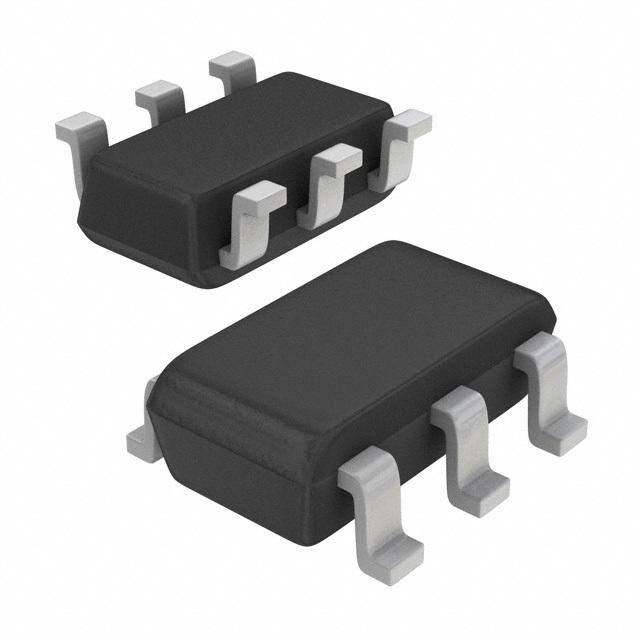
ICGOO电子元器件商城为您提供AP3036BKTR-G1由Diodes Inc.设计生产,在icgoo商城现货销售,并且可以通过原厂、代理商等渠道进行代购。 AP3036BKTR-G1价格参考¥1.19-¥1.19。Diodes Inc.AP3036BKTR-G1封装/规格:PMIC - LED 驱动器, LED 驱动器 IC 1 输出 DC DC 稳压器 升压 PWM 调光 550mA(开关) SOT-23-6。您可以下载AP3036BKTR-G1参考资料、Datasheet数据手册功能说明书,资料中有AP3036BKTR-G1 详细功能的应用电路图电压和使用方法及教程。
AP3036BKTR-G1 是由 Diodes Incorporated 生产的一款 PMIC(电源管理集成电路)- LED 驱动器,广泛应用于需要高效、稳定和小型化LED驱动的场景。以下是其主要应用场景:

 1. 便携式电子设备
   - 手机背光:用于驱动智能手机或平板电脑中的显示屏背光LED,提供高效率和低功耗特性。
   - 可穿戴设备:如智能手表、手环等,对小尺寸和低功耗有严格要求,AP3036BKTR-G1 的紧凑封装和高效性能非常适合这些应用。

 2. 消费类电子产品
   - 电视和显示器:在中小尺寸液晶显示器中,作为背光驱动器,确保亮度均匀性和节能效果。
   - 家电指示灯:用于冰箱、洗衣机、空调等家用电器上的LED指示灯驱动,提供稳定的电流输出。

 3. 工业控制与仪表
   - 人机界面 (HMI):为工业触摸屏或按键背光提供驱动支持,保证长时间稳定工作。
   - 状态指示灯:在各种工业设备中,用于驱动LED状态指示灯,便于监控设备运行状态。

 4. 汽车电子
   - 车内照明:如阅读灯、氛围灯等,需要高效且可靠的LED驱动方案。
   - 仪表盘背光:为汽车仪表盘提供清晰、均匀的背光显示。

 5. 通信设备
   - 网络设备指示灯:如路由器、交换机等设备上的状态指示灯,提供低功耗和高可靠性的驱动。
   - 光纤模块背光:在通信设备的小型模块中,驱动LED以实现信号状态显示。

 特点与优势
- 高效率:采用先进的开关架构,减少能量损耗,提高整体系统效率。
- 小尺寸封装:适合空间受限的应用场合,便于集成到紧凑型设计中。
- 稳定性强:能够在宽电压范围内稳定工作,适应多种电源环境。
- 保护功能完善:内置过温保护、短路保护等功能,提升系统可靠性。

综上所述,AP3036BKTR-G1 的应用场景涵盖了从消费电子到工业控制、汽车电子等多个领域,尤其适用于需要高效、小型化和高可靠性的LED驱动需求。
| 参数 | 数值 |
| 产品目录 | 集成电路 (IC) |
| 描述 | IC LED DRVR BCKLGT SOT26 |
| 产品分类 | |
| 品牌 | Diodes Incorporated |
| 数据手册 | |
| 产品图片 | |
| 产品型号 | AP3036BKTR-G1 |
| rohs | 无铅 / 符合限制有害物质指令(RoHS)规范要求 |
| 产品系列 | - |
| 供应商器件封装 | SOT-23-6 |
| 其它名称 | AP3036BKTR-G1DICT |
| 内部驱动器 | 是 |
| 包装 | 剪切带 (CT) |
| 安装类型 | 表面贴装 |
| 封装/外壳 | SOT-23-6 |
| 工作温度 | -40°C ~ 85°C |
| 恒压 | - |
| 恒流 | - |
| 拓扑 | PWM,升压(升压) |
| 标准包装 | 1 |
| 电压-电源 | 2.5 V ~ 16 V |
| 电压-输出 | - |
| 类型-初级 | 背光 |
| 类型-次级 | 白色 LED |
| 输出数 | 1 |
| 频率 | 1MHz |


- 商务部:美国ITC正式对集成电路等产品启动337调查
- 曝三星4nm工艺存在良率问题 高通将骁龙8 Gen1或转产台积电
- 太阳诱电将投资9.5亿元在常州建新厂生产MLCC 预计2023年完工
- 英特尔发布欧洲新工厂建设计划 深化IDM 2.0 战略
- 台积电先进制程称霸业界 有大客户加持明年业绩稳了
- 达到5530亿美元!SIA预计今年全球半导体销售额将创下新高
- 英特尔拟将自动驾驶子公司Mobileye上市 估值或超500亿美元
- 三星加码芯片和SET,合并消费电子和移动部门,撤换高东真等 CEO
- 三星电子宣布重大人事变动 还合并消费电子和移动部门
- 海关总署:前11个月进口集成电路产品价值2.52万亿元 增长14.8%


PDF Datasheet 数据手册内容提取
A Product Line of Diodes Incorporated AP3036B WHITE LED STEP-UP CONVERTER Description Pin Assignments The AP3036B is an inductor-based DC/DC converter designed to (Top View) drive up to eight white LEDs in series for backlight. Only one feedback resistor is needed to control the LED current and obtain Pin 1 Mark required brightness. A constant frequency 1.0MHz PWM control scheme is employed in this IC, which means tiny external components can be used. CTRL 1 6 FB T Specifically, 1mm tall inductor and 0.22µF output capacitor for a C typical application is sufficient. Additionally, the Schottky diode in U boost circuit is integrated on this chip. The AP3036B also provides a VOUT 2 5 GND D disable pin to ease its use for different systems. O R The output over-voltage protection is implemented in AP3036B. When VIN 3 4 SW any LED is broken or in other abnormal conditions, the output voltage P will be clamped. W The AP3036B is available in standard SOT26 package. SOT26 E N Applications Features Cellular Phones Inherently Uniform LED Current Digital Cameras High Efficiency up to 84% LCD Modules No Need for External Schottky Diode GPS Receivers Output Over-voltage Protection (OVP) PDAs, Handheld Computers Fixed 1.0MHz Switching Frequency Uses Tiny 1mm Tall Inductor Requires Only 0.22µF Output Capacitor High Frequency Dimming Control Totally Lead-Free & Fully RoHS Compliant (Notes 1 & 2) Halogen and Antimony Free. “Green” Device (Note 3) Notes: 1. No purposely added lead. Fully EU Directive 2002/95/EC (RoHS) & 2011/65/EU (RoHS 2) compliant. 2. See http://www.diodes.com/quality/lead_free.html for more information about Diodes Incorporated’s definitions of Halogen- and Antimony-free, "Green" and Lead-free. 3. Halogen- and Antimony-free "Green” products are defined as those which contain <900ppm bromine, <900ppm chlorine (<1500ppm total Br + Cl) and <1000ppm antimony compounds. Typical Applications Circuit (Note 4) V 3V L 22 IN VIN SW VOUT COUT Control AP3036B 0.22F Signal CTRL FB GND C IN 1F 10 Note 4: C: X5R or X7R type dielectric, L: SUMIDA CDRH5D28R-220NC or equivalent. And, this circuit can work in full temperature. AP3036B 1 of 11 March 2014 Document number: DS37004 Rev. 1 - 2 www.diodes.com © Diodes Incorporated
A Product Line of Diodes Incorporated AP3036B Pin Descriptions Pin Number Pin Name Function Shutdown and dimming pin. Connect to 1.5V or higher to enable device; Connect to 0.4V or less to 1 CTRL disable device; Connect to a PWM signal to achieve LEDs brightness dimming 2 VOUT Output pin. Connect to the cathode of internal Schottky diode 3 VIN Input supply pin. Must be connected to a local bypass capacitor T 4 SW Switch pin. Connect external inductor C U 5 GND Ground D O 6 FB Voltage feedback pin. The reference voltage is 200mV R P W E N Functional Block Diagram FB SW 6 4 2 SOFT VOUT START 200 mV OVP DRIVER 3 A1 VIN VREF A2 R Q Q1 1.25V S COMPARATOR 5 GND 1 CTRL RAMP GENERATOR 1.0MHz OSCILLATOR AP3036B 2 of 11 March 2014 Document number: DS37004 Rev. 1 - 2 www.diodes.com © Diodes Incorporated
A Product Line of Diodes Incorporated AP3036B Absolute Maximum Ratings (Note 5) Symbol Parameter Rating Unit VIN Input Voltage 20 V VSW SW Pin Voltage 38 V VFB Feedback Voltage 20 V VCTRL CTRL Pin Voltage 20 V T C θJA Thermal Resistance (Junction to Ambient, No Heat Sink) 265 C/W U D TJ Operating Junction Temperature +150 C O R TSTG Storage Temperature Range -65 to +150 C P TLEAD Lead Temperature (Soldering, 10sec) +260 C W E – ESD (Machine Model) 250 V N – ESD (Human Body Model) 2000 V Note 5: Stresses greater than those listed under "Absolute Maximum Ratings" may cause permanent damage to the device. These are stress ratings only, and functional operation of the device at these or any other conditions beyond those indicated under "Recommended Operating Conditions" is not implied. Exposure to "Absolute Maximum Ratings" for extended periods may affect device reliability. Recommended Operating Conditions Symbol Parameter Min Max Unit TOP Operating Temperature Range -40 +85 C VIN Input Voltage 2.5 16 V VCTRL CTRL Pin Voltage – 16 V AP3036B 3 of 11 March 2014 Document number: DS37004 Rev. 1 - 2 www.diodes.com © Diodes Incorporated
A Product Line of Diodes Incorporated AP3036B Electrical Characteristics (@VIN = 3V, VCTRL = 3V, TA = +25°C, unless otherwise specified.) Symbol Parameter Conditions Min Typ Max Unit VIN (Min) Minimum Operating Voltage – 2.5 – – V VIN (Max) Maximum Operating Voltage – – – 16 VFB Feedback Voltage IOUT = 20mA, 4 LEDs 188 200 212 mV T IFB FB Pin Bias Current – – 35 100 nA C IQ Quiescent Current VFB = VIN, No Switching 1.6 3.1 3.9 mA U D ISHDN Shutdown Quiescent Current VCTRL = 0V – 45 75 µA O R f Switching Frequency – – 1.0 – MHz P DMAX Maximum Duty Cycle – 90 93 – % W E ILIMIT Switch Current Limit (Note 6) D = 40% or 80% – 550 – mA N VCESAT Switch VCE Saturation Voltage ISW = 250mA – 360 – mV – Switch Leakage Current VSW = 5V – 0.01 5 µA High 1.5 – – VCTRL CTRL Pin Voltage V Low – – 0.4 ICTRL CTRL Pin Bias Current – – 100 – µA VOV OVP Voltage – – 30 – V VDROP Schottky Forward Drop ID = 150mA – 0.7 – V VR (Reverse Voltage) = 23V – 0.1 4 – Schottky Leakage Current µA VR (Reverse Voltage) = 27V – – 150 t Soft Start Time – – 100 – µs Thermal Resistance θJC SOT26 – 60 – C/W (Junction to Case) Note 6: The switch current limit is related to duty cycle. Please refer to Figure LED Current vs. Duty (PWM Frequency = 0.5kHz). AP3036B 4 of 11 March 2014 Document number: DS37004 Rev. 1 - 2 www.diodes.com © Diodes Incorporated
A Product Line of Diodes Incorporated AP3036B Performance Characteristics (The WLED forward voltage (VF) is 3.45V at IF = 20mA, unless otherwise noted.) Efficiency vs. LED’s Number Schottky Forward Voltage vs. Schottky Forward Current 90 88 V =3.6V 1600 IN 86 IOUT=20mA V) m 84 e (1200 g DUCT Efficiency (%) 788802 y Forward Volta 800 k O 76 ott 400 h c R 74 S P 72 0 W 2 3 4LED Nu5mbers 6 7 8 0 10S0chottky 2F0o0rward C3u0r0rent (mA4)00 500 E N Shutdown Current vs. Input Voltage Quiescent Current vs. Input Voltage 100 3.8 90 V =0V V =1.0V CTRL 3.6 FB A) 80 mA) wn Current ( 6700 nt Current (33..24 utdo 50 esce Sh Qui3.0 40 30 2.8 0 2 4 6 8 10 12 14 16 18 20 0 4 8 12 16 20 Input Voltage (V) Input Voltage (V) Feedback Voltage vs. Temperature Current Limit vs. Temperature 300 600 V =3.6V IN e (mV) 250 mA) 500 Voltag 200 Limit ( edback Current 400 Fe 150 V =3.6V, 5 LEDs IN 300 100 -40 0 40 80 120 160 -40 0 40 80 120 160 Temperature (OC) Temperature (OC) AP3036B 5 of 11 March 2014 Document number: DS37004 Rev. 1 - 2 www.diodes.com © Diodes Incorporated
A Product Line of Diodes Incorporated AP3036B Performance Characteristics (Cont. The WLED forward voltage (VF) is 3.45V at IF = 20mA, unless otherwise noted.) Saturation Voltage vs. Switch Current CTRL Pin Voltage vs. Temperature 800 V =3.6V, 5 LEDs 700 V =V =3.6V IN IN CTRL Rising 1.2 600 Down V) CT Voltage (m 450000 oltage (V)0.8 ODU Saturation 230000 CTRL V0.4 R 100 P 0 0.0 W 0 100 200 300 400 500 -40 0 40 80 120 160 E Switch Current (mA) Temperature (OC) N OVP Voltage vs. Temperature Operating Frequency vs. Temperature 36 VIN=VCTRL=3.6V 1.2 VIN=3.6V 5 LEDs 32 z) H OVP Voltage (V) 2248 ating Frequency (M 01..80 er p O 20 0.6 -40 0 Temp4e0rature (OC8)0 120 160 -40 0 Temp4e0rature (OC8)0 120 160 Efficiency vs. Input Voltage Efficiency vs. Output Current 90 88 V =3.6V 85 84 5 ILNEDs 80 80 %) %) ency ( 75 ency (76 Effici 70 Effici72 68 65 I8L ELDE=2D0smA 64 60 60 2 4 6 8 10 12 14 16 18 20 20 30 40 50 60 70 Input Voltage (V) Output Current (mA) AP3036B 6 of 11 March 2014 Document number: DS37004 Rev. 1 - 2 www.diodes.com © Diodes Incorporated
A Product Line of Diodes Incorporated AP3036B Performance Characteristics (Cont. The WLED forward voltage (VF) is 3.45V at IF = 20mA, unless otherwise noted.) LED Current vs. Duty LED Current vs. Duty 30 30 25 VPIWN=M3. 6FVre, q5u LeEncDys=0.5kHz 25 VPIWN=M3. 6FVre, q5u LeEncDys=100kHz A) 20 A) 20 m m CT ent ( 15 ent ( 15 U Curr Curr D ED 10 ED 10 L L O R 5 5 P 0 0 W 0 20 40 60 80 100 0 20 40 60 80 100 E Duty (%) Duty (%) N Powering On PWM Dimming (VIN = 3.6V, VCTRL = 2.5V, ILED = 20mA, 5 LEDs) (VIN = 3.6V, VPWM = 2.5V, fPWM = 0.5kHz, Duty = 50%, 5 LEDs) VCTRL 2V/div VIN 2V/div VSW 10VV/dSWiv 10V/div VOUT 10VV/dOiUvT 10V/div 100mA/diIvL 10mAI/LdEiDv Time 40s/div Time 10ms/div Output Voltage Ripple PWM Dimming (V = V = 3.6V, I = 20mA, 5 LEDs) (V = 3.6V, V = 2.5V, f = 100kHz, IN CTRL LED IN PWM PWM Duty = 50%, 5 LEDs) VIN VIN 2V/div 2V/div 10VV/dSWiv VSW 10V/div 10V0OmUVT1/(dAivC ) 10VV/dOiUvT 100mA/diIvL ILED 10mA/div Time 1s/div Time 10s/div AP3036B 7 of 11 March 2014 Document number: DS37004 Rev. 1 - 2 www.diodes.com © Diodes Incorporated
A Product Line of Diodes Incorporated AP3036B Ordering Information AP3036B X XX - XX Product Name Package Packing RoHS/Green K : SOT26 TR : Tape & Reel G1 : Green T C Diodes IC’s Pb-free products with "G1" suffix in the part number, are RoHS compliant and green. U D Temperature O Package Part Number Marking ID Packing Range R P SOT26 -40ºC to +85ºC AP3036BKTR-G1 GHR 3000/7”Tape & Reel W E N Marking Information (Top View) XXX : Logo XXX: Marking ID (See Ordering Information) AP3036B 8 of 11 March 2014 Document number: DS37004 Rev. 1 - 2 www.diodes.com © Diodes Incorporated
A Product Line of Diodes Incorporated AP3036B Package Outline Dimensions (All dimensions in mm(inch).) (1) Package Type: SOT26 0° 2.820(0.111) 8° 3.100(0.122) 0.300(0.012) 0.200(0.008) T 0.500(0.020) C U 0.300(0.012) D 0.600(0.024) O 6 5 4 R P W 4) 8) 9) 7) 0 1 5 6 1 1 0 0 E 0. 0. 0. 0. N 0( 0( 0( 0( 5 0 Pin 1 Mark 0 0 6 0 5 7 2. 3. 1. 1. 1 2 3 0.700(0.028)REF 0.950(0.037)TYP 0.000(0.000) 0.100(0.004) 1.800(0.071) 0.150(0.006) 0.200(0.008) 2.000(0.079) 0.900(0.035) 1.450(0.057) 1.300(0.051) MAX AP3036B 9 of 11 March 2014 Document number: DS37004 Rev. 1 - 2 www.diodes.com © Diodes Incorporated
A Product Line of Diodes Incorporated AP3036B Suggested Pad Layout (1) Package Type: SOT26 E E T C U D Y O R P W E N G Z X Z G X Y E Dimensions (mm)/(inch) (mm)/(inch) (mm)/(inch) (mm)/(inch) (mm)/(inch) Value 3.600/0.142 1.600/0.063 0.700/0.028 1.000/0.039 0.950/0.037 AP3036B 10 of 11 March 2014 Document number: DS37004 Rev. 1 - 2 www.diodes.com © Diodes Incorporated
A Product Line of Diodes Incorporated AP3036B IMPORTANT NOTICE DIODES INCORPORATED MAKES NO WARRANTY OF ANY KIND, EXPRESS OR IMPLIED, WITH REGARDS TO THIS DºCUMENT, INCLUDING, BUT NOT LIMITED TO, THE IMPLIED WARRANTIES OF MERCHANTABILITY AND FITNESS FOR A PARTICULAR PURPOSE (AND THEIR EQUIVALENTS UNDER THE LAWS OF ANY JURISDICTION). Diodes Incorporated and its subsidiaries reserve the right to make modifications, enhancements, improvements, corrections or other changes without further notice to this document and any product described herein. Diodes Incorporated does not assume any liability arising out of the application or use of this document or any product described herein; neither does Diodes Incorporated convey any license under its patent or trademark rights, nor the rights of others. Any Customer or user of this document or products described herein in such applications shall assume all risks of such use and will agree to hold Diodes Incorporated and all the companies whose products are represented on Diodes Incorporated website, harmless against all damages. T Diodes Incorporated does not warrant or accept any liability whatsoever in respect of any products purchased through unauthorized sales channel. C Should Customers purchase or use Diodes Incorporated products for any unintended or unauthorized application, Customers shall indemnify and U hold Diodes Incorporated and its representatives harmless against all claims, damages, expenses, and attorney fees arising out of, directly or D indirectly, any claim of personal injury or death associated with such unintended or unauthorized application. O R Products described herein may be covered by one or more United States, international or foreign patents pending. Product names and markings P noted herein may also be covered by one or more United States, international or foreign trademarks. W This document is written in English but may be translated into multiple languages for reference. Only the English version of this document is the E final and determinative format released by Diodes Incorporated. N LIFE SUPPORT Diodes Incorporated products are specifically not authorized for use as critical components in life support devices or systems without the express written approval of the Chief Executive Officer of Diodes Incorporated. As used herein: A. Life support devices or systems are devices or systems which: 1. are intended to implant into the body, or 2. support or sustain life and whose failure to perform when properly used in accordance with instructions for use provided in the labeling can be reasonably expected to result in significant injury to the user. B. A critical component is any component in a life support device or system whose failure to perform can be reasonably expected to cause the failure of the life support device or to affect its safety or effectiveness. Customers represent that they have all necessary expertise in the safety and regulatory ramifications of their life support devices or systems, and acknowledge and agree that they are solely responsible for all legal, regulatory and safety-related requirements concerning their products and any use of Diodes Incorporated products in such safety-critical, life support devices or systems, notwithstanding any devices- or systems-related information or support that may be provided by Diodes Incorporated. Further, Customers must fully indemnify Diodes Incorporated and its representatives against any damages arising out of the use of Diodes Incorporated products in such safety-critical, life support devices or systems. Copyright © 2014, Diodes Incorporated www.diodes.com AP3036B 11 of 11 March 2014 Document number: DS37004 Rev. 1 - 2 www.diodes.com © Diodes Incorporated
Mouser Electronics Authorized Distributor Click to View Pricing, Inventory, Delivery & Lifecycle Information: D iodes Incorporated: AP3036BKTR-G1