ICGOO在线商城 > 集成电路(IC) > PMIC - 配电开关,负载驱动器 > AP2166SG-13

 Datasheet下载
- 型号: AP2166SG-13
- 制造商: Diodes Inc.
- 库位|库存: xxxx|xxxx
- 要求:
| 数量阶梯 | 香港交货 | 国内含税 |
| +xxxx | $xxxx | ¥xxxx |
查看当月历史价格
查看今年历史价格
AP2166SG-13产品简介:
ICGOO电子元器件商城为您提供AP2166SG-13由Diodes Inc.设计生产,在icgoo商城现货销售,并且可以通过原厂、代理商等渠道进行代购。 AP2166SG-13价格参考¥3.67-¥3.67。Diodes Inc.AP2166SG-13封装/规格:PMIC - 配电开关,负载驱动器, 。您可以下载AP2166SG-13参考资料、Datasheet数据手册功能说明书,资料中有AP2166SG-13 详细功能的应用电路图电压和使用方法及教程。
| 参数 | 数值 |
| 产品目录 | 集成电路 (IC)半导体 |
| 描述 | IC USB PWR SWITCH 1A DUAL 8SOPUSB开关IC INTRFCE EN ACTIVE LO DUAL CHN 1A 2.7-5.5V |
| 产品分类 | PMIC - 电源分配开关集成电路 - IC |
| 品牌 | Diodes Incorporated |
| 产品手册 | |
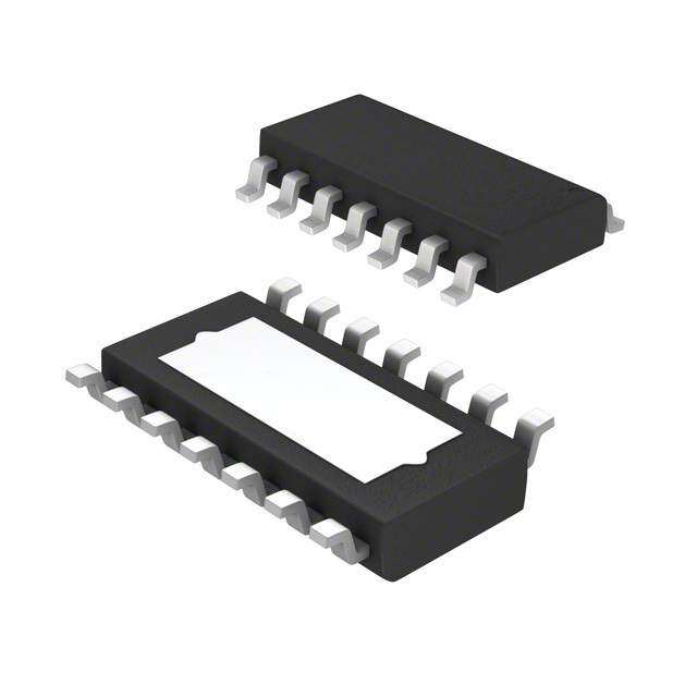
| 产品图片 |
|
| rohs | 符合RoHS无铅 / 符合限制有害物质指令(RoHS)规范要求 |
| 产品系列 | 开关 IC,USB开关IC,Diodes Incorporated AP2166SG-13- |
| 数据手册 | |
| 产品型号 | AP2166SG-13 |
| PCN设计/规格 | |
| Rds(On) | 135 毫欧 |
| RoHS指令信息 | http://diodes.com/download/4349 |
| 产品目录页面 | |
| 产品种类 | USB开关IC |
| 供应商器件封装 | 8-SOP |
| 其它名称 | AP2166SGDIDKR |
| 内部开关 | 是 |
| 包装 | Digi-Reel® |
| 商标 | Diodes Incorporated |
| 安装类型 | 表面贴装 |
| 安装风格 | SMD/SMT |
| 封装 | Reel |
| 封装/外壳 | 8-SOIC(0.154",3.90mm 宽) |
| 封装/箱体 | SOP-8 |
| 工作温度 | -40°C ~ 85°C |
| 工厂包装数量 | 2500 |
| 开关数量 | Dual |
| 最大工作温度 | + 85 C |
| 最小工作温度 | - 40 C |
| 标准包装 | 1 |
| 电压-输入 | 2.7 V ~ 5.5 V |
| 电流限制 | 1.5A |
| 类型 | USB 开关 |
| 系列 | AP2166 |
| 输出数 | 2 |


- 商务部:美国ITC正式对集成电路等产品启动337调查
- 曝三星4nm工艺存在良率问题 高通将骁龙8 Gen1或转产台积电
- 太阳诱电将投资9.5亿元在常州建新厂生产MLCC 预计2023年完工
- 英特尔发布欧洲新工厂建设计划 深化IDM 2.0 战略
- 台积电先进制程称霸业界 有大客户加持明年业绩稳了
- 达到5530亿美元!SIA预计今年全球半导体销售额将创下新高
- 英特尔拟将自动驾驶子公司Mobileye上市 估值或超500亿美元
- 三星加码芯片和SET,合并消费电子和移动部门,撤换高东真等 CEO
- 三星电子宣布重大人事变动 还合并消费电子和移动部门
- 海关总署:前11个月进口集成电路产品价值2.52万亿元 增长14.8%


PDF Datasheet 数据手册内容提取
AP2166/ AP2176 1A DUAL CHANNEL CURRENT-LIMITED POWER SWITCH Description Pin Assignments The AP2166 and AP2176 are integrated high-side power switches ( Top View ) optimized for Universal Serial Bus (USB) and other hot-swap applications. The family of devices complies with USB 2.0 and EN1 1 8 OUT1 available with both polarities of Enable input. They offer current and thermal limiting and short-circuit protection as well as controlled rise FLG1 2 7 IN time and under-voltage lockout functionality. A 7ms deglitch capability on the open-drain Flag output prevents false overcurrent reporting FLG2 3 6 GND and does not require any external components. EN2 4 5 OUT2 All devices are available in SO-8 and MSOP-8EP packages. SO-8 Features ( Top View ) Dual USB port power switches Overcurrent and thermal protection EN1 1 8 OUT1 1.5A accurate current limiting FLG1 2 7 IN Reverse Current Blocking 90mΩ on-resistance FLG2 3 6 GND Input voltage range: 2.7V - 5.5V EN2 4 5 OUT2 0.6ms typical rise time Very low shutdown current: 1µA (max) MSOP-8EP Fault report (FLG) with blanking time (7ms typ) ESD protection: 6KV HBM, 300V MM Applications Active low (AP2166) or active high (AP2176) enable Ambient temperature range -40°C to +85°C Consumer Electronics – LCD TVs & Monitors, Game Machines SO-8 and MSOP-8EP (Exposed Pad): Available in “Green” Communications – Set-Top-Boxes, GPS, Smartphones Molding Compound (No Br, Sb) Computing – Laptops, Desktops, Servers, Printers, Docking UL Recognized, File Number E322375 Stations, HUBs IEC60950-1 CB Scheme Certified Totally Lead-Free & Fully RoHS Compliant (Notes 1 & 2) Halogen and Antimony Free. “Green” Device (Note 3) Notes: 1. No purposely added lead. Fully EU Directive 2002/95/EC (RoHS) & 2011/65/EU (RoHS 2) compliant. 2. See http://www.diodes.com/quality/lead_free.html for more information about Diodes Incorporated’s definitions of Halogen- and Antimony-free, "Green" and Lead-free. 3. Halogen- and Antimony-free "Green” products are defined as those which contain <900ppm bromine, <900ppm chlorine (<1500ppm total Br + Cl) and <1000ppm antimony compounds. Typical Applications Circuit Power Supply IN OUT1 Load 2.7V to 5.5V 0.1uF 68uF 10k 10k 10uF 0.1uF FLG1 OUT2 Load FLG2 0.1uF 68uF ON EN1 OFF EN2 GND AP2166/ AP2176 1 of 17 May 2016 Document number: DS31814 Rev. 4 - 2 www.diodes.com © Diodes Incorporated
AP2166/ AP2176 Available Options Enable Pin Current Limit Recommended Maximum Part Number Channel (EN) (typ) Continuous Load Current AP2166 2 Active Low 1.5A 1.0A AP2176 2 Active High 1.5A 1.0A Pin Descriptions Pin Number Pin Name Function SO-8 MSOP-8EP EN1 1 1 Switch 1 enable input, active low (AP2166) or active high (AP2176) FLG1 2 2 Switch 1 over-current and over-temperature fault report, open-drain FLG2 3 3 Switch 2 over-current and over-temperature fault report, open-drain EN2 4 4 Switch 2 enable input, active low (AP2166) or active high (AP2176) OUT2 5 5 Switch 2 voltage output pin GND 6 6 Ground IN 7 7 Voltage input pin OUT1 8 8 Switch 1 voltage output pin Exposed Pad: Exposed Pad — Exposed Pad It should be connected externally to GND and thermal mass for enhanced thermal impedance. It should not be used as electrical ground conduction path. Functional Block Diagram FLG1 Thermal Sense Deglitch EN1 Driver Current Limit UVLO GND CS OUT1 Reverse blocking IN Reverse blocking CS OUT2 UVLO FLG2 Current Driver EN2 Limit Deglitch Thermal Sense GND AP2166/ AP2176 2 of 17 May 2016 Document number: DS31814 Rev. 4 - 2 www.diodes.com © Diodes Incorporated
AP2166/ AP2176 Absolute Maximum Ratings (@TA = +25°C, unless otherwise specified.) Symbol Parameter Rating Unit ESD HBM Human Body Model ESD Protection 6 kV ESD MM Machine Model ESD Protection 300 V VIN Input Voltage 6.5 V VOUT Output Voltage VIN +0.3 V VEN , VFLG Enable Voltage 6.5 V ILOAD Maximum Continuous Load Current Internal Limited A TJ(MAX) Maximum Junction Temperature +150 °C TST Storage Temperature Range (Note 4) -65 to +150 °C Note: 4. UL Recognized Rating from -30°C to +70°C (Diodes qualified TST from -65°C to +150°C). Recommended Operating Conditions (@TA = +25°C, unless otherwise specified.) Symbol Parameter Min Max Units VIN Input Voltage 2.7 5.5 V IOUT Output Current 0 1.0 A VIL Low-Level Input Voltage on EN or EN 0 0.8 V VIH High-Level Input Voltage on EN or EN 2 VIN V TA Operating Ambient Temperature -40 +85 C AP2166/ AP2176 3 of 17 May 2016 Document number: DS31814 Rev. 4 - 2 www.diodes.com © Diodes Incorporated
AP2166/ AP2176 Electrical Characteristics (@TA = +25°C, CIN = 10µF, VIN = +5V, unless otherwise specified.) Symbol Parameter Test Conditions Min Typ Max Unit VUVLO Input UVLO RLOAD = 1kΩ 1.6 1.9 2.5 V ISHDN Input Shutdown Current Disabled, IOUT = 0 - 0.5 1 µA IQ Input Quiescent Current, Dual Enabled, IOUT = 0 - 95 140 µA ILEAK Input Leakage Current Disabled, OUT grounded - - 1 µA IREV Reverse Leakage Current Disabled, VIN = 0V, VOUT = 5V, IREV at VIN - 1 - µA MSOP-8EP - 90 135 mΩ VIN = 5V, IOUT = 1A, -40°C ≤ TA ≤ +85°C RDS(ON) Switch On-Resistance SO-8 - 100 135 mΩ VIN = 3.3V, IOUT = 1A, -40°C ≤ TA ≤ +85°C - 120 160 mΩ ISHORT Short-Circuit Current Limit Enabled into short circuit, CL = 68µF - 1.5 - A ILIMIT Overload Current Limit VIN = 5V, VOUT = 4.8V, CL = 120µF, -40°C ≤ TA ≤ +85°C 1.1 1.5 1.9 A ITrig Current Limiting Trigger Threshold VIN = VEN, Output Current Slew rate (<100A/WS), CL = 68µF - 2.0 - A TSHORT Short-Circuit Response Time VOUT = 0V to IOUT = ILIMIT (short applied to output), CL = 68µF - 20 - µs VIL EN Input Logic Low Voltage VIN = 2.7V to 5.5V - - 0.8 V VIH EN Input Logic High Voltage VIN = 2.7V to 5.5V 2 - - V ISINK EN Input Leakage VEN = 5V - - 1 µA TD(ON) Output Turn-on Delay Time CL=1µF, RLOAD = 10Ω - 0.05 - ms TR Output Turn-on Rise Time CL=1µF, RLOAD = 10Ω - 0.6 1.5 ms TD(OFF) Output Turn-off Delay Time CL=1µF, RLOAD = 10Ω - 0.01 - ms TF Output Turn-off Fall Time CL=1µF, RLOAD = 10Ω - 0.05 0.1 ms RFLG FLG Output FET on-Resistance IFLG =10mA - 20 40 Ω IFOH Error Flag Iff Current VFLG = 5V - 0.01 1 µA TBlank FLG Blanking Time CL = 68µF 4 7 15 ms TSHDN Thermal Shutdown Threshold Enabled, RLOAD = 1kΩ - +140 - C THYS Thermal Shutdown Hysteresis - - +25 - C SO-8 (Note 5) - 110 - °C/W θJA Thermal Resistance Junction-to-Ambient MSOP-8EP (Note 6) - 60 - °C/W Notes: 5. Test condition for SO-8: Device mounted on FR-4 2-layer board, 2oz. copper, with minimum recommended pad layout. 6. Test condition for MSOP-8EP: Device mounted on FR-4 2-layer board, 2oz. copper, with minimum recommended pad on top layer and 3 vias to bottom layer ground plane. AP2166/ AP2176 4 of 17 May 2016 Document number: DS31814 Rev. 4 - 2 www.diodes.com © Diodes Incorporated
AP2166/ AP2176 Typical Performance Characteristics V V EN 50% 50% EN 50% 50% T T T D(OFF) T D(OFF) R R T T F F T T D(ON) 90% 90% D(ON) 90% 90% V V OUT OUT 10% 10% 10% 10% Figure 1 Voltage Waveforms: AP2166 (left), AP2176 (right) All Enable Plots are for AP2176 Active High Ven 1 Ven 1 5V/div 5V/div CL=1µF Vout 1 Vout 1 TA= +25°C 2V/div 2V/div RL=10Ω CL=1µF TA= +25°C RL=10Ω 500µs/div 500µs/div Channel 1 Turn-On Delay and Rise Time Channel 1 Turn-Off Delay and Fall Time AP2166/ AP2176 5 of 17 May 2016 Document number: DS31814 Rev. 4 - 2 www.diodes.com © Diodes Incorporated
AP2166/ AP2176 Typical Performance Characteristics (continued) Ven 2 Ven 2 5V/div 5V/div CL=1µF Vout 2 Vout 2 TA= +25°C 2V/div 2V/div RL=10Ω CL=1µF TA= +25°C RL=10Ω 500µs/div 500µs/div Channel 2 Turn-On Delay and Rise Time Channel 2 Turn-Off Delay and Fall Time Ven 1 Ven 1 5V/div 5V/div CL=100µF TA= +25°C Vout 1 Vout 1 2V/div 2V/div RL=10Ω CL=100µF TA= +25°C RL=10Ω 500µs/div 500µs/div Channel 1 Turn-On Delay and Rise Time Channel 1 Turn-Off Delay and Fall Time Ven 2 Ven 2 5V/div 5V/div CL=100µF TA= +25°C Vout 2 Vout 2 RL=10Ω 2V/div 2V/div CL=100µF TA= +25°C RL=10Ω 500µs/div 500µs/div Channel 2 Turn-On Delay and Rise Time Channel 2 Turn-Off Delay and Fall Time AP2166/ AP2176 6 of 17 May 2016 Document number: DS31814 Rev. 4 - 2 www.diodes.com © Diodes Incorporated
AP2166/ AP2176 Typical Performance Characteristics (cont.) Ven 1 Ven 2 5V/div 5V/div Iout 1 Iout 2 500mA/div 500mA/div VIN=5V VIN=5V TA= +25°C TA= +25°C CL=68µF CL=68µF 500µs/div 500µs/div Channel 1 Short Circuit Current, Channel 2 Short Circuit Current, Device Enabled Into Short Device Enabled Into Short Ven 1 5V/div CL=100µF V5Ven/d 2iv CL=100µF VIN=5V VIN=5V TA= +25°C TA= +25°C RL=5Ω RL=5Ω Iout 1 Iout 2 200mA/div 200mA/div CL=470µF CL=470µF CL=220µF CL=220µF 1ms/div 1ms/div Channel 1 Inrush Current Channel 2 Inrush Current VIN=5V VIN=5V TA= +25°C TA= +25°C Vflag 1 Vflag 1 2V/div CL=68µF 2V/div CL=68µF Iout 1 Iout 1 1A/div 1A/div 2ms/div 2ms/div Channel 1 Channel 1 1Ω Load Connected to Enabled Device 2Ω Load Connected to Enabled Device AP2166/ AP2176 7 of 17 May 2016 Document number: DS31814 Rev. 4 - 2 www.diodes.com © Diodes Incorporated
AP2166/ AP2176 Typical Performance Characteristics (cont.) VIN=5V VIN=5V TA= +25°C TA= +25°C Vflag 2 Vflag 2 2V/div CL=68µF 2V/div CL=68µF Iout 2 Iout 2 1A/div 1A/div 2ms/div 2ms/div Channel 2 Channel 2 1Ω Load Connected to Enabled Device 2Ω Load Connected to Enabled Device V5Vou/dti v VIN=5V V5Vou/dti v VIN=5V TCAL== 6+82µ5F° C TCAL== 6+82µ5F° C Vflag Iout 5V/div 500mA/div Iout Iout 1A/div 1A/div 20ms/div 20ms/div Channel 1 Channel 2 Short Circuit with Blanking Time and Recovery Short Circuit with Blanking Time and Recovery Vflag Vflag 5V/div 5V/div Iout Iout 500mA/div TA= +25°C 500mA/div TA= +25°C CL=68µF CL=68µF RL=5Ω RL=5Ω Ven Ven 5V/div 5V/div Vin Vin 5V/div 5V/div 1ms/div 1ms/div Channel 2 Power On Channel 1 Power On AP2166/ AP2176 8 of 17 May 2016 Document number: DS31814 Rev. 4 - 2 www.diodes.com © Diodes Incorporated
AP2166/ AP2176 Typical Performance Characteristics (cont.) TA= +25°C CL=68µF Vin Vin 2V/div 2V/div RL=5Ω TA= +25°C CL=68µF RL=5Ω Iout Iout 500mA/div 500mA/div 1ms/div 10ms/div Channel 1 UVLO Increasing Channel 1 UVLO Decreasing TA= +25°C CL=68µF Vin Vin 2V/div 2V/div RL=5Ω TA= +25°C CL=68µF RL=5Ω Iout Iout 500mA/div 500mA/div 1ms/div 10ms/div Channel 2 UVLO Increasing Channel 2 UVLO Decreasing Vout 1 5V/div Ven1 5V/div Vout 2 Vout 1 5V/div 5V/div Vflag 1 Ven2 5V/div TA= +25°C 5V/div TA= +25°C CL=68µF CL=68µF Iout 2 Vout 2 500mA/div 5V/div 100ms/div 50ms/div Channel 1 Enabled and Shorted with Channel 2 Channel 1 Disabled and Channel 2 Enabled Disabled AP2166/ AP2176 9 of 17 May 2016 Document number: DS31814 Rev. 4 - 2 www.diodes.com © Diodes Incorporated
AP2166/ AP2176 Typical Performance Characteristics (cont.) Turn-On Time vs Input Voltage Turn-Off Time vs Input Voltage 750 30 700 29 CL=1µF 650 29 RL=10Ω us) 600 us) 28 TA= +25°C e ( 550 e ( m m 28 n-On Ti 455000 n-Off Ti 27 Tur 400 CL=1µF Tur 27 350 RL=10Ω 26 300 TA= +25°C 26 250 25 1.5 2 2.5 3 3.5 4 4.5 5 5.5 6 1.5 2 2.5 3 3.5 4 4.5 5 5.5 6 Input Voltage (V) Input Voltage (V) Rise Time vs Input Voltage Fall Time vs Input Voltage 650 22 600 22 550 Rise Time (us) 445050000 CL=1µF Fall Time (us) 222011 CL=1µF 350 RL=10Ω RL=10Ω 300 TA= +25°C 20 TA= +25°C 250 19 2 2.5 3 3.5 4 4.5 5 5.5 6 2 2.5 3 3.5 4 4.5 5 5.5 6 Input Voltage (V) Input Voltage (V) Supply Current, Output Enabled vs Ambient Temperature Supply Current, Output Disabled vs Ambient Temperature 68 A) A) Vin=5.5V urrent, Output Enabled (u 4455638383 Vin=5.5V Vin=5.0V urrent, Output Disabled (u 000000......345678 V in=3.3V V in=5.0V upply C 3338 Vin=3.3V Vin=2.7V upply C 00..12 S S Vin=2.7V 28 0.0 -60 -40 -20 0 20 40 60 80 100 -60 -40 -20 0 20 40 60 80 100 Ambient Temperature (°C) Ambient Temperature (°C) AP2166/ AP2176 10 of 17 May 2016 Document number: DS31814 Rev. 4 - 2 www.diodes.com © Diodes Incorporated
AP2166/ AP2176 Typical Performance Characteristics (cont.) Static Drain-Source On-State Resistance vs Ambient Short-Circuit Output Current vs Ambient Temperature Temperature 1.56 170 1.55 Vin=2.7V A) CL=100µF Vin=3.3V Drain-Source On-State Resistance (mΩ) 111111123456000000 V in=3.3V Circuit Output Current ( 1111111.......44555558901234 V in=2.7V V in=5.0V Static 10900 V in=5V Short- 11..4467 Vin=5.5V 80 1.45 -60 -40 -20 0 20 40 60 80 100 -60 -40 -20 0 20 40 60 80 100 Ambient Temperature (°C) Ambient Temperature (°C) Undervoltage Lockout vs Ambient Temperature Threshold Trip Current vs Input Voltage 2.20 1.99 1.98 ckout (V) 22..0100 UVLO Rising urrent (A) 111...999567 Undervoltage Lo 111...789000 UVLO Falling Threshold Trip C 11111.....9999901234 TCAL== 6+82µ5F° C 1.89 1.60 1.88 -60 -40 -20 0 20 40 60 80 100 2.8 3.3 3.8 4.3 4.8 5.3 Ambient Temperature (°C) Input Voltage (V) Current Limit Response vs Peak Current 120 s) 100 u e ( ns 80 o sp VIN=5V e mit R 60 TA= +25° C Li CL=68µF nt 40 e urr C 20 0 0 2 4 6 8 10 12 Peak Current (A) AP2166/ AP2176 11 of 17 May 2016 Document number: DS31814 Rev. 4 - 2 www.diodes.com © Diodes Incorporated
AP2166/ AP2176 Application Information Power Supply Considerations A 0.01-μF to 0.1-μF X7R or X5R ceramic bypass capacitor between IN and GND, close to the device, is recommended. Placing a high-value electrolytic capacitor on the input (10-μF minimum) and output pin(s) is recommended when the output load is heavy. This precaution reduces power-supply transients that may cause ringing on the input. Additionally, bypassing the output with a 0.01-μF to 0.1-μF ceramic capacitor improves the immunity of the device to short-circuit transients. Overcurrent and Short Circuit Protection An internal sensing FET is employed to check for over-current conditions. Unlike current-sense resistors, sense FETs do not increase the series resistance of the current path. When an overcurrent condition is detected, the device maintains a constant output current and reduces the output voltage accordingly. Complete shutdown occurs only if the fault stays long enough to activate thermal limiting. Three possible overload conditions can occur. In the first condition, the output has been shorted to GND before the device is enabled or before VIN has been applied. The AP2166/AP2176 senses the short circuit and immediately clamps output current to a certain safe level namely ILIMIT. In the second condition, an output short or an overload occurs while the device is enabled. At the instance the overload occurs, higher current may flow for a very short period of time before the current limit function can react. After the current limit function has tripped (reached the overcurrent trip threshold), the device switches into current limiting mode and the current is clamped at ILIMIT. In the third condition, the load has been gradually increased beyond the recommended operating current. The current is permitted to rise until the current-limit threshold (ITRIG) is reached or until the thermal limit of the device is exceeded. The AP2166/AP2176 is capable of delivering current up to the current-limit threshold without damaging the device. Once the threshold has been reached, the device switches into its current limiting mode and is set at ILIMIT. Note that when the output has been shorted to GND at extremely low temperature (< -30°C), a minimum 120-μF electrolytic capacitor on the output pin is recommended. A correct capacitor type with capacitor voltage rating and temperature characteristics must be properly chosen so that capacitance value does not drop too low at the extremely low temperature operation. A recommended capacitor should have temperature characteristics of less than 10% variation of capacitance change when operated at extremely low temp. Our recommended aluminum electrolytic capacitor type is Panasonic FC series. FLG Response When an overcurrent or over-temperature shutdown condition is encountered, the FLG open-drain output goes active low after a nominal 7-ms deglitch timeout. The FLG output remains low until both overcurrent and over-temperature conditions are removed. Connecting a heavy capacitive load to the output of the device can cause a momentary overcurrent condition, which does not trigger the FLG due to the 7-ms deglitch timeout. The AP2166/AP2176 is designed to eliminate false overcurrent reporting without the need of external components to remove unwanted pulses. Power Dissipation and Junction Temperature The low on-resistance of the internal MOSFET allows the small surface-mount packages to pass large current. Using the maximum operating ambient temperature (TA) and RDS(ON), the power dissipation can be calculated by: PD = RDS(ON)× I2 Finally, calculate the junction temperature: TJ = PD x RθJA + TA Where: TA= Ambient temperature C RθJA = Thermal resistance PD = Total power dissipation Thermal Protection Thermal protection prevents the IC from damage when heavy-overload or short-circuit faults are present for extended periods of time. The AP2166/AP2176 implements a thermal sensing to monitor the operating junction temperature of the power distribution switch. Once the die temperature rises to approximately +140°C due to excessive power dissipation in an overcurrent or short-circuit condition the internal thermal sense circuitry turns the power switch off, thus preventing the power switch from damage. Hysteresis is built into the thermal sense circuit allowing the device to cool down approximately +25°C before the switch turns back on. The switch continues to cycle in this manner until the load fault or input power is removed. The FLG open-drain output is asserted when an over-temperature shutdown or overcurrent occurs with 7-ms deglitch. AP2166/ AP2176 12 of 17 May 2016 Document number: DS31814 Rev. 4 - 2 www.diodes.com © Diodes Incorporated
AP2166/ AP2176 Application Information (continued) Undervoltage Lockout (UVLO) Undervoltage lockout function (UVLO) keeps the internal power switch from being turned on until the power supply has reached at least 1.9V, even if the switch is enabled. Whenever the input voltage falls below approximately 1.9V, the power switch is quickly turned off. This facilitates the design of hot-insertion systems where it is not possible to turn off the power switch before input power is removed. Host/Self-Powered HUBs Hosts and self-powered hubs (SPH) have a local power supply that powers the embedded functions and the downstream ports (see Figure 2). This power supply must provide from 5.25V to 4.75V to the board side of the downstream connection under both full-load and no-load conditions. Hosts and SPHs are required to have current-limit protection and must report overcurrent conditions to the USB controller. Typical SPHs are desktop PCs, monitors, printers, and stand-alone hubs. Power Supply Downstream USB Ports 3.3V 5V D+ AP2166 D- IN OUT1 VBUS 0.1uF 0.1uF 68uF GND FLG1 D+ USB EN1 D- Controller FLG2 EN2 OUT2 VBUS GND 0.1uF 68uF GND Figure 2 Typical Two-Port USB Host/ Self-Powered Hub Generic Hot-Plug Applications In many applications it may be necessary to remove modules or PC boards while the main unit is still operating. These are considered hot-plug applications. Such implementations require the control of current surges seen by the main power supply and the card being inserted. The most effective way to control these surges is to limit and slowly ramp the current and voltage being applied to the card, similar to the way in which a power supply normally turns on. Due to the controlled rise times and fall times of the AP2166/AP2176, these devices can be used to provide a softer start-up to devices being hot-plugged into a powered system. The UVLO feature of the AP2166/AP2176 also ensures that the switch is off after the card has been removed, and that the switch is off during the next insertion. By placing the AP2166/AP2176 between the VCC input and the rest of the circuitry, the input power reaches these devices first after insertion. The typical rise time of the switch is approximately 1ms, providing a slow voltage ramp at the output of the device. This implementation controls system surge current and provides a hot-plugging mechanism for any device. AP2166/ AP2176 13 of 17 May 2016 Document number: DS31814 Rev. 4 - 2 www.diodes.com © Diodes Incorporated
AP2166/ AP2176 Ordering Information AP 21 X 6 XX G - 13 Enable Channel Package Green Packing 6 : Active Low 6 : 2 Channel S : SO-8 G : Green 13 : Tape & Reel 7 : Active High MP : MSOP-8EP 13” Tape and Reel Part Number Package Code Packaging Quantity Part Number Suffix AP21X6SG-13 S SO-8 2,500/Tape & Reel -13 AP21X6MPG-13 MP MSOP-8EP 2,500/Tape & Reel -13 Marking Information (1) SO-8 ( Top view ) 8 7 6 5 Logo 6 : 2 Channel Part Number AP21X X G : Green 6 : Active Low YY : Year : 08, 09,10~ YY WW X X 7 : Active High WW : Week : 01~52; 52 represents 52 and 53 week X : Internal Code 1 2 3 4 (2) MSOP-8EP AP2166/ AP2176 14 of 17 May 2016 Document number: DS31814 Rev. 4 - 2 www.diodes.com © Diodes Incorporated
AP2166/ AP2176 Package Outline Dimensions (All dimensions in mm.) Please see http://www.diodes.com/package-outlines.html for the latest version. (1) Package type: SO-8 SO-8 54 Dim Min Max E1 E 0.2 Gauge Plane A - 1.75 A1 Seating Plane A1 0.10 0.20 L A2 1.30 1.50 Detail ‘A’ A3 0.15 0.25 b 0.3 0.5 D 4.85 4.95 h 7°~9° E 5.90 6.10 45° E1 3.85 3.95 Detail ‘A’ A2 A A3 e 1.27 Typ h - 0.35 e b L 0.62 0.82 D 0 8 All Dimensions in mm (2) Package type: MSOP-8EP D MSOP-8EP Dim Min Max Typ A - 1.10 - A1 0.05 0.15 0.10 D1 4X10° AA23 00..7259 00..9459 00..8369 x 5 E E2 0.2 b 0.22 0.38 0.30 Gauge Plane c 0.08 0.23 0.15 y Seating Plane D 2.90 3.10 3.00 a D1 1.60 2.00 1.80 1 e 8Xb 4X10° L EE1 42..7900 53..1100 43..9000 E3 Detail C E2 1.30 1.70 1.50 A1 A3 E3 2.85 3.05 2.95 c e - - 0.65 A A2 L 0.40 0.80 0.60 D E1 a 0° 8° 4° x - - 0.750 See Detail C y - - 0.750 All Dimensions in mm AP2166/ AP2176 15 of 17 May 2016 Document number: DS31814 Rev. 4 - 2 www.diodes.com © Diodes Incorporated
AP2166/ AP2176 Suggested Pad Layout Please see http://www.diodes.com/package-outlines.html for the latest version. (1) Package type: SO-8 X Dimensions Value (in mm) X 0.60 Y 1.55 C1 C1 5.4 C2 1.27 C2 Y (2) Package type: MSOP-8EP X C G Y Dimensions Value (in mm) C 0.650 G 0.450 X 0.450 Y2 Y1 X1 2.000 X1 Y 1.350 Y1 1.700 Y2 5.300 AP2166/ AP2176 16 of 17 May 2016 Document number: DS31814 Rev. 4 - 2 www.diodes.com © Diodes Incorporated
AP2166/ AP2176 IMPORTANT NOTICE DIODES INCORPORATED MAKES NO WARRANTY OF ANY KIND, EXPRESS OR IMPLIED, WITH REGARDS TO THIS DOCUMENT, INCLUDING, BUT NOT LIMITED TO, THE IMPLIED WARRANTIES OF MERCHANTABILITY AND FITNESS FOR A PARTICULAR PURPOSE (AND THEIR EQUIVALENTS UNDER THE LAWS OF ANY JURISDICTION). Diodes Incorporated and its subsidiaries reserve the right to make modifications, enhancements, improvements, corrections or other changes without further notice to this document and any product described herein. Diodes Incorporated does not assume any liability arising out of the application or use of this document or any product described herein; neither does Diodes Incorporated convey any license under its patent or trademark rights, nor the rights of others. Any Customer or user of this document or products described herein in such applications shall assume all risks of such use and will agree to hold Diodes Incorporated and all the companies whose products are represented on Diodes Incorporated website, harmless against all damages. Diodes Incorporated does not warrant or accept any liability whatsoever in respect of any products purchased through unauthorized sales channel. Should Customers purchase or use Diodes Incorporated products for any unintended or unauthorized application, Customers shall indemnify and hold Diodes Incorporated and its representatives harmless against all claims, damages, expenses, and attorney fees arising out of, directly or indirectly, any claim of personal injury or death associated with such unintended or unauthorized application. Products described herein may be covered by one or more United States, international or foreign patents pending. Product names and markings noted herein may also be covered by one or more United States, international or foreign trademarks. This document is written in English but may be translated into multiple languages for reference. Only the English version of this document is the final and determinative format released by Diodes Incorporated. LIFE SUPPORT Diodes Incorporated products are specifically not authorized for use as critical components in life support devices or systems without the express written approval of the Chief Executive Officer of Diodes Incorporated. As used herein: A. Life support devices or systems are devices or systems which: 1. are intended to implant into the body, or 2. support or sustain life and whose failure to perform when properly used in accordance with instructions for use provided in the labeling can be reasonably expected to result in significant injury to the user. B. A critical component is any component in a life support device or system whose failure to perform can be reasonably expected to cause the failure of the life support device or to affect its safety or effectiveness. Customers represent that they have all necessary expertise in the safety and regulatory ramifications of their life support devices or systems, and acknowledge and agree that they are solely responsible for all legal, regulatory and safety-related requirements concerning their products and any use of Diodes Incorporated products in such safety-critical, life support devices or systems, notwithstanding any devices- or systems-related information or support that may be provided by Diodes Incorporated. Further, Customers must fully indemnify Diodes Incorporated and its representatives against any damages arising out of the use of Diodes Incorporated products in such safety-critical, life support devices or systems. Copyright © 2016, Diodes Incorporated www.diodes.com AP2166/ AP2176 17 of 17 May 2016 Document number: DS31814 Rev. 4 - 2 www.diodes.com © Diodes Incorporated