ICGOO在线商城 > 集成电路(IC) > PMIC - 稳压器 - 线性 > AP2114H-3.3TRG1
 Datasheet下载
- 型号: AP2114H-3.3TRG1
- 制造商: Diodes Inc.
- 库位|库存: xxxx|xxxx
- 要求:
| 数量阶梯 | 香港交货 | 国内含税 |
| +xxxx | $xxxx | ¥xxxx |
查看当月历史价格
查看今年历史价格
AP2114H-3.3TRG1产品简介:
ICGOO电子元器件商城为您提供AP2114H-3.3TRG1由Diodes Inc.设计生产,在icgoo商城现货销售,并且可以通过原厂、代理商等渠道进行代购。 AP2114H-3.3TRG1价格参考。Diodes Inc.AP2114H-3.3TRG1封装/规格:PMIC - 稳压器 - 线性, Linear Voltage Regulator IC Positive Fixed 1 Output 1A SOT-223。您可以下载AP2114H-3.3TRG1参考资料、Datasheet数据手册功能说明书,资料中有AP2114H-3.3TRG1 详细功能的应用电路图电压和使用方法及教程。
| 参数 | 数值 |
| 产品目录 | 集成电路 (IC) |
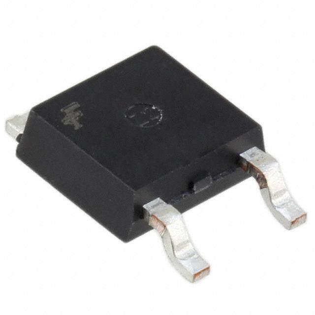
| 描述 | IC REG LDO 3.3V 1A SOT223 |
| 产品分类 | |
| 品牌 | Diodes Incorporated |
| 数据手册 | |
| 产品图片 |
|
| 产品型号 | AP2114H-3.3TRG1 |
| rohs | 无铅 / 符合限制有害物质指令(RoHS)规范要求 |
| RoHS指令信息 | http://diodes.com/download/4349 |
| 产品系列 | - |
| 供应商器件封装 | SOT-223 |
| 其它名称 | AP2114H-3.3TRG1DICT |
| 包装 | 剪切带 (CT) |
| 安装类型 | 表面贴装 |
| 封装/外壳 | TO-261-4,TO-261AA |
| 工作温度 | -40°C ~ 85°C |
| 标准包装 | 1 |
| 电压-跌落(典型值) | 0.45V @ 1A |
| 电压-输入 | 最高 6V |
| 电压-输出 | 3.3V |
| 电流-输出 | 1A |
| 电流-限制(最小值) | - |
| 稳压器拓扑 | 正,固定式 |
| 稳压器数 | 1 |


- 商务部:美国ITC正式对集成电路等产品启动337调查
- 曝三星4nm工艺存在良率问题 高通将骁龙8 Gen1或转产台积电
- 太阳诱电将投资9.5亿元在常州建新厂生产MLCC 预计2023年完工
- 英特尔发布欧洲新工厂建设计划 深化IDM 2.0 战略
- 台积电先进制程称霸业界 有大客户加持明年业绩稳了
- 达到5530亿美元!SIA预计今年全球半导体销售额将创下新高
- 英特尔拟将自动驾驶子公司Mobileye上市 估值或超500亿美元
- 三星加码芯片和SET,合并消费电子和移动部门,撤换高东真等 CEO
- 三星电子宣布重大人事变动 还合并消费电子和移动部门
- 海关总署:前11个月进口集成电路产品价值2.52万亿元 增长14.8%


PDF Datasheet 数据手册内容提取
Data Sheet 1A LOW NOISE CMOS LDO REGUL ATOR WITH ENABLE AP2114 General Description Features The AP2114 is CMOS process low dropout linear • Output Voltage Accuracy: ±1.5% regulator with enable function, the regulator delivers • Output Current: 1A (Min) a guaranteed 1A (Min) continuous load current. • Fold-back Short Current Protection: 50mA • Low Dropout Voltage (3.3V): 450mV (Typ) The AP2114 features low power consumption. @I =1A OUT • Stable with 4.7μF Flexible Cap: Ceramic, The AP2114 is available in 1.2V, 1.5V, 1.8V, 2.5V Tantalum and Aluminum Electrolytic and 3.3V regulator output and 0.8V to 5V adjustable • Excellent Line Regulation: 0.02%/V (Typ), output, and available in excellent output accuracy 0.1%/V (Max) @ IOUT=30mA ±1.5%, it is also available in an excellent load • Excellent Load Regulation: 0.2%A (Typ) @ regulation and line regulation performance. IOUT=1mA to 1A • Low Quiescent Current: 60μA (1.2V/1.5V/1.8V The AP2114 is available in standard packages of /2.5V/ADJ) SOT-223, TO-252-2 (1), TO-252-2 (3), TO-252-2 (4), • Low Output Noise: 30μVRMS TO-263-3, SOIC-8 and PSOP-8. • PSRR: 68dB @ Freq=1KHz (1.2V/1.5V/1.8V /ADJ) • OTSD Protection • Operating Temperature Range: -40°C to 85°C • ESD: MM 400V, HBM 4000V Applications • LCD Monitor • LCD TV • STB SOT-223 TO-263-3 TO-252-2 (1) TO-252-2 (3) TO-252-2 (4) SOIC-8 PSOP-8 Figure 1. Package Types of AP2114 Jan. 2013 Rev. 2. 2 BCD Semiconductor Manufacturing Limited 1
Data Sheet 1A LOW NOISE CMOS LDO REGULATOR WITH ENABLE AP2114 Pin Configuration H/HA Package S Package (SOT-223) (TO-263-3) H HA D/DA Package D DA (TO-252-2 (1)) (TO-252-2 (3)) (TO-252-2 (1)) (TO-252-2 (3)) 3 VIN 3 VIN 3 VOUT 3 VOUT V OUT 2 VOUTVOUT 2 VOUT GND 2 GND GND 2 GND 1 GND 1 GND 1 VIN 1 VIN (TO-252-2 (4)) (TO-252-2 (4)) 3 VIN 3 VOUT VOUT 2 VOUT GND 2 GND 1 GND 1 VIN M Package MP Package (SOIC-8) (PSOP-8) GND 1 8 EN VIN 1 8 VOUT GND 1 8 EN VIN 1 8 VOUT VOUT 2 7 GNDGND 2 7 GND VOUT 2 7 GND GND 2 7 GND GND 3 6 GNDGN D 3 6 ADJ GND 3 6 GND GND 3 6 ADJ VIN 4 5 GND EN 4 5 GND VIN 4 5 GND EN 4 5 GND For Fixed Versions For Adjustable Version For Fixed Versions For Adjustable Version Figure 2. Pin Configuration of AP2114 (Top View) Jan. 2013 Rev. 2. 2 BCD Semiconductor Manufacturing Limited 2
Data Sheet 1A LOW NOISE CMOS LDO REGULATOR WITH ENABLE AP2114 Pin Descriptions Pin Number SOT-223 (H), SOT-223 (HA), Pin Function TO-263-3, SOIC-8, SOIC-8, TO-252-2 (1) (DA) TO-252-2 (1) (D) PSOP-8 PSOP-8 Name TO-252-2 (3) (DA) TO-252-2 (3) (D) (Fixed) (ADJ) TO-252-2 (4) (DA) TO-252-2 (4) (D) 1 2 1, 3, 5, 6, 7 2, 3, 5, 7 GND Ground 2 3 2 8 VOUT Regulated Output 3 1 4 1 VIN Input Voltage Pin Chip Enable, H–Normal 8 4 EN Work, L– Shutdown Output 6 ADJ Adjust Output Functional Block Diagram (8) 3 (4){1} EN Shutdown VIN Logic Thermal Foldback Shutdown Current Limit 2 (2){3} VOUT 3MΩ VREF GND 1 (1, 3, 5, 6, 7){2} A (B){C} A: SOT-223(H), TO-263-3, TO-252-2 (1)/(3)/(4)(D) B: SOIC-8, PSOP-8 C: SOT-223(HA), TO -252-2 (1)/(3)/(4)(DA) For Fixed Versions Jan. 2013 Rev. 2. 2 BCD Semiconductor Manufacturing Limited 3
Data Sheet 1A LOW NOISE CMOS LDO REGULATOR WITH ENABLE AP2114 Functional Block Diagram (Continued) 4 1 EN Shutdown VIN Logic Thermal Foldback Shutdown Current Limit 3MΩ 8 VOUT VREF 6 2, 3, 5, 7 ADJ GND SOIC-8, PSOP-8 For ADJ Version Figure 3. Functional Block Diagram of AP2114 Jan. 2013 Rev. 2. 2 BCD Semiconductor Manufacturing Limited 4
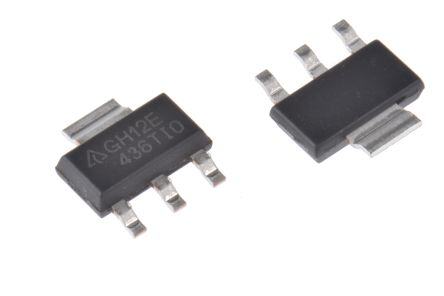
Data Sheet 1A LOW NOISE CMOS LDO REGULATOR WITH ENABLE AP2114 Ordering Information AP2114 - Circuit Type G1: Green Package Blank: Tube H/HA: SOT-223 TR: Tape & Reel D/DA: TO-252-2 (1)/(3)/(4) 1.2: Fixed Output 1.2V S: TO-263-3 1.5: Fixed Output 1.5V M: SOIC-8 1.8: Fixed Output 1.8V MP: PSOP-8 2.5: Fixed Output 2.5V 3.3: Fixed Output 3.3V ADJ: ADJ Output Temperature Output Packing Package Part Number Marking ID Range Voltage Type 1.2V (H) AP2114H-1.2TRG1 GH12C Tape & Reel 1.5V (H) AP2114H-1.5TRG1 GH16G Tape & Reel SOT-223 -40 to 85°C 1.8V (H) AP2114H-1.8TRG1 GH12D Tape & Reel 2.5V (H) AP2114H-2.5TRG1 GH14C Tape & Reel 3.3V (H) AP2114H-3.3TRG1 GH12E Tape & Reel 1.2V (HA) AP2114HA-1.2TRG1 GH13B Tape & Reel 1.5V (HA) AP2114HA-1.5TRG1 GH16H Tape & Reel SOT-223 -40 to 85°C 1.8V (HA) AP2114HA-1.8TRG1 GH14D Tape & Reel 2.5V (HA) AP2114HA-2.5TRG1 GH14E Tape & Reel 3.3V (HA) AP2114HA-3.3TRG1 GH14F Tape & Reel 1.2V (D) AP2114D-1.2TRG1 AP2114D-1.2G1 Tape & Reel TO-252-2 (1)/ 1.5V (D) AP2114D-1.5TRG1 AP2114D-1.5G1 Tape & Reel TO-252-2 (3)/ -40 to 85°C 1.8V (D) AP2114D-1.8TRG1 AP2114D-1.8G1 Tape & Reel TO-252-2 (4) 2.5V (D) AP2114D-2.5TRG1 AP2114D-2.5G1 Tape & Reel 3.3V (D) AP2114D-3.3TRG1 AP2114D-3.3G1 Tape & Reel 1.2V (DA) AP2114DA-1.2TRG1 AP2114DA-1.2G1 Tape & Reel TO-252-2 (1)/ 1.5V (DA) AP2114DA-1.5TRG1 AP2114DA-1.5G1 Tape & Reel TO-252-2 (3)/ -40 to 85°C 1.8V (DA) AP2114DA-1.8TRG1 AP2114DA-1.8G1 Tape & Reel TO-252-2 (4) 2.5V (DA) AP2114DA-2.5TRG1 AP2114DA-2.5G1 Tape & Reel 3.3V (DA) AP2114DA-3.3TRG1 AP2114DA-3.3G1 Tape & Reel 1.2V AP2114S-1.2TRG1 AP2114S-1.2G1 Tape & Reel 1.5V AP2114S-1.5TRG1 AP2114S-1.5G1 Tape & Reel TO-263-3 -40 to 85°C 1.8V AP2114S-1.8TRG1 AP2114S-1.8G1 Tape & Reel 2.5V AP2114S-2.5TRG1 AP2114S-2.5G1 Tape & Reel 3.3V AP2114S-3.3TRG1 AP2114S-3.3G1 Tape & Reel 1.2V AP2114M-1.2TRG1 2114M-1.2G1 Tape & Reel 1.5V AP2114M-1.5TRG1 2114M-1.5G1 Tape & Reel 1.8V AP2114M-1.8TRG1 2114M-1.8G1 Tape & Reel SOIC-8 -40 to 85°C 2.5V AP2114M-2.5TRG1 2114M-2.5G1 Tape & Reel 3.3V AP2114M-3.3TRG1 2114M-3.3G1 Tape & Reel AP2114M-ADJG1 2114M-ADJG1 Tube ADJ AP2114M-ADJTRG1 2114M-ADJG1 Tape & Reel Jan. 2013 Rev. 2. 2 BCD Semiconductor Manufacturing Limited 5
Data Sheet 1A LOW NOISE CMOS LDO REGULATOR WITH ENABLE AP2114 Ordering Information (Continued) Temperature Output Packing Package Part Number Marking ID Range Voltage Type 1.2V AP2114MP-1.2TRG1 2114MP-1.2G1 Tape & Reel 1.5V AP2114MP-1.5TRG1 2114MP-1.5G1 Tape & Reel 1.8V AP2114MP-1.8TRG1 2114MP-1.8G1 Tape & Reel PSOP-8 -40 to 85°C 2.5V AP2114MP-2.5TRG1 2114MP-2.5G1 Tape & Reel 3.3V AP2114MP-3.3TRG1 2114MP-3.3G1 Tape & Reel AP2114MP-ADJG1 2114MP-ADJG1 Tube ADJ AP2114MP-ADJTRG1 2114MP-ADJG1 Tape & Reel BCD Semiconductor's Pb-free products, as designated with "G1" suffix in the part number, are RoHS compliant and Green. Jan. 2013 Rev. 2. 2 BCD Semiconductor Manufacturing Limited 6
Data Sheet 1A LOW NOISE CMOS LDO REGULATOR WITH ENABLE AP2114 Absolute Maximum Ratings (Note 1) Parameter Symbol Value Unit Power Supply Voltage V 6.5 V IN Operating Junction Temperature T 150 ºC Range J Storage Temperature Range T -65 to 150 ºC STG Lead Temperature (Soldering, 10sec) T 260 ºC LEAD SOIC-8 144 PSOP-8 143 Thermal Resistance (Junction to SOT-223 128 θ °C/W Ambient)(No Heatsink) JA TO-252-2 (1)/ TO-252-2 (3)/ 90 TO-252-2 (4) TO-263-3 73 ESD (Machine Model) 400 V ESD (Human Body Model) 4000 V Note 1: Stresses greater than those listed under “Absolute Maximum Ratings” may cause permanent damage to the device. These are stress ratings only, and functional operation of the device at these or any other conditions beyond those indicated under “Recommended Operating Conditions” is not implied. Exposure to “Absolute Maximum Ratings” for extended periods may affect device reliability. Recommended Operating Conditions Parameter Symbol Min Max Unit Supply Voltage V 2.5 6.0 V IN Operating Ambient Temperature T -40 85 °C Range A Jan. 2013 Rev. 2. 2 BCD Semiconductor Manufacturing Limited 7
Data Sheet 1A LOW NOISE CMOS LDO REGULATOR WITH ENABLE AP2114 Electrical Characteristics AP2114-1.2 Electrical Characteristics (Note 2) (V =2.5V, C =4.7μF (Ceramic), C =4.7μF (Ceramic), Typical T = 25°C, Bold typeface applies over -40OC≤T ≤85OC IN IN OUT A A ranges, unless otherwise specified (Note 3)) Parameter Symbol Test Conditions Min Typ Max Unit V V Output Voltage V V =2.5V, 1mA ≤ I ≤ 30mA OUT 1.2 OUT V OUT IN OUT ×98.5% ×101.5% Input Voltage V 6.0 V IN Maximum Output Current I V =2.5V, V =1.182V to 1.218V 1 A OUT(MAX) IN OUT △V /V OUT OUT Load Regulation △IOUT VIN=2.5V, 1mA ≤ IOUT ≤1A 0.2 1 %/A △V /V Line Regulation OUT OUT 2.5V≤V ≤6V, I =30mA -0.1 0.02 0.1 %/V △V IN OUT IN Dropout Voltage V I =1.0A 1200 1300 mV DROP OUT Quiescent Current I V =2.5V, I =0mA 60 75 μA Q IN OUT Ripple 1Vp-p f=100Hz 68 Power Supply Rejection PSRR V =2.5V, dB Ratio IN IOUT=100mA f=1KHz 68 Output Voltage △V /V OUT OUT I =30mA, T =-40°C to 85°C ±30 ppm/°C Temperature Coefficient △T OUT A Short Current Limit I V =0V 50 mA SHORT OUT RMS Output Noise V 10Hz ≤ f ≤100kHz (No Load) 30 μV NOISE RMS V High Voltage V Enable logic high, regulator on 1.5 EN IH V V Low Voltage V Enable logic low, regulator off 0.4 EN IL Standby Current I V =2.5V, V in OFF mode 0.01 1.0 μA STD IN EN Start-up Time t No Load 20 μs S EN Pull Down Resistor R 3.0 MΩ PD V Discharge Resistor OUT R Set EN pin at Low 60 Ω DCHG Thermal Shutdown T 160 Temperature OTSD °C Thermal Shutdown T 25 Hysteresis HYOTSD SOIC-8 74.6 PSOP-8 43.7 Thermal Resistance θ SOT-223 50.9 °C/W (Junction to Case) JC TO-252-2 (1) /(3) /(4) 35 TO-263-3 22 Note 2: To prevent the Short Circuit Current protection feature from being prematurely activated, the input voltage must be applied before a current source load is applied. Note 3: Production testing at T =25°C. Over temperature specifications guaranteed by design only. A Jan. 2013 Rev. 2. 2 BCD Semiconductor Manufacturing Limited 8
Data Sheet 1A LOW NOISE CMOS LDO REGULATOR WITH ENABLE AP2114 Electrical Characteristics (Continued) AP2114-1.5 Electrical Characteristics (Note 2) (V =2.5V, C =4.7μF (Ceramic), C =4.7μF (Ceramic), Typical T = 25°C, Bold typeface applies over -40OC≤T ≤85OC IN IN OUT A A ranges, unless otherwise specified (Note 3)) Parameter Symbol Test Conditions Min Typ Max Unit V V Output Voltage V V =2.5V, 1mA ≤ I ≤ 30mA OUT 1.5 OUT V OUT IN OUT ×98.5% ×101.5% Input Voltage V 6.0 V IN Maximum Output Current I V =2.5V, V =1.478V to 1.523V 1 A OUT(MAX) IN OUT △V /V OUT OUT Load Regulation △IOUT VIN=2.5V, 1mA ≤ IOUT ≤1A 0.2 1 %/A △V /V Line Regulation OUT OUT 2.5V≤V ≤6V, I =30mA -0.1 0.02 0.1 %/V △V IN OUT IN Dropout Voltage V I =1.0A 800 1000 mV DROP OUT Quiescent Current I V =2.5V, I =0mA 60 75 μA Q IN OUT Ripple 1Vp-p f=100Hz 68 Power Supply Rejection PSRR V =2.5V, dB Ratio IN IOUT=100mA f=1KHz 68 Output Voltage △V /V OUT OUT I =30mA, T =-40°C to 85°C ±30 ppm/°C Temperature Coefficient △T OUT A Short Current Limit I V =0V 50 mA SHORT OUT RMS Output Noise V 10Hz ≤ f ≤100kHz (No Load) 30 μV NOISE RMS V High Voltage V Enable logic high, regulator on 1.5 EN IH V V Low Voltage V Enable logic low, regulator off 0.4 EN IL Standby Current I V =2.5V, V in OFF mode 0.01 1.0 μA STD IN EN Start-up Time t No Load 20 μs S EN Pull Down Resistor R 3.0 MΩ PD V Discharge Resistor OUT R Set EN pin at Low 60 Ω DCHG Thermal Shutdown T 160 Temperature OTSD °C Thermal Shutdown T 25 Hysteresis HYOTSD SOIC-8 74.6 PSOP-8 43.7 Thermal Resistance θ SOT-223 50.9 °C/W (Junction to Case) JC TO-252-2 (1) /(3) /(4) 35 TO-263-3 22 Note 2: To prevent the Short Circuit Current protection feature from being prematurely activated, the input voltage must be applied before a current source load is applied. Note 3: Production testing at T =25°C. Over temperature specifications guaranteed by design only. A Jan. 2013 Rev. 2. 2 BCD Semiconductor Manufacturing Limited 9
Data Sheet 1A LOW NOISE CMOS LDO REGULATOR WITH ENABLE AP2114 Electrical Characteristics (Continued) AP2114-1.8 Electrical Characteristics (Note 2) (V =2.8V, C =4.7μF(Ceramic), C =4.7μF(Ceramic), Typical T = 25°C, Bold typeface applies over -40OC≤T ≤85OC IN IN OUT A A ranges, unless otherwise specified (Note 3)) Parameter Symbol Test Conditions Min Typ Max Unit V V Output Voltage V V =2.8V, 1mA ≤ I ≤ 30mA OUT 1.8 OUT V OUT IN OUT ×98.5% ×101.5% Maximum Output Current I V =2.8V, V =1.773V to 1.827V 1.0 A OUT(MAX) IN OUT △V /V Load Regulation OUT OUT V =2.8V, 1mA ≤ I ≤1A 0.2 1.0 %/A △I IN OUT OUT △V /V Line Regulation OUT OUT 2.8V≤V ≤6V, I =30mA -0.1 0.02 0.1 %/V △V IN OUT IN Dropout Voltage V I =1.0A 500 700 mV DROP OUT Quiescent Current I V =2.8V, I =0mA 60 75 μA Q IN OUT Ripple 1Vp-p f=100Hz 68 Power Supply Rejection PSRR V =2.8V, dB Ratio IN IOUT=100mA f=1KHz 68 Output Voltage △V /V OUT OUT I =30mA, T =-40°C to 85°C ±30 ppm/°C Temperature Coefficient △T OUT A Short Current Limit I V =0V 50 mA SHORT OUT RMS Output Noise V 10Hz ≤ f ≤100kHz (No load) 30 μV NOISE RMS V High Voltage V Enable logic high, regulator on 1.5 EN IH V V Low Voltage V Enable logic low, regulator off 0.4 EN IL Standby Current I V =2.8V, V in OFF mode 0.01 1.0 μA STD IN EN Start-up Time t No Load 20 μs S EN Pull Down Resistor R 3.0 MΩ PD V Discharge Resistor OUT R Set EN pin at Low 60 Ω DCHG Thermal Shutdown T 160 Temperature OTSD °C Thermal Shutdown T 25 Hysteresis HYOTSD SOIC-8 74.6 PSOP-8 43.7 Thermal Resistance θ SOT-223 50.9 °C /W (Junction to Case) JC TO-252-2 (1) /(3) /(4) 35 TO-263-3 22 Note 2: To prevent the Short Circuit Current protection feature from being prematurely activated, the input voltage must be applied before a current source load is applied. Note 3: Production testing at T =25°C. Over temperature specifications guaranteed by design only. A Jan. 2013 Rev. 2. 2 BCD Semiconductor Manufacturing Limited 10
Data Sheet 1A LOW NOISE CMOS LDO REGULATOR WITH ENABLE AP2114 Electrical Characteristics (Continued) AP2114-2.5 Electrical Characteristics (Note 2) (V =3.5V, C =4.7μF (Ceramic), C =4.7μF (Ceramic), Typical T = 25°C, Bold typeface applies over -40OC≤T ≤85OC IN IN OUT A A ranges, unless otherwise specified (Note 3)) Parameter Symbol Test Conditions Min Typ Max Unit V V Output Voltage V V =3.5V, 1mA ≤ I ≤ 30mA OUT 2.5 OUT V OUT IN OUT ×98.5% ×101.5% Maximum Output Current I V =3.5V, V =2.463V to 2.537V 1.0 A OUT(MAX) IN OUT Load Regulation △V△OUITO/UVT OUT V1mouAt =≤2 I.5OVUT, ≤V1IAN= Vout+1V 0.2 1.0 %/A △V /V Line Regulation OUT OUT 3.5V≤V ≤6V, I =30mA -0.1 0.02 0.1 %/V △V IN OUT IN Dropout Voltage V I =1A 450 750 mV DROP OUT Quiescent Current I V =3.5V, I =0mA 60 80 μA Q IN OUT Ripple 1Vp-p f=100Hz 65 Power Supply Rejection PSRR V =3.5V, dB Ratio IN I =100mA f=1KHz 65 OUT Output Voltage △V /V OUT OUT I =30mA ±30 ppm/°C Temperature Coefficient △T OUT Short Current Limit I V =0V 50 mA SHORT OUT RMS Output Noise V 10Hz ≤ f ≤100kHz 30 μV NOISE RMS V High Voltage V Enable logic high, regulator on 1.5 EN IH V V Low Voltage V Enable logic low, regulator off 0.4 EN IL Standby Current I V =3.5V, V in OFF mode 0.01 1.0 μA STD IN EN Start-up Time t No Load 20 μs S EN Pull Down Resistor R 3.0 MΩ PD V Discharge Resistor R Set EN pin at Low 60 Ω OUT DCHG Thermal Shutdown T 160 Temperature OTSD °C Thermal Shutdown T 25 Hysteresis HYOTSD SOIC-8 74.6 PSOP-8 43.7 Thermal Resistance θ SOT-223 50.9 °C /W (Junction to Case) JC TO-252-2 (1) /(3) /(4) 35 TO-263-3 22 Note 2: To prevent the Short Circuit Current protection feature from being prematurely activated, the input voltage must be applied before a current source load is applied. Note 3: Production testing at T =25°C. Over temperature specifications guaranteed by design only. A Jan. 2013 Rev. 2. 2 BCD Semiconductor Manufacturing Limited 11
Data Sheet 1A LOW NOISE CMOS LDO REGULATOR WITH ENABLE AP2114 Electrical Characteristics (Continued) AP2114-3.3 Electrical Characteristics (Note 2) (V =4.3V, C =4.7μF (Ceramic), C =4.7μF (Ceramic), Typical T = 25°C, Bold typeface applies over -40OC≤T ≤85OC IN IN OUT A A ranges, unless otherwise specified (Note 3)) Parameter Symbol Test Conditions Min Typ Max Unit V V Output Voltage V V =4.3V, 1mA ≤ I ≤ 30mA OUT 3.3 OUT V OUT IN OUT ×98.5% ×101.5% Maximum Output Current I V =4.3V, V =3.25V to 3.35V 1.0 A OUT(MAX) IN OUT △V /V Load Regulation OUT OUT V =4.3V, 1mA ≤ I ≤1A 0.2 1.0 %/A △I IN OUT OUT △V /V Line Regulation OUT OUT 4.3V≤V ≤6V, I =30mA -0.1 0.02 0.1 %/V △V IN OUT IN Dropout Voltage V I =1A 450 750 mV DROP OUT Quiescent Current I V =4.3V, I =0mA 65 90 μA Q IN OUT Power Supply Rejection Ripple 1Vp-p f=100Hz 65 PSRR V =4.3V, dB Ratio IN I =100mA f=1KHz 65 OUT Output Voltage △V /V OUT OUT I =30mA ±30 ppm/°C Temperature Coefficient △T OUT Short Current Limit I V =0V 50 mA SHORT OUT RMS Output Noise V 10Hz ≤ f ≤100kHz (No load) 30 μV NOISE RMS V High Voltage V Enable logic high, regulator on 1.5 EN IH V V Low Voltage V Enable logic low, regulator off 0.4 EN IL Standby Current I V =4.3V, V in OFF mode 0.01 1.0 μA STD IN EN Start-up Time t No Load 20 μs S EN Pull Down Resistor R 3.0 MΩ PD V Discharge Resistor R Set EN pin at Low 60 Ω OUT DCHG Thermal Shutdown T 160 Temperature OTSD °C Thermal Shutdown T 25 Hysteresis HYOTSD SOIC-8 74.6 PSOP-8 43.7 Thermal Resistance θ SOT-223 50.9 °C/W (Junction to Case) JC TO-252-2 (1) /(3) /(4) 35 TO-263-3 22 Note 2: To prevent the Short Circuit Current protection feature from being prematurely activated, the input voltage must be applied before a current source load is applied. Note 3: Production testing at T =25°C. Over temperature specifications guaranteed by design only. A Jan. 2013 Rev. 2. 2 BCD Semiconductor Manufacturing Limited 12
Data Sheet 1A LOW NOISE CMOS LDO REGULATOR WITH ENABLE AP2114 Electrical Characteristics (Continued) AP2114-ADJ Electrical Characteristics (Note 2) (V =2.5V, C =4.7μF (Ceramic), C =4.7μF (Ceramic), Typical T = 25°C, Bold typeface applies over -40OC≤T ≤85OC IN IN OUT A A ranges, unless otherwise specified (Note 3)) Parameter Symbol Test Conditions Min Typ Max Unit V V Reference Voltage V V =2.5V, 1mA ≤ I ≤ 30mA REF 0.8 REF V REF IN OUT ×98.5% ×101.5% Input Voltage V 6.0 V IN Maximum Output Current I V =2.5V, V = 0.788V to 0.812V 1 A OUT(MAX) IN OUT △V /V OUT OUT Load Regulation △IOUT VIN=2.5V, 1mA ≤ IOUT ≤1A 0.2 1 %/A △V /V Line Regulation OUT OUT 2.5V≤V ≤6V, I =30mA -0.1 0.02 0.1 %/V △V IN OUT IN Quiescent Current I V =2.5V, I =0mA 60 75 μA Q IN OUT Ripple 1Vp-p f=100Hz 68 Power Supply Rejection PSRR V =2.5V, dB Ratio IN IOUT=100mA f=1KHz 68 Output Voltage △V /V OUT OUT I =30mA, T =-40°C to 85°C ±30 ppm/°C Temperature Coefficient △T OUT A Short Current Limit I V =0V 50 mA SHORT OUT RMS Output Noise V 10Hz ≤ f ≤100kHz (No Load) 30 μV NOISE RMS V High Voltage V Enable logic high, regulator on 1.5 EN IH V V Low Voltage V Enable logic low, regulator off 0.4 EN IL Standby Current I V =2.5V, V in OFF mode 0.01 1.0 μA STD IN EN Start-up Time t No Load 20 μs S EN Pull Down Resistor R 3.0 MΩ PD V Discharge Resistor OUT R Set EN pin at Low 60 Ω DCHG Thermal Shutdown T 160 Temperature OTSD °C Thermal Shutdown T 25 Hysteresis HYOTSD Thermal Resistance SOIC-8 74.6 θ °C/W (Junction to Case) JC PSOP-8 43.7 Note 2: To prevent the Short Circuit Current protection feature from being prematurely activated, the input voltage must be applied before a current source load is applied. Note 3: Production testing at T =25°C. Over temperature specifications guaranteed by design only. A Jan. 2013 Rev. 2. 2 BCD Semiconductor Manufacturing Limited 13
Data Sheet 1A LOW NOISE CMOS LDO REGULATOR WITH ENABLE AP2114 Typical Performance Characteristics 500 400 AP2114_1.2V AP2114_1.8V 450 V =2.5V 350 V =2.8V IN IN 400 T=-40OC CIN=4.7μF Current (A)μ 233505000 TTAAA==2855OOCC Current (A)μ 223050000 COUT=4.7μF Ground 200 Ground 150 T=-40OC 150 A 100 T=25OC 100 TA=85OC 50 A 50 Continuous Airflow 10scfm Continuous Airflow 10scfm 0 0 0.0 0.2 0.4 0.6 0.8 1.0 0.0 0.2 0.4 0.6 0.8 1.0 Output Current (A) Output Current (A) Figure 4. Ground Current vs. Output Current Figure 5. Ground Current vs. Output Current 400 500.0 AP2114_2.5V 450.0 AP2114_3.3V 350 VIN=3.5V 400.0 VIN=4.3V C =4.7μF A) 300 IN A) μ C =4.7μF μ 350.0 ent ( 250 OUT ent ( 300.0 urr urr C 200 C 250.0 d d n n u u 200.0 o 150 o Gr Gr 100 TA=-40OC 150.0 TA=-40OC TA=25OC 100.0 TA=25OC 50 Continuous Airflow 10scfm TA=85OC 50.0 Continuous Airflow 10scfm TA=85OC 0 0.0 0.0 0.2 0.4 0.6 0.8 1.0 0.0 0.2 0.4 0.6 0.8 1.0 Output Current (A) Output Current (A) Figure 6. Ground Current vs. Output Current Figure 7. Ground Current vs. Output Current Jan. 2013 Rev. 2. 2 BCD Semiconductor Manufacturing Limited 14
Data Sheet 1A LOW NOISE CMOS LDO REGULATOR WITH ENABLE AP2114 Typical Performance Characteristics (Continued) 100 100 AP2114_1.8V AP2114_1.2V 90 V =2.8V 90 V =2.5V IN IN 80 No Load Current (A)μ 7800 IOUT=0mA Current (A)μ 6700 CCIONU=T4=.47.μ7FμF Quiescent 60 Quiescent 345000 50 20 40 10 Continuous Airflow 10scfm Continuous Airflow 10scfm 30 0 -40 -20 0 20 40 60 80 -40 -20 0 20 40 60 80 100 120 Temperature (OC) Temperature (OC) Figure 8. Quiescent Current vs. Temperature Figure 9. Quiescent Current vs. Temperature 100 100 95 AP2114_2.5V ent Current (A)μ 45566778895050505050 VNCCIoIONNU= =LT34=o..4a57.dVμ7FμF cent Current (A)μ 67890000 VIAOIPUNT=2=410.13m4VA_3.3V c s uies 3450 Quie Q 30 50 25 20 15 40 10 Continuous Airflow 10scfm Continuous Airflow 10scfm 5 30 0 -40 -20 0 20 40 60 80 100 120 -40 -20 0 20 40 60 80 Tempera ture (OC) Temperature (OC) Figure 10. Quiescent Current vs. Temperature Figure 11. Quiescent Current vs. Temperature Jan. 2013 Rev. 2. 2 BCD Semiconductor Manufacturing Limited 15
Data Sheet 1A LOW NOISE CMOS LDO REGULATOR WITH ENABLE AP2114 Typical Performance Characteristics (Continued) 100 110 AP2114_1.2V 90 I =0mA AP2114_1.8V OUT 100 I =0mA T= -40OC OUT Quiescent Current (A)μ 4567800000 TTAAA== 2855OOCC Quiescent Current (A)μ 67890000 TTTAAA===-284550ooCCoC 30 50 20 40 Continuous Airflow 10scfm Continuous Airflow 10scfm 10 30 2 3 4 5 6 2.5 3.0 3.5 4.0 4.5 5.0 5.5 6.0 Input Voltage (V) Input Voltage (V) Figure 12. Quiescent Current vs. Input Voltage Figure 13. Quiescent Current vs. Input Voltage 110 110 AP2114_2.5V AP2114_3.3V 100 I =0mA 100 I =0mA OUT OUT Quiescent Current (A)μ 5678900000 TTTAAA===-284550ooCoCC Quiescent Current (A)μ 5678900000 TTTAAA=== -284550OOOCCC 40 Continuous Airflow 10scfm 40 Continuous Airflow 10scfm 30 30 2.5 3.0 3.5 4.0 4.5 5.0 5.5 6.0 3.5 4.0 4.5 5.0 5.5 6.0 Input Voltage (V) Input Voltage (V) Figure 14. Quiescent Current vs. Input Voltage Figure 15. Quiescent Current vs. Input Voltage Jan. 2013 Rev. 2. 2 BCD Semiconductor Manufacturing Limited 16
Data Sheet 1A LOW NOISE CMOS LDO REGULATOR WITH ENABLE AP2114 Typical Performance Characteristics (Continued) 1.90 1.216 AP2114_1.2V AP2114_1.8V I =10mA 1.212 VIN=2.5V 1.88 VIN=2.8V IOOUUTT=100mA utput Voltage (V) 1111....122290006048 IIIIOOOOUUUUTTTT====11510000m000mm0AmAAA ut Voltage (V) 11111.....7888880246 CCIONU=T4=.47.μ7FμF IIOOUUTT==510000m0mAA O p 1.192 ut O 1.76 1.188 1.74 1.184 Continuous Airflow 10scfm 1.72 Continuous Airflow 10scfm 1.180 1.70 -40 -20 0 20 40 60 80 -40 -20 0 20 40 60 80 Temperature (OC) Temperature (OC) Figure 16. Output Voltage vs. Temperature Figure 17. Output Voltage vs. Temperature 3.35 AP2114_3.3V 2.54 I =10mA 3.34 V =4.3V OUT IN I =100mA 2.52 3.33 IOUT=500mA OUT oltage (V)22..4580 AVP=231.154V_2.5V Voltage (V) 333...333012 IOUT=1000mA Output V 2.46 CCIIONNU=T4=.47.μ7FμF IOUT=10mA Output 33..2289 2.44 I =100mA OUT 3.27 I =500mA 2.42 Continuous Airflow 10scfm IOOUUTT=1000mA 3.26 Continuous Airflow 10scfm 2.40 3.25 -40 -20 0 20 40 60 80 -40 -20 0 20 40 60 80 Temperature (OC) Temperature (OC) Figure 18. Output Voltage vs. Temperature Figure 19. Output Voltage vs. Temperature Jan. 2013 Rev. 2. 2 BCD Semiconductor Manufacturing Limited 17
Data Sheet 1A LOW NOISE CMOS LDO REGULATOR WITH ENABLE AP2114 Typical Performance Characteristics (Continued) 2.0 1.6 AP2114_1.2V 1.8 1.4 1.6 V) 1.2 1.4 age ( 1.0 e (V) 1.2 AP2114_1.8V Output Volt 000...468 C = 4TTT.AAA7===μ-28F455 0OO OCC C Output Voltag 0001....4680 CCIN=4 =TTT.47AAA.===μ7F28-μ455F0ooCCoC IN OUT 0.2 COUT=4.7μF 0.2 Continuous Airflow 10scfm IOUT=10mA Continuous Airflow 10scfm IOUT=10mA 0.0 0.0 1 2 3 4 5 6 0.5 1.0 1.5 2.0 2.5 3.0 3.5 4.0 4.5 5.0 5.5 6.0 Input Voltage (V) Input Voltage (V) Figure 20. Output Voltage vs. Input Voltage Figure 21. Output Voltage vs. Input Voltage 4.0 AP2114_3.3V 2.5 3.5 V) 2.0 AP2114_2.5V e (V) 3.0 Output Voltage ( 011...505 CCIOIOUNTU==T4= 1TTT.407AA.mμ===7Fμ28-A4F550OOOCCC Output Voltag 1122....0505 CIN=4 .TTT7AAAμ===F-28 4 55 0 OO OCC C A 0.5 COUT=4.7μF 0.0 Continuous Airflow 10scfm Continuous Airflow 10scfm IOUT=10mA 0.0 0.5 1.0 1.5 2.0 2.5 3.0 3.5 4.0 4.5 5.0 5.5 6.0 1 2 3 4 5 6 7 Input Voltage (V) Input Voltage (V) Figure 22. Output Voltage vs. Input Voltage Figure 23. Output Voltage vs. Input Voltage Jan. 2013 Rev. 2. 2 BCD Semiconductor Manufacturing Limited 18
Data Sheet 1A LOW NOISE CMOS LDO REGULATOR WITH ENABLE AP2114 Typical Performance Characteristics (Continued) 1.210 1.3 AP2114_1.2V AP2114_1.2V 1.205 1.2 V =2.5V 1.200 IN 1.1 Output Voltage (V) 111111......111111778899050505 T=-40OC Output Voltage (V) 0000001.......4567890 T=25 VVOCIINN== 23 .. 53 VV 1.165 TA=25OC 0.3 CA=4.7μF 1.160 TA=85OC 0.2 CIN =4.7μF 1.155 ContinuAous Airflow 10scfm 0.1 Continuous Airflow 10scfm OUT 1.150 0.0 0.0 0.2 0.4 0.6 0.8 1.0 0.0 0.2 0.4 0.6 0.8 1.0 1.2 1.4 Output Current (A) Output Current (A) Figure 24. Output Voltage vs. Output Current Figure 25. Output Voltage vs. Output Current 2.00 3.0 1.75 2.5 1.50 AP2114_1.8V AP2114_2.5V ge (V)1.25 VCIINN==24..87VμF ge (V) 2.0 VCIN==34..57VμF Volta1.00 COUT=4.7μF Volta 1.5 CIONUT=4.7μF put T=-40OC put T=-40OC ut0.75 A ut A O T=25OC O 1.0 T=25OC 0.50 TA=85OC TA=85OC A A 0.5 0.25 Continuous Airflow 10scfm Continuous Airflow 10scfm 0.00 0.0 0.0 0.2 0.4 0.6 0.8 1.0 1.2 1.4 1.6 0.0 0.2 0.4 0.6 0.8 1.0 1.2 1.4 1.6 Output Current (A) Output Current (A) Figure 26. Output Voltage vs. Output Current Figure 27. Output Voltage vs. Output Current Jan. 2013 Rev. 2. 2 BCD Semiconductor Manufacturing Limited 19
Data Sheet 1A LOW NOISE CMOS LDO REGULATOR WITH ENABLE AP2114 Typical Performance Characteristics (Continued) 3.35 AP2114_3.3V 3.5 AP2114_3.3V 3.34 V =4.3V IN 3.0 3.33 T=-40OC age (V) 2.5 age (V) 3.32 TTAA==2855OOCC olt 2.0 olt A V V 3.31 ut ut Outp 1.5 VIN=4.3V Outp 3.30 V =5V 1.0 T=25OINC 3.29 A 0.5 CIN=4.7μF 3.28 Continuous Airflow 10scfm Continuous Airflow 10scfm C =4.7μF OUT 0.0 3.27 0.0 0.2 0.4 0.6 0.8 1.0 1.2 1.4 1.6 0.0 0.2 0.4 0.6 0.8 1.0 Output Current (A) Output Current (A) Figure 28. Output Voltage vs. Output Current Figure 29. Output Voltage vs. Output Current 0.7 0.60 AP2114_2.5V AP2114_1.8V 0.55 V =3.5V Dropout Voltage(V) 0000....3456 VCCIIONNU==T24=. .48TTT7.VμAAA7===Fμ-28F4550OOOCCC Dropout Voltage(V) 0000000.......22334450505050 CCIIONNU=T4=.4 7TTT.μ7AAAF===μF28-4550OOOCCC 0.2 0.15 0.10 0.1 Continuous Airflow 10scfm 0.05 Continuous Airflow 10scfm 0.0 0.00 0.0 0.2 0.4 0.6 0.8 1.0 0.0 0.2 0.4 0.6 0.8 1.0 Output Current (A) Output Current (A) Figure 30. Dropout Voltage vs. Output Current Figure 31. Dropout Voltage vs. Output Current Jan. 2013 Rev. 2. 2 BCD Semiconductor Manufacturing Limited 20
Data Sheet 1A LOW NOISE CMOS LDO REGULATOR WITH ENABLE AP2114 Typical Performance Characteristics (Continued) 0.60 1.8 0.55 1.6 AP2114_1.2V AP2114_3.3V 0.50 T=25OC V) 0.45 CCIN=4=.47.μ7Fμ F A) 1.4 CAIN=4.7μF ge ( 0.40 OUT T=-40OC ent ( 1.2 COUT=4.7μF ut Volta 00..3305 TTAA==2855OOCC put Curr 01..80 opo 0.25 A Out Dr 0.20 x. 0.6 a 0.15 M 0.4 0.10 0.2 0.05 Continuous Airflow 10scfm Continuous Airflow 10scfm 0.00 0.0 0.0 0.2 0.4 0.6 0.8 1.0 2.0 2.5 3.0 3.5 4.0 4.5 5.0 5.5 6.0 Output Current (A) Input Voltage (V) Figure 32. Dropout Voltage vs. Output Current Figure 33. Max. Output Current vs. Input Voltage 2.0 2.0 AP2114_1.8V AP2114_2.5V 1.8 C =4.7μF 1.8 C =4.7μF IN IN A) 1.6 COUT=4.7μF A) 1.6 COUT=4.7μF nt ( 1.4 VOUT=1.8X(1+1.5%) nt ( 1.4 VOUT=2.5X(1+1.5%) e e urr 1.2 urr 1.2 C C utput 1.0 utput 1.0 O 0.8 O 0.8 x. x. a a M 0.6 M 0.6 0.4 0.4 0.2 Continuous Airflow 10scfm 0.2 Continuous Airflow 10scfm 0.0 0.0 2.0 2.5 3.0 3.5 4.0 4.5 5.0 5.5 6.0 3.0 3.5 4.0 4.5 5.0 5.5 6.0 Input Voltage (V) Input Voltage (V) Figure 34. Max. Output Current vs. Input Voltage Figure 35. Max. Output Current vs. Input Voltage Jan. 2013 Rev. 2. 2 BCD Semiconductor Manufacturing Limited 21
Data Sheet 1A LOW NOISE CMOS LDO REGULATOR WITH ENABLE AP2114 Typical Performance Characteristics (Continued) 1.8 2.0 T=-30OC 1.6 AP2114_3.3V 1.8 AP2114-3.3V A C =4.7μF TO-252-2 (1)/(3) TA=25OC Max. Output Current (A) 000111......468024 CTAION=UT2=54O.C7μF Max. Output Current (A) 001111......680246 Note 4 TTTAAA===458005OOOCCC Still air 0.2 0.4 Continuous Airflow 10scfm Copper Heat Spreader Area:100mm2 0.0 0.2 4.0 4.5 5.0 5.5 6.0 4.0 4.5 5.0 5.5 6.0 Input Voltage (V) Input Voltege (V) Figure 36. Max. Output Current vs. Input Voltage Figure 37. Max. Output Current vs. Input Voltage Note 4: Considering power dissipation and thermal behavior, we suggest provide enough design margins in application design which are no less than 30% at least. 100 100 AP2114_1.2V AP2114_1.8V 90 V =2.5V 90 V =2.8V mA) 80 IN mA) 80 CIINN=4.7μF Current ( 70 Current ( 70 COUT=4.7μF Short 60 Short 60 Output 4500 Output 4500 30 30 Continuous Airflow 10scfm Continuous Airflow 10scfm 20 20 -40 -20 0 20 40 60 80 -40 -20 0 20 40 60 80 100 120 Temperature (OC) Temperature (OC) Figure 38. Output Short Current vs. Temperature Figure 39. Output Short Current vs. Temperature Jan. 2013 Rev. 2. 2 BCD Semiconductor Manufacturing Limited 22
Data Sheet 1A LOW NOISE CMOS LDO REGULATOR WITH ENABLE AP2114 Typical Performance Characteristics (Continued) 100 100 AP2114_2.5V AP2114_3.3V 90 V =3.5V 90 V =4.3V mA) 80 CIINN=4.7μF mA) 80 IN Output Short Current ( 45670000 COUT=4.7μF Output Short Current ( 45670000 30 30 Continuous Airflow 10scfm Continuous Airflow 10scfm 20 20 -40 -20 0 20 40 60 80 100 120 -40 -20 0 20 40 60 80 Temperature (OC) Temperature (OC) Figure 40. Output Short Current vs. Temperature Figure 41. Output Short Current vs. Temperature 80 80 AP2114_1.2V AP2114_1.8V 70 70 60 60 dB) 50 dB) 50 R ( R ( R 40 R 40 S S P 30 TA=25OC P 30 TCA==245.O7CμF C =1μF IN 20 CIN =4.7μF 20 COUT=4.7μF OUT I =10mA I =10mA OUT 10 OUT 10 Ripple=1Vp-p Ripple=1Vp-p 0 0 100 1k 10k 100k 100 1k 10k 100k Frequency (Hz) Frequency (Hz) Figure 42. PSRR vs. Frequency Figure 43. PSRR vs. Frequency Jan. 2013 Rev. 2. 2 BCD Semiconductor Manufacturing Limited 23
Data Sheet 1A LOW NOISE CMOS LDO REGULATOR WITH ENABLE AP2114 Typical Performance Characteristics (Continued) 80 80 AP2114_2.5V AP2114_3.3V T=25OC 70 70 CA=1μF IN 60 60 COUT=4.7μF Ripple=1Vp-p dB) 50 B) 50 SRR ( 40 RR (d 40 P T=25OC PS 30 A 30 C =4.7μF IN 20 C =4.7μF 20 OUT I =10mA I =10mA OUT 10 OUT 10 I =100mA Ripple=1Vp-p OUT 0 0 100 1k 10k 100k 100 1k 10k 100k Frequency (Hz) Frequency (Hz) Figure 44. PSRR vs. Frequency Figure 45. PSRR vs. Frequency 1A CIN=4.7μF COUT=4.7μF 0A Figure 46. Load Transient Jan. 2013 Rev. 2. 2 BCD Semiconductor Manufacturing Limited 24
Data Sheet 1A LOW NOISE CMOS LDO REGULATOR WITH ENABLE AP2114 Typical Application Figure 47. Typical Application of AP2114 Jan. 2013 Rev. 2. 2 BCD Semiconductor Manufacturing Limited 25
Data Sheet 1A LOW NOISE CMOS LDO REGULATOR WITH ENABLE AP2114 Mechanical Dimensions SOT-223 Unit: mm(inch) 6.300(0.248) 6.700(0.264) 0.250(0.010) 2.900(0.114) 0.350(0.014) 3.100(0.122) 0.900(0.035) MIN 6.700(0.264) 7.300(0.287) 3.300(0.130) 3.700(0.146) 0.250(0.010) 1.750(0.069) TYP 2.300(0.091) 0.610(0.024) TYP 0.810(0.032) 0° 10° 4.500(0.177) 4.700(0.185) 0.020(0.001) 0.100(0.004) 1.500(0.059) 1.520(0.060) 1.700(0.067) 1.800(0.071) Jan. 2013 Rev. 2. 2 BCD Semiconductor Manufacturing Limited 26
Data Sheet 1A LOW NOISE CMOS LDO REGULATOR WITH ENABLE AP2114 Mechanical Dimensions (Continued) TO-252-2 (1) Unit: mm(inch) 3)5) 56 00 0.0. 0(0( 55 36 1.1. 9) 6) 8 5 1 2 0(0.374)0(0.390) 00(0.024)00(0.035) 50(0.215)50(0.246) 4.800(0. 6.500(0. 00 69 42 9.59.9 0.0. 5.6. EF) R 0 5 1 0. F( E R 055)070) 0.100)0.114) 3.800 0(0.0(0. 50(00( 08 59 47 2.2. 1.1. Jan. 2013 Rev. 2. 2 BCD Semiconductor Manufacturing Limited 27
Data Sheet 1A LOW NOISE CMOS LDO REGULATOR WITH ENABLE AP2114 Mechanical Dimensions (Continued) TO-252-2 (3) Unit: mm(inch) 5)9) 34 00 6.500(0.256) 0(0.0(0. 6.700(0.264) 0.901.25 5.130(0.202) 1.29±0.1 4.700REF 5.460(0.215) 0.470(0.019) 0.600(0.024) Option 1 F 6.000(0.236)6.200(0.244) 1.800REF 0.150(0.006)0.750(0.030) 00.600(0.24)1.000(0.039) 5.250RE 9.800(0.386)0.400(0.409) 80 9510..190000((00..004335)) 1 F E 3 R 0 7 0 9 2. 0.720(0.028) 0.720(0.028) 0 0.900(0.035) 0.850(0.033) )55)67 8 00 2.286(0.090) 0.0. BSC 0(0( 5 4070 9 .1.1 2.200(0.087) Option 2 2.380(0.094) Jan. 2013 Rev. 2. 2 BCD Semiconductor Manufacturing Limited 28
Data Sheet 1A LOW NOISE CMOS LDO REGULATOR WITH ENABLE AP2114 Mechanical Dimensions (Continued) TO-252-2 (4) Unit: mm(inch) Jan. 2013 Rev. 2. 2 BCD Semiconductor Manufacturing Limited 29
Data Sheet 1A LOW NOISE CMOS LDO REGULATOR WITH ENABLE AP2114 Mechanical Dimensions (Continued) TO-263-3 Unit: mm(inch) 4.070(0.160) 3° 4.820(0.190) 9.650(0.380) 10.290(0.405) 1.150(0.045) 7.420(0.292) 8.840(0.348) 1.270(0.050) 1.390(0.055) 1.390(0.055) 70° 7° )0 2 )0)0 0.020(0.001) .20 .340.380 0.250(0.010) (600 (0(0 2.640(0.104) 5. 6465 14.760(0.581) 2.700(0.106) .8.9 15.740(0.620) 0.360(0.014) 7.980(0.314) )4)6 0.400(0.016) 90 01 7° 1.150(0.045) (0.0.(00 3° 2.200(0.087) 1.390(0.055) 99 36 .22. 0.510(0.020) 2° 0.990(0.039) 8° 0.380(0.015) 2.540(0.100) 2.540(0.100) 2.540(0.100) 2.540(0.100) 0° 6° Jan. 2013 Rev. 2. 2 BCD Semiconductor Manufacturing Limited 30
Data Sheet 1A LOW NOISE CMOS LDO REGULATOR WITH ENABLE AP2114 Mechanical Dimensions (Continued) SOIC-8 Unit: mm(inch) 6) 0 0 0. 0( 5 1 0. R Jan. 2013 Rev. 2. 2 BCD Semiconductor Manufacturing Limited 31
Data Sheet 1A LOW NOISE CMOS LDO REGULATOR WITH ENABLE AP2114 Mechanical Dimensions (Continued) PSOP-8 Unit: mm(inch) 3.202(0.126)3.402(0.134) Jan. 2013 Rev. 2. 2 BCD Semiconductor Manufacturing Limited 32
BCD Semiconductor Manufacturing Limited http://www.bcdsemi.com IIMMPPOORRTTAANNTT NNOOTTIICCEE BBCCDD SSeemmiiccoonndduuccttoorr MMaannuuffaaccttuurriinngg LLiimmiitteedd rreesseerrvveess tthhee rriigghhtt ttoo mmaakkee cchhaannggeess wwiitthhoouutt ffuurrtthheerr nnoottiiccee ttoo aannyy pprroodduuccttss oorr ssppeecciiffii-- ccaattiioonnss hheerreeiinn.. BBCCDD SSeemmiiccoonndduuccttoorr MMaannuuffaaccttuurriinngg LLiimmiitteedd ddooeess nnoott aassssuummee aannyy rreessppoonnssiibbiilliittyy ffoorr uussee ooff aannyy iittss pprroodduuccttss ffoorr aannyy ppaarrttiiccuullaarr ppuurrppoossee,, nnoorr ddooeess BBCCDD SSeemmiiccoonndduuccttoorr MMaannuuffaaccttuurriinngg LLiimmiitteedd aassssuummee aannyy lliiaabbiilliittyy aarriissiinngg oouutt ooff tthhee aapppplliiccaattiioonn oorr uussee ooff aannyy iittss pprroodduuccttss oorr cciirrccuuiittss.. BBCCDD SSeemmiiccoonndduuccttoorr MMaannuuffaaccttuurriinngg LLiimmiitteedd ddooeess nnoott ccoonnvveeyy aannyy lliicceennssee uunnddeerr iittss ppaatteenntt rriigghhttss oorr ootthheerr rriigghhttss nnoorr tthhee rriigghhttss ooff ootthheerrss.. MMAAIINN SSIITTEE B- HCeDad Sqeumaritcerosnductor Manufacturing Limited - WaBfeCr FDa bSemiconductor Manufacturing Limited B- WCDa fSere mFaicbonductor Manufacturing Limited Shan-g hICai DSeIMsig-nB CGDro Suepmiconductor Manufacturing Co., Ltd. NShoa. n16g0h0a,i ZSiI MXi-nBgC RDo aSde,m Sihcaonngdhuaci tZoirZ Mhua Sncuifeanccteu-rbiansge dL Iinmdiutestdrial Park, 200241, China 800 YAi dSvhaannc Redoa Ad,n Sahloagn gChiaric 2u0it0s2 (3S3h, aCnhgihnaai) Corporation T8e0l0: ,+ Y8i6 S-2h1a-n2 R41o6a2d2, 6S6h,a Fnagxh:a +i 28060-2213-32,4 C1h6i2n2a77 Tel: +88F6, -Z21o-n6e4 B85, 910409,1 Y, iF Saxh:a n+ 8R6o-a2d1,- 5S4h5a0n g0h0a0i8 200233, China Tel: +86-21-6485 1491, Fax: +86-21-5450 0008 Tel: +86-21-6495 9539, Fax: +86-21-6485 9673 REGIONAL SALES OFFICE RShEeGnzIhOenN OAffLic eSALES OFFICE Taiwan Office USA Office SShhaennzghheani SOIfMfic-BeCD Semiconductor Manufacturing Co., Ltd., Shenzhen Office BCD TSaeimwiacno nOdfuficcteor (Taiwan) Company Limited UBSCAD OSeffmicieconductor Corp. SUhnaitn Agh Raoi oSmIM 1-2B0C3,D S kSyewmoicrtohn Bdludcgt.o, rG Maoaxninu fAavcteu.1r.iSn.g, NCaon.,s hLatnd .D Sihsterniczth, Senh eOnzffhiecne, 4F, 29B8C-1D, R Sueim Gicuoanngd uRcotoadr ,( NTaeiiw-Haun )D Cisotrmicpt,a Tnayi pLeiim, ited B30C9D20 S Hemunictwonodoud cAtovre .C Hoarypworaardti,on AChdivnaan ced Analog Circuits (Shanghai) Corporation Shenzhen Office Taiwa4nF, 298-1, Rui Guang Road, Nei-Hu District, Taipei, 3C0A9 2904 5H4u4n,t UwSooAd Ave. Hayward, RTeolo: m+8 E6,- 755F5, -N8o8b2l6e 7C9e5n1ter, No.1006, 3rd Fuzhong Road, Futian District, Shenzhen 518026, ChinTae l: +T8a8i6w-a2n-2656 2808 CTeAl :9 +4514-541, 0U-3.S2.4A-2988 TFealx:: ++8866--775555--88882266 77985615 Fax: +T8e8l:6 +-28-8266-526-2 2685066 2808 TFealx :: ++11--551100--332244--22978888 Fax: +86-755-8826 7865 Fax: +886-2-2656 2806 Fax: +1-510-324-2788
Mouser Electronics Authorized Distributor Click to View Pricing, Inventory, Delivery & Lifecycle Information: D iodes Incorporated: AP2114H-1.2TRG1 AP2114HA-1.2TRG1 AP2114H-1.8TRG1 AP2114DA-1.2TRG1 AP2114H-2.5TRG1 AP2114DA- 3.3TRG1 AP2114H-3.3TRG1 AP2114HA-1.8TRG1 AP2114HA-2.5TRG1 AP2114D-3.3TRG1 AP2114D-2.5TRG1 AP2114HA-3.3TRG1