ICGOO在线商城 > AP1117TL-U
 Datasheet下载
- 型号: AP1117TL-U
- 制造商: Diodes Inc.
- 库位|库存: xxxx|xxxx
- 要求:
| 数量阶梯 | 香港交货 | 国内含税 |
| +xxxx | $xxxx | ¥xxxx |
查看当月历史价格
查看今年历史价格
AP1117TL-U产品简介:
ICGOO电子元器件商城为您提供AP1117TL-U由Diodes Inc.设计生产,在icgoo商城现货销售,并且可以通过原厂、代理商等渠道进行代购。 提供AP1117TL-U价格参考以及Diodes Inc.AP1117TL-U封装/规格参数等产品信息。 你可以下载AP1117TL-U参考资料、Datasheet数据手册功能说明书, 资料中有AP1117TL-U详细功能的应用电路图电压和使用方法及教程。
| 参数 | 数值 |
| 产品目录 | 集成电路 (IC) |
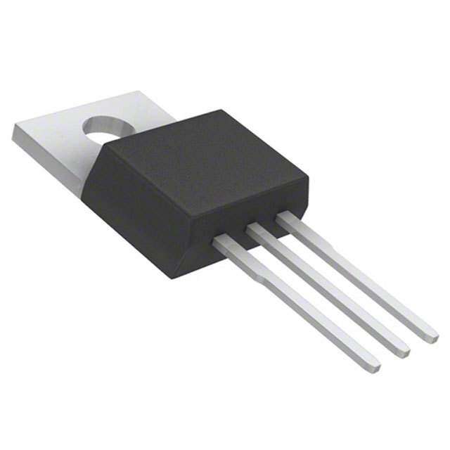
| 描述 | IC REG LDO ADJ 1A TO220-3 |
| 产品分类 | |
| 品牌 | Diodes Incorporated |
| 数据手册 | |
| 产品图片 |
|
| 产品型号 | AP1117TL-U |
| PCN过时产品 | |
| rohs | 无铅 / 符合限制有害物质指令(RoHS)规范要求 |
| RoHS指令信息 | http://diodes.com/download/4349 |
| 产品系列 | - |
| 产品目录页面 | |
| 供应商器件封装 | TO-220-3 |
| 其它名称 | AP1117TL-UDI |
| 包装 | 管件 |
| 安装类型 | 通孔 |
| 封装/外壳 | TO-220-3 |
| 工作温度 | 0°C ~ 125°C |
| 标准包装 | 1,000 |
| 电压-跌落(典型值) | 1.3V @ 1A |
| 电压-输入 | 6.4 V ~ 18 V |
| 电压-输出 | 1.25 V ~ 5 V |
| 电流-输出 | 1A |
| 电流-限制(最小值) | 1.1A |
| 稳压器拓扑 | 正,可调式 |
| 稳压器数 | 1 |


- 商务部:美国ITC正式对集成电路等产品启动337调查
- 曝三星4nm工艺存在良率问题 高通将骁龙8 Gen1或转产台积电
- 太阳诱电将投资9.5亿元在常州建新厂生产MLCC 预计2023年完工
- 英特尔发布欧洲新工厂建设计划 深化IDM 2.0 战略
- 台积电先进制程称霸业界 有大客户加持明年业绩稳了
- 达到5530亿美元!SIA预计今年全球半导体销售额将创下新高
- 英特尔拟将自动驾驶子公司Mobileye上市 估值或超500亿美元
- 三星加码芯片和SET,合并消费电子和移动部门,撤换高东真等 CEO
- 三星电子宣布重大人事变动 还合并消费电子和移动部门
- 海关总署:前11个月进口集成电路产品价值2.52万亿元 增长14.8%


PDF Datasheet 数据手册内容提取
AP1117 1A LOW DROPOUT POSITIVE ADJUSTABLE OR FIXED-MODE REGULATOR Features General Description • 1.4V Maximum Dropout at Full Load Current AP1117 is a low dropout positive adjustable or fixed-mode • Fast Transient Response regulator with 1A output current capability. The product is voltage • Output Current Limiting specifically designed to provide well-regulated supply for low • Built-in Thermal Shutdown IC applications such as high-speed bus termination and low • Good Noise Rejection current 3.3V logic supply. AP1117 is also well suited for other applications such as VGA cards. AP1117 is guaranteed to have • 3-Terminal Adjustable or Fixed 1.5V, 1.8V, 2.5V, 3.3V, 5.0V lower than 1.4V dropout at full load current making it ideal to provide well-regulated outputs of 1.25 to 5.0 with 6.4V to • Lead Free Packages: SOT223-3L, TO252-3L, 18V input supply. AP1117 is available in commercial temperature SOT89-3L, TO263-3L and TO220-3L grade. • SOT223-3L, TO252-3L, SOT89-3L, TO263-3L and TO220-3L: Available in “Green” Molding Compound (No Br, Sb) • Lead Free Finish/RoHS Compliant (Note 1) Applications • PC Peripheral • Communication Typical Application Circuit 5V 5V C1 C1 10uF 10uF VIN VIN V VOUT 3.3V/1A VOUT o 2.5V/1A R1 C2 121Ω C2 GND 22uF Adj R2 22uF 121Ω Tab is VOUT Tab is VOUT ( 5V/3.3V fixed output ) ( 5V/2.5V ADJ output ) R Note: V = V × (1+ 2) o REF R 1 AP1117 Rev. 19 1 of 12 JANUARY 2010 DS31009 www.diodes.com © Diodes Incorporated
AP1117 1A LOW DROPOUT POSITIVE ADJUSTABLE OR FIXED-MODE REGULATOR Ordering Information A P 1 1 1 7 X XXX -X Package Vout Lead Free Packing D : TO252-3L Blank : Adj L : Lead Free U : Tube E : SOT223-3L 15 : 1.5V G : Green 13 : Tape & Reel K : TO263-3L 18 : 1.8V T : TO220-3L 25 : 2.5V Y : SOT89-3L 33 : 3.3V 50 : 5.0V Tube 13” Tape and Reel Package Packaging Part Number Part Number Device Code (Note 2) Quantity Quantity Suffix Suffix AP1117DXXL-13 D TO252-3L NA NA 2500/Tape & Reel -13 AP1117DXXG-13 D TO252-3L NA NA 2500/Tape & Reel -13 AP1117EXXL-13 E SOT223-3L NA NA 2500/Tape & Reel -13 AP1117EXXG-13 E SOT223-3L NA NA 2500/Tape & Reel -13 AP1117KXXL-13 K TO263-3L NA NA 800/Tape & Reel -13 AP1117KXXG-13 K TO263-3L NA NA 800/Tape & Reel -13 AP1117TXXL-U T TO220-3L 50 -U NA NA AP1117TXXG-U T TO220-3L 50 -U NA NA AP1117YXXL-13 Y SOT89-3L NA NA 2500/Tape & Reel -13 AP1117YXXG-13 Y SOT89-3L NA NA 2500/Tape & Reel -13 Notes: 1. EU Directive 2002/95/EC (RoHS). All applicable RoHS exemptions applied. Please visit our website at http://www.diodes.com/products/lead_free.html. 2. Pad layout as shown on Diodes Inc. suggested pad layout document AP02001, which can be found on our website at http://www.diodes.com/datasheets/ap02001.pdf. AP1117 Rev. 19 2 of 12 JANUARY 2010 DS31009 www.diodes.com © Diodes Incorporated
AP1117 1A LOW DROPOUT POSITIVE ADJUSTABLE OR FIXED-MODE REGULATOR Pin Assignments (1) SOT89-3L (2) SOT223-3L ( Top View ) ( Top View ) 3 VIN 3 VIN 2 VOUT 2 VOUT 1 Adj (GND) 1 Adj (GND) Tab is VOUT Tab is VOUT (3) TO220-3L (4) TO252-3L and TO263-3L ( Top View ) ( Front View ) 3 VIN 3 V IN 2 V 2 VOUT OUT 1 Adj (GND) 1 Adj (GND) Tab is VOUT Tab is VOUT Pin Descriptions Pin Name I/O PIN # Description A resistor divider from this pin to the V pin and ground sets the output Adj (GND) I 1 OUT voltage (Ground only for Fixed-Mode). The output of the regulator. A minimum of 10uF capacitor (0.15Ω ≤ ESR ≤ V O 2 OUT 20Ω) must be connected from this pin to ground to insure stability. The input pin of regulator. Typically a large storage capacitor is connected from this pin to ground to insure that the input voltage does not sag below V I 3 the minimum dropout voltage during the load transient response. This pin IN must always be 1.3V higher than V in order for the device to regulate OUT properly. AP1117 Rev. 19 3 of 12 JANUARY 2010 DS31009 www.diodes.com © Diodes Incorporated
AP1117 1A LOW DROPOUT POSITIVE ADJUSTABLE OR FIXED-MODE REGULATOR Block Diagram V 3 2 V IN OUT + + + - 1.25V CURRENT 1 LIMIT GND + (FIXED) Thermal Shutdown - 1 Adj Absolute Maximum Ratings Symbol Parameter Rating Unit V DC Supply Voltage -0.3 to 18 V IN TMJ Maximum Junction Temperature 150 oC Power Dissipation SOT89-3L Internally limited by maximum SOT223-3L P junction temperature mW D TO220-3L of 150 oC (Note 3) TO252-3L TO263-3L TST Storage Temperature -65 to +150 oC Notes: 3. AP1117 contains an internal thermal limiting circuit that is designed to protect the regulator in the event that the maximum junction temperature exceeded. When activated, typically at 150°C, the regulator output switches off and then back on as the die cools. Recommended Operating Conditions Symbol Parameter Min Max Unit TOP Operating Junction Temperature Range 0 125 oC AP1117 Rev. 19 4 of 12 JANUARY 2010 DS31009 www.diodes.com © Diodes Incorporated
AP1117 1A LOW DROPOUT POSITIVE ADJUSTABLE OR FIXED-MODE REGULATOR Electrical Characteristics (Under Operating Conditions) Parameter Conditions Min Typ. Max Unit Reference Voltage AP1117-ADJ TA = 25oC, (VIN-OUT) = 1.5V 1.225 1.250 1.275 V IO = 10mA AP1117-1.5 IOUT = 10mA, TA = 25oC, 1.470 1.500 1.530 V 3V≦VIN≦12V AP1117-1.8 IOUT = 10mA, TA = 25oC, 1.764 1.800 1.836 V 3.3V≦VIN≦12V Output Voltage AP1117-2.5 IOUT = 10mA, TA = 25oC, 2.450 2.500 2.550 V 4V≦VIN≦12V AP1117-3.3 IOUT = 10mA, TA = 25oC, 3.235 3.300 3.365 V 4.8V≦VIN≦12V AP1117-5.0 IOUT = 10mA, TA = 25oC, 4.900 5.000 5.100 V 6.5V≦VIN≦12V Line Regulation AP1117-XXX IO = 10mA,VOUT+1.5V<VIN<12V, 0.2 % TA = 25oC AP1117-ADJ VIN=3.3V,Vadj=0,0mA<Io<1A, 1 % TA = 25oC (Note 4, 5) AP1117-1.5 VIN = 3V, 0mA<Io<1A, 12 15 mV TA = 25oC (Note 4, 5) AP1117-1.8 VIN = 3.3V, 0mA<Io<1A, 15 18 mV TA = 25oC (Note 4, 5) Load Regulation AP1117-2.5 VIN = 4V, 0mA<Io<1A, 20 25 mV TA = 25oC (Note 4, 5) AP1117-3.3 VIN = 5V, 0≦IOUT≦1A, 26 33 mV TA= 25oC (Note 4, 5) AP1117-5.0 VIN = 8V, 0≦IOUT≦1A, 40 50 mV TA = 25oC (Note 4, 5) Dropout Voltage AP1117-ADJ/1.5/1.8 (VIN-VOUT) /2.5/3.3/5.0 IOUT = 1A, ΔVOUT = 1%VOUT 1.3 1.4 V AP1117-ADJ/1.5/1.8 Current Limit /2.5/3.3/5.0 (VIN-VOUT) = 5V 1. 1 A M(Ninotime u6m) Load Current AP1117-XXX 0oC≦TJ≦125oC 5 10 mA Thermal Regulation TA = 25oC, 30ms pulse 0.008 0.04 %/W Ripple Rejection F = 180Hz, COUT = 25uF Tantalum, IOUT = 1A AP1117-XXX VIN = VOUT+3V 60 70 dB Temperature Stability IO = 10mA 0.5 % SOT89-3L: Control Circuitry/Power Transistor (Note 7) 164 θJAThermal Resistance STOO2T5222-33-L3:L C: Conotnrotrlo Cl Circiruciutriytr/yP/oPwowere Tr rTarnasnissitsotro (rN (Notoet e7 )8 ) 17037 oC /W Junction-to-Ambient TO220-3L: Control Circuitry/Power Transistor (Note 7) 78 TO263-3L: Control Circuitry/Power Transistor (Note 7) 60 SOT89-3L: Control Circuitry/Power Transistor (Note 7) 42 θJCThermal Resistance STOO2T5222-33-L3:L C: Conotnrotrlo Cl Circiruciutriytr/yP/oPwowere Tr rTarnasnissitsotro (rN (Notoet e7 )8 ) 1152 oC /W Junction-to-Case TO220-3L: Control Circuitry/Power Transistor (Note 7) 3.5 TO263-3L: Control Circuitry/Power Transistor (Note 7) 3.5 Notes: 4. See thermal regulation specifications for changes in output voltage due to heating effects. Line and load regulation are measured at a constant junction temperature by low duty cycle pulse testing. Load regulation is measured at the output lead = 1/18” from the package. 5. Line and load regulation are guaranteed up to the maximum power dissipation of 15W. Power dissipation is determined by the difference between input and output differential and the output current. Guaranteed maximum power dissipation will not be available over the full input/output range. 6. Quiescent current is defined as the minimum output current required in maintaining regulation. At 12V input/output differential the device is guaranteed to regulate if the output current is greater than 10mA. 7. Test conditions for SOT89-3L, TO220-3L, TO252-3L and TO263-3L: Devices mounted on FR-4 substrate, single sided PC board, 2oz copper, with minimum recommended pad layout, no air flow. The case point of θJC is located on the thermal tab. 8. Test conditions for SOT223-3L: Devices mounted on FR-4 substrate, single sided PC board, 2oz copper, with 5mmx5mm thermal pad layout, no air flow. The case point of θJC is located on the thermal tab. AP1117 Rev. 19 5 of 12 JANUARY 2010 DS31009 www.diodes.com © Diodes Incorporated
AP1117 1A LOW DROPOUT POSITIVE ADJUSTABLE OR FIXED-MODE REGULATOR Typical Performance Characteristics 2. 0 0.20 1. 8 %) 1. 6 n ( 0 I load=800mA V)1. 4 atio e (1. 2 Tj = 25 oC evi-0.20 g D olta1. 0 ge V a opout 00.. 68 Tj = 125 oC ut Volt-0.40 Dr0. 4 Outp-0.80 0. 2 0 - 1 0 250 500 750 1000 -40 0 25 50 75 100 125 Output Current (mA) Temperature (oC) Dropout Voltage vs Output Current Load Regulation vs Temperature 2 1 1.5 0.8 1 %) hange (00. 5 ation (%)0.6 e C evi oltag-0.5 ge D0.4 utput V--1 .15 ut Volta0.2 O p ut - 2 O 0 -40 -25 0 25 50 75 100 125 150 2 4 6 8 10 12 Temperature (oC) Input Voltage (V) Percent Change in Output Voltage vs Temperature Line Regulation ut Voltage (V) 567...555 CCoinu=t1=u1F0uF Tantalum eviation (mV)123000 CCPr oienul o=ta =1d u1=F0 1 u0F0 m TAantalum p D 0 In 40 ge mV) Volta-10 n ( 20 ut -20 o p ati ut evi 0 O 2 age D -20 nt (A) 1 Volt urre 0 Output -400 20 40 6T0IME80 (us1)00 120 140 160 180 200 Load C -10 10 20 30 T4I0ME 5(u0s)60 70 80 90 100 Line Transient Response Load Transient Response AP1117 Rev. 19 6 of 12 JANUARY 2010 DS31009 www.diodes.com © Diodes Incorporated
AP1117 1A LOW DROPOUT POSITIVE ADJUSTABLE OR FIXED-MODE REGULATOR Marking Information (1) SOT223-3L ( Top View ) Y : Year : 0~9 Logo Y W X W : Week : A~Z : 1~26 week; Part Number a~z : 27~52 week; z repersents 52 and 53 week 1117 for ADJ 1 7-VV X : Internal code 17-VV:15 for 1.5V a~z : Lead Free 18 for 1.8V A~Z : Green 25 for 2.5V 33 for 3.3V 50 for 5.0V (2) TO252-3L ( Top View ) Logo L : Lead Free G : Green Part Number 17-VV YY : Year : 01~09 1117 for ADJ YY WW X X 17-VV:15 for 1.5V WW : Week : 01~52, 52 represents 18 for 1.8V 52 and 53 week 25 for 2.5V X : Internal Code 33 for 3.3V 50 for 5.0V AP1117 Rev. 19 7 of 12 JANUARY 2010 DS31009 www.diodes.com © Diodes Incorporated
AP1117 1A LOW DROPOUT POSITIVE ADJUSTABLE OR FIXED-MODE REGULATOR Marking Information (Continued) (3) SOT89-3L ( Top View ) XX : Identification code Y : Year : 0~9 X X W : Week : A~Z : 1~26 week; Y W X a~z : 27~52 week; z represents 52 and 53 week X : Internal code 1 2 3 a~z : Lead Free A~Z : Green Marking Code Table Identification Code Output Version DA AP1117-ADJ DB AP1117-1.5V DC AP1117-1.8V DD AP1117-2.5V DE AP1117-3.3V DF AP1117-5.0V (4) TO263-3L ( Top View ) Logo L : Lead Free G : Green Part Number 1117-VV YY : Year : 01~09 VV: 15 for 1.5V YY WW X X WW : Week : 01~52, 52 represents 18 for 1.8V 52 and 53 week 25 for 2.5V X : Internal code 33 for 3.3V 50 for 5.0V Blank for ADJ AP1117 Rev. 19 8 of 12 JANUARY 2010 DS31009 www.diodes.com © Diodes Incorporated
AP1117 1A LOW DROPOUT POSITIVE ADJUSTABLE OR FIXED-MODE REGULATOR Marking Information (Continued) (5) TO220-3L ( Top View ) Logo L : Lead Free G : Green Part Number 17 - VV YY : Year : 01~09 1117 for ADJ YYWWXX 17-VV : 15 for 1.5V WW : Week : 01~52, 52 represents 18 for 1.8V 52 and 53 week 25 for 2.5V X : Internal code 33 for 3.3V 50 for 5.0V Package Information (All Dimensions in mm) (1) Package Type: SOT223-3L AP1117 Rev. 19 9 of 12 JANUARY 2010 DS31009 www.diodes.com © Diodes Incorporated
AP1117 1A LOW DROPOUT POSITIVE ADJUSTABLE OR FIXED-MODE REGULATOR Package Information (Continued) (2) Package Type: TO252-3L 7 2 5.6 1. 6.354/6.80 Typ 6.58 8/ 8 5.20/5.50 Typ 5.35 0. 6 5. 0/6.20p 5.57 11.0 7.2 4y 5.T 2.25 0 2. 1.2 0.61 Typ 2.28 Land Pattern Recommendation (Unit: mm) 0.64/1.02 BSC. 2.18/2.40 4.57 BSC. Typ 0.83 01..8194/ 9.00/10.40 Typ 9.70 Typ 2.29 2 E 0.45/0.58 0.51 OT SEATING Typ 0.52 E N PLANE 0T.y4p5 /00..5528 E S (3) Package Type: SOT89-3L 1.40/1.75 Typ 1.60 1.7 8 4 2. Typ 5 2.7 35/2.60 3.94/4.2 2. 0.4 9 0.80/1.20 1. 1.3 1.45/1.55 Typ 1.50 0.9 1.5 2.90/3.10 Land Pattern Recommendation (Unit: mm) Typ 3.00 50(2x) 80(2x) 4.40/4.60 Typ 4.50 00 0/1.6p 1.5 1.4Ty 0.36/0.480.41/0.530.36/0.48 0.35/0.43 Typ 0.42 Typ 0.47 Typ 0.42 Typ 0.39 AP1117 Rev. 19 10 of 12 JANUARY 2010 DS31009 www.diodes.com © Diodes Incorporated
AP1117 1A LOW DROPOUT POSITIVE ADJUSTABLE OR FIXED-MODE REGULATOR Package Information (Continued) (4) Package Type: TO263-3L 0 9.65/10.29 Typ 9.97 2.92Typ 1.3 10.9 5 4 Typ 9.1 yp 15.2 9.1 65 8 T 5.7 8.65/9. 61/15.8 1 4. 1 3 2.54 1.27/1.78Typ 1.52 1.3 2.54 BSC. 0.51/0.99 Typ 0.75 Land Pattern Recommendation (Unit: mm) 1.14/1.40 Typ1.27 0.38 Typ 4.06/4.83Typ 4.45 2.28/2.80 Typ 2.54 1.14/1.40Typ 1.27 (5) Package Type: TO220-3L 3.55/4.85 2.54/3.43 9.70/10.70 Ø3.53/4.09 Typ 4.20 0.51/1.40 Typ 2.98 Typ 10.20 Typ 3.81 Typ 0.95 E 5.84/6.86 N A 14.20/16.50Typ 15.35 Typ 6.35 SEATING PL 3.66/6.35 Typ 5.00 1T.1y4p/ 11..4768 2.72/14.72Typ 13.72 1 0.31/1.14 0.51/1.14 Typ 0.72 Typ 0.83 2.99/2.79 2.03/2.92 4.83/5.33 Typ 2.54 Typ2.48 Typ 5.08 AP1117 Rev. 19 11 of 12 JANUARY 2010 DS31009 www.diodes.com © Diodes Incorporated
AP1117 1A LOW DROPOUT POSITIVE ADJUSTABLE OR FIXED-MODE REGULATOR IMPORTANT NOTICE DIODES INCORPORATED MAKES NO WARRANTY OF ANY KIND, EXPRESS OR IMPLIED, WITH REGARDS TO THIS DOCUMENT, INCLUDING, BUT NOT LIMITED TO, THE IMPLIED WARRANTIES OF MERCHANTABILITY AND FITNESS FOR A PARTICULAR PURPOSE (AND THEIR EQUIVALENTS UNDER THE LAWS OF ANY JURISDICTION). Diodes Incorporated and its subsidiaries reserve the right to make modifications, enhancements, improvements, corrections or other changes without further notice to this document and any product described herein. Diodes Incorporated does not assume any liability arising out of the application or use of this document or any product described herein; neither does Diodes Incorporated convey any license under its patent or trademark rights, nor the rights of others. Any Customer or user of this document or products described herein in such applications shall assume all risks of such use and will agree to hold Diodes Incorporated and all the companies whose products are represented on Diodes Incorporated website, harmless against all damages. Diodes Incorporated does not warrant or accept any liability whatsoever in respect of any products purchased through unauthorized sales channel. Should Customers purchase or use Diodes Incorporated products for any unintended or unauthorized application, Customers shall indemnify and hold Diodes Incorporated and its representatives harmless against all claims, damages, expenses, and attorney fees arising out of, directly or indirectly, any claim of personal injury or death associated with such unintended or unauthorized application. Products described herein may be covered by one or more United States, international or foreign patents pending. Product names and markings noted herein may also be covered by one or more United States, international or foreign trademarks. LIFE SUPPORT Diodes Incorporated products are specifically not authorized for use as critical components in life support devices or systems without the express written approval of the Chief Executive Officer of Diodes Incorporated. As used herein: A. Life support devices or systems are devices or systems which: 1. are intended to implant into the body, or 2. support or sustain life and whose failure to perform when properly used in accordance with instructions for use provided in the labeling can be reasonably expected to result in significant injury to the user. B. A critical component is any component in a life support device or system whose failure to perform can be reasonably expected to cause the failure of the life support device or to affect its safety or effectiveness. Customers represent that they have all necessary expertise in the safety and regulatory ramifications of their life support devices or systems, and acknowledge and agree that they are solely responsible for all legal, regulatory and safety-related requirements concerning their products and any use of Diodes Incorporated products in such safety-critical, life support devices or systems, notwithstanding any devices- or systems-related information or support that may be provided by Diodes Incorporated. Further, Customers must fully indemnify Diodes Incorporated and its representatives against any damages arising out of the use of Diodes Incorporated products in such safety-critical, life support devices or systems. Copyright © 2009, Diodes Incorporated www.diodes.com AP1117 Rev. 19 12 of 12 JANUARY 2010 DS31009 www.diodes.com © Diodes Incorporated