ICGOO在线商城 > 集成电路(IC) > PMIC - 稳压器 - DC DC 开关稳压器 > AOZ1281DI
 Datasheet下载
- 型号: AOZ1281DI
- 制造商: ALPHA&OMEGA
- 库位|库存: xxxx|xxxx
- 要求:
| 数量阶梯 | 香港交货 | 国内含税 |
| +xxxx | $xxxx | ¥xxxx |
查看当月历史价格
查看今年历史价格
AOZ1281DI产品简介:
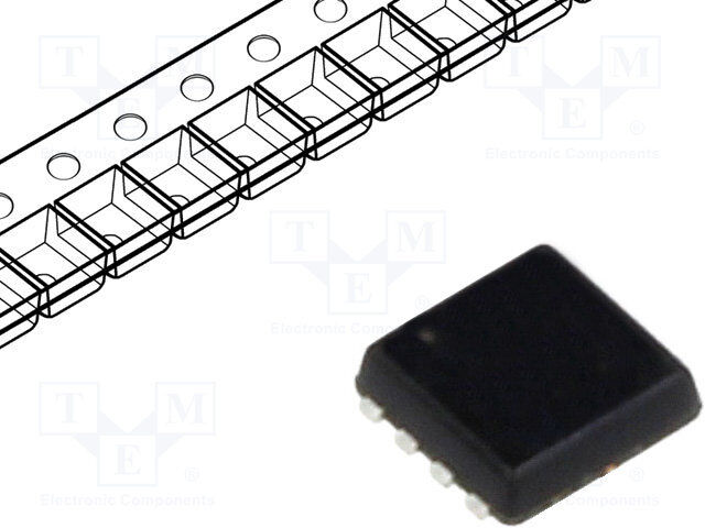
ICGOO电子元器件商城为您提供AOZ1281DI由ALPHA&OMEGA设计生产,在icgoo商城现货销售,并且可以通过原厂、代理商等渠道进行代购。 AOZ1281DI价格参考。ALPHA&OMEGAAOZ1281DI封装/规格:PMIC - 稳压器 - DC DC 开关稳压器, 可调式 降压 开关稳压器 IC 正 0.8V 1 输出 1.8A 8-WFDFN 裸露焊盘。您可以下载AOZ1281DI参考资料、Datasheet数据手册功能说明书,资料中有AOZ1281DI 详细功能的应用电路图电压和使用方法及教程。
| 参数 | 数值 |
| 产品目录 | 集成电路 (IC) |
| 描述 | IC REG BUCK ADJ 1.8A 8DFN |
| 产品分类 | |
| 品牌 | Alpha & Omega Semiconductor Inc |
| 数据手册 | |
| 产品图片 |
|
| 产品型号 | AOZ1281DI |
| PWM类型 | 电流模式 |
| rohs | 无铅 / 符合限制有害物质指令(RoHS)规范要求 |
| 产品系列 | EZBuck™ |
| 供应商器件封装 | 8-DFN(2x2) |
| 其它名称 | 785-1276-1 |
| 包装 | 剪切带 (CT) |
| 同步整流器 | 无 |
| 安装类型 | 表面贴装 |
| 封装/外壳 | 8-WFDFN 裸露焊盘 |
| 工作温度 | -40°C ~ 85°C |
| 标准包装 | 1 |
| 电压-输入 | 3 V ~ 26 V |
| 电压-输出 | 0.8 V ~ 22.1 V |
| 电流-输出 | 1.8A |
| 类型 | 降压(降压) |
| 输出数 | 1 |
| 输出类型 | 可调式 |
| 频率-开关 | 1.5MHz |
.jpg)


- 商务部:美国ITC正式对集成电路等产品启动337调查
- 曝三星4nm工艺存在良率问题 高通将骁龙8 Gen1或转产台积电
- 太阳诱电将投资9.5亿元在常州建新厂生产MLCC 预计2023年完工
- 英特尔发布欧洲新工厂建设计划 深化IDM 2.0 战略
- 台积电先进制程称霸业界 有大客户加持明年业绩稳了
- 达到5530亿美元!SIA预计今年全球半导体销售额将创下新高
- 英特尔拟将自动驾驶子公司Mobileye上市 估值或超500亿美元
- 三星加码芯片和SET,合并消费电子和移动部门,撤换高东真等 CEO
- 三星电子宣布重大人事变动 还合并消费电子和移动部门
- 海关总署:前11个月进口集成电路产品价值2.52万亿元 增长14.8%


PDF Datasheet 数据手册内容提取
AOZ1281 EZBuck™ 1.8 A Simple Buck Regulator General Description Features The AOZ1281 is a high efficiency, simple to use, 1.8 A (cid:122) 3 V to 26 V operating input voltage range buck regulator flexible enough to be optimized for a (cid:122) 240 mΩ internal NMOS variety of applications. The AOZ1281 works from a 3 V to (cid:122) High efficiency: up to 95 % 26 V input voltage range, and provides up to 1.8 A of continuous output current. The output voltage is (cid:122) Internal compensation adjustable down to 0.8 V. The fixed switching frequency (cid:122) 1.8 A continuous output current of 1.5 MHz PWM operation reduces inductor size. (cid:122) Fixed 1.5 MHz PWM operation (cid:122) Internal soft start (cid:122) Output voltage adjustable down to 0.8 V (cid:122) Cycle-by-cycle current limit (cid:122) Short-circuit protection (cid:122) Thermal shutdown (cid:122) Small size: DFN 2x2, 8L Applications (cid:122) Point of load DC/DC conversion (cid:122) Set top boxes (cid:122) DVD drives and HDD (cid:122) LCD Monitors & TVs (cid:122) Cable modems (cid:122) Telecom/Networking/Datacom equipment Typical Application VIN C3 C1 4.7µF BST L1 2.2µH EN VOUT LX AOZ1281 R1 C2 FB 10µF GND R2 Figure 1. 1.8 A Buck Regulator Rev. 1.0 June 2011 www.aosmd.com Page 1 of 12
AOZ1281 Ordering Information Part Number Ambient Temperature Range Package Environmental AOZ1281DI -40 °C to +85 °C DFN 2 x 2, 8L Green Product AOS Green Products use reduced levels of Halogens, and are also RoHS compliant. Please visit www.aosmd.com/web/quality/rohs_compliant.jsp for additional information. Pin Configuration LX 1 8 BST VIN 2 7 GND Exposed Pad VIN 3 6 GND EN 4 5 FB DFN 2x2, 8L (Top View) Pin Description Pin Number Pin Name Pin Function 1 LX PWM output connection to inductor. 2, 3 VIN Supply voltage input. Range from 3 V to 26 V. When VIN rises above the UVLO threshold the device starts up. If Vin is lower than 4.5 V, an external 5 V is needed to add through the external diode for BST. 4 EN Enable pin. The enable pin is active high. Connect EN pin to VIN through current limiting resistor. Do not leave the EN pin floating. 5 FB Feedback input. It is regulated to 0.8 V. The FB pin is used to determine the PWM output voltage via a resistor divider between the output and GND. 6, 7 GND Ground. 8 BST Bootstrap voltage input. High side driver supply. Connected to 10 nF capacitor between BST and LX. Exposed Pad Thermal exposed pad. Pad can be connected to GND if necessary for improved thermal performance. Rev. 1.0 June 2011 www.aosmd.com Page 2 of 12
AOZ1281 Absolute Maximum Ratings Recommended Operating Conditions Exceeding the Absolute Maximum Ratings may damage the The device is not guaranteed to operate beyond the device. Recommended Operating Conditions. Parameter Rating Parameter Rating Supply Voltage (V ) 30 V Supply Voltage (V ) 3.0 V to 26 V IN VIN LX to GND -0.7 V to V +2 V Output Voltage Range 0.8 V to 0.85xV VIN VIN EN to GND -0.3 V to 26 V Ambient Temperature (T ) -40 °C to +85 °C A FB to GND -0.3 V to 6 V Package Thermal Resistance DFN 2x2, 8L (Θ )(2) 55 °C/W BST to GND V + 6 V JA LX Note: Junction Temperature (T ) +150 °C J 2. The value of Θ is measured with the device mounted on a 1-in2 JA Storage Temperature (TS) -65 °C to +150 °C FR-4 board with 2 oz. Copper, in a still air environment with ESD Rating(1) 2 kV TA = 25 °C. The value in any given application depends on the user’s specific board design. Note: 1. Devices are inherently ESD sensitive, handling precautions are required. Human body model rating: 1.5 kΩ in series with 100 pF. Electrical Characteristics T = 25 °C, V = V = 12 V. Specifications in BOLD indicate a temperature range of -40 °C to +85 °C. These specifications are A VIN EN guaranteed by design. Symbol Parameter Conditions Min. Typ. Max. Units V Supply Voltage 3 26 V VIN V Input Under-Voltage Lockout Threshold V Rising 2.9 V UVLO VIN V Falling 2.3 V VIN UVLO Hysteresis 200 mV I Supply Current (Quiescent) I = 0, V = 1 V, V > 1.2 V 1 1.5 mA VIN OUT FB EN I Shutdown Supply Current V = 0 V 8 μA OFF EN V Feedback Voltage T = 25 ºC 784 800 816 mV FB A V Load Regulation 120 mA < Load < 1.08 A 0.5 % FB_LOAD V Line Regulation Load = 600 mA 0.03 % / V FB_LINE I Feedback Voltage Input Current V = 800 mV 500 nA FB FB ENABLE V EN Input Threshold Off Threshold 0.4 V EN_OFF V On Threshold 1.2 V EN_ON V EN Input Hysteresis 200 mV EN_HYS I Enable Input Current 3 μA EN MODULATOR f Frequency 1.2 1.5 1.8 MHz O D Maximum Duty Cycle 87 % MAX T Minimum On Time 100 ns ON_MIN I Current Limit 2.2 2.6 A LIM Over-Temperature Shutdown Limit T Rising 150 °C J T Falling 110 °C J T Soft Start Interval 400 μs SS POWER STATE OUTPUT R NMOS On-Resistance V = 12 V 240 mΩ DS(ON) IN V = 3.3 V 380 mΩ IN I NMOS Leakage V = 0 V, V = 0 V 10 μA LEAKAGE EN LX Rev. 1.0 June 2011 www.aosmd.com Page 3 of 12
AOZ1281 Block Diagram VIN Regulator + Current Sense EN Enable Softstart BST BST Detect LDO Ramp OC Generator CLK OSC PWM FB – Logic – Driver 0.8V + Error + LX Amplifier PWM Comparator GND Rev. 1.0 June 2011 www.aosmd.com Page 4 of 12
AOZ1281 Typical Performance Characteristics Circuit of Figure 1. V = 12 V, V = 3.3 V, L = 4.7 μH, C1 = 10 μF, C2 = 22 μF, T = 25 °C, unless otherwise specified. IN OUT A Light Load Operaiton Full Load Operation Vin Vin 50mV/div 200mV/div Vo Vo 20mV/div 20mV/div IL IL 500mA/div 1A/div Vlx Vlx 5V/div 5V/div 500ns/div 500ns/div Startup to Full Load Short Circuit Protection Vo 1V/div Vin 5V/div Vin 5V/div Vlx 5V/div Iin 1A/div Vo 1V/div lL 1A/div 2ms/div 2ms/div 50% to 100% Load Transient Short Circuit Recovery Vin 5V/div Vlx Vo 5V/div 50mV/div Vo 1V/div Io lL 1A/div 1A/div 200μs/div 2ms/div Rev. 1.0 June 2011 www.aosmd.com Page 5 of 12
AOZ1281 Efficiency Efficiency (V = 12V) vs. Load Current IN 95 90 85 %) y ( 80 c n e ci 75 ffi E 70 5.0V OUTPUT 65 3.3V OUTPUT 1.8V OUTPUT 1.2V OUTPUT 60 0 0.2 0.4 0.6 0.8 1.0 1.2 1.4 1.6 1.8 Load Current (A) Detailed Description The AOZ1281 is a current-mode step down regulator Steady-State Operation with integrated high side NMOS switch. It operates from Under steady-state conditions, the converter operates a 3 V to 26 V input voltage range and supplies up to 1.8 A infixed frequency and Continuous-Conduction Mode of load current. Features include: enable control, under (CCM). voltage lock-out, internal soft-start, output over-voltage protection, over-current protection, and thermal shut The AOZ1281 integrates an internal NMOS as the down. The AOZ1281 is available in a DFN 2x2, 8L high-side switch. Inductor current is sensed by amplifying package. the voltage drop across the drain to the source of the high-side power MOSFET. Output voltage is divided Enable and Soft Start down by the external voltage divider at the FB pin. The AOZ1281 has an internal soft start feature to limit Thedifference of the FB pin voltage and reference in-rush current and ensure the output voltage ramps up voltage is amplified by the internal transconductance smoothly to regulation voltage. A soft start process error amplifier. The error voltage is compared against begins when the input voltage rises to a voltage higher the current signal, which is sum of inductor current signal than UVLO and the voltage level on the EN pin is HIGH. plus ramp compensation signal, at the PWM comparator In the soft start process, the output voltage is typically input. If the current signal is less than the error voltage, ramped to regulation voltage in 400 μs. The 400 μs the internal high-side switch is on. The inductor current softstart time is set internally. flows from the input through the inductor to the output. When the current signal exceeds the error voltage, the The EN pin of the AOZ1281 is active high. Connect the high-side switch is off. The inductor current is EN pin to VIN if the enable function is not used. Pulling freewheeling through the external Schottky diode to EN to ground will disable the AOZ1281. Do not leave EN output. open. The voltage on the EN pin must be above 1.2 V to enable the AOZ1281. When voltage on the EN pin falls Switching Frequency below 0.4 V, the AOZ1281 is disabled. The AOZ1281 switching frequency is fixed and set by an internal oscillator. The switching frequency is set internally 1.5 MHz. Rev. 1.0 June 2011 www.aosmd.com Page 6 of 12
AOZ1281 Output Voltage Programming The converter will start up via a soft start once the short circuit condition is resolved. In the short circuit protection Output voltage can be set by feeding back the output to mode, the inductor average current is greatly reduced. the FB pin with a resistor divider network. Refer to the application circuit shown in Figure 1. The resistor divider Under Voltage Lock Out (UVLO) network includes R and R . Usually, a design is started 1 2 by picking a fixed R value and calculating the required An UVLO circuit monitors the input voltage. When the 2 R with equation below. input voltage exceeds 2.9 V, the converter starts 1 operation. When input voltage falls below 2.3 V, the ⎛ R1⎞ converter will stop switching. V = 0.8×⎜1+-------⎟ O ⎝ R ⎠ 2 Thermal Protection An internal temperature sensor monitors the junction Some standard values of R and R for the most 1 2 temperature. The sensor shuts down the internal control commonly used output voltage values are listed in circuit and high side NMOS if the junction temperature Table1. exceeds 150 °C. The regulator will restart automatically Table 1. under the control of the soft-start circuit when the junction temperature decreases to 100 °C. V (V) R (kΩ) R (kΩ) O 1 2 Application Information 1.8 80.6 64.2 2.5 49.9 23.4 The basic AOZ1281 application circuit is shown in Figure1. Component selection is explained below. 3.3 49.9 15.8 5.0 49.9 9.53 Input Capacitor The input capacitor must be connected to the VIN pin The combination of R and R should be large enough to 1 2 and the GND pins of the AOZ1281 to maintain steady avoid drawing excessive current from the output, which input voltage and filter out the pulsing input current. The will cause power loss. voltage rating of the input capacitor must be greater than maximum input voltage plus ripple voltage. Protection Features The input ripple voltage can be approximated by the The AOZ1281 has multiple protection features to prevent equation below: system circuit damage under abnormal conditions. I ⎛ V ⎞ V Over Current Protection (OCP) ΔV = --------O--------- ×⎜1–-----O----⎟ ×-----O---- IN The sensed inductor current signal is also used for over f×CIN ⎝ VIN⎠ VIN current protection. Since the input current is discontinuous in a buck The cycle-by-cycle current limit threshold is set to 2 A. converter, the current stress on the input capacitor is When the load current reaches the current limit another concern when selecting the capacitor. For a threshold, the cycle-by-cycle current limit circuit buckcircuit, the RMS value of input capacitor current can immediately turns off the high-side switch to terminate be calculated by: the current duty cycle. The inductor current stop rising. Thecycle-by-cycle current limit protection directly limits V ⎛ V ⎞ inductor peak current. The average inductor current is I = I × -----O----⎜1–-----O----⎟ also limited due to the limitation on peak inductor current. CIN_RMS O V ⎝ V ⎠ IN IN When cycle-by-cycle current limit circuit is triggered, the output voltage drops as the duty cycle decreases. if we let m equal the conversion ratio: The AOZ1281 has internal short circuit protection to V O protect itself from catastrophic failure under output short --------- = m V circuit conditions. The FB pin voltage is proportional to IN the output voltage. Whenever the FB pin voltage is below 0.2 V, the short circuit protection circuit is triggered. As a result, the converter is shut down and hiccups. Rev. 1.0 June 2011 www.aosmd.com Page 7 of 12
AOZ1281 The relationship between the input capacitor RMS When selecting the inductor, confirm it is able to handle current and voltage conversion ratio is calculated and the peak current without saturation at the highest shown in Figure 2. It can be seen that when V is half of operating temperature. O V , C is under the worst current stress. The worst IN IN current stress on C is 0.5 x I . The inductor takes the highest current in a buck circuit. IN O The conduction loss on inductor needs to be checked for 0.5 thermal and efficiency requirements. 0.4 Surface mount inductors in different shape and styles are available from Coilcraft, Elytone and Murata. Shielded I (m) 0.3 inductors are small and radiate less EMI noise but cost CIN_RMS I more than unshielded inductors. The choice depends on O 0.2 EMI requirement, price and size. 0.1 Output Capacitor The output capacitor is selected based on the DC output 0 voltage rating, output ripple voltage specification and 0 0.5 1 ripple current rating. m Figure 2. I vs. Voltage Conversion Ratio The selected output capacitor must have a higher rated CIN voltage specification than the maximum desired output For reliable operation and best performance, the input voltage including ripple. De-rating needs to be capacitors must have a current rating higher than considered for long term reliability. I at the worst operating conditions. Ceramic CIN_RMS capacitors are preferred for use as input capacitors Output ripple voltage specification is another important because of their low ESR and high ripple current rating. factor for selecting the output capacitor. In a buck Depending on the application circuits, other low ESR converter circuit, output ripple voltage is determined by tantalum capacitors or aluminum electrolytic capacitors inductor value, switching frequency, output capacitor may be used. When selecting ceramic capacitors, value and ESR. It can be calculated by the equation X5R or X7R type dielectric ceramic capacitors are below: preferred for their better temperature and voltage ⎛ 1 ⎞ characteristics. ΔV = ΔI × ESR +------------------------- O L ⎝ CO ⎠ 8×f×C O Note that the ripple current rating from capacitor where, manufacturers is based on a fixed life time. Further de-rating may be necessary for practical design CO is output capacitor value, and requirements. ESR is the equivalent series resistance of the output CO capacitor. Inductor When a low ESR ceramic capacitor is used as the output The inductor is used to supply constant current to output capacitor, the impedance of the capacitor at the switching when it is driven by a switching voltage. For given input frequency dominates. Output ripple is mainly caused by and output voltage, inductance and switching frequency capacitor value and inductor ripple current. The output together decide the inductor ripple current, which is: ripple voltage calculation can be simplified to: ΔI = --V----O-----×⎜⎛1–-V----O----⎟⎞ ⎛ 1 ⎞ L f×L ⎝ VIN⎠ ΔVO = ΔIL×⎝-8----×-----f---×-----C-------⎠ O The peak inductor current is: If the impedance of ESR at switching frequency ΔI dominates, the output ripple voltage is mainly decided by L I = I +-------- capacitor ESR and inductor ripple current. The output Lpeak O 2 ripple voltage calculation can be further simplified to: High inductance provides a low inductor ripple current ΔV = ΔI ×ESR O L CO but requires larger size inductor to avoid saturation. Lowripple current reduces inductor core losses and also reduces RMS current through inductor and switches. This results in less conduction loss. Rev. 1.0 June 2011 www.aosmd.com Page 8 of 12
AOZ1281 For lower output ripple voltage across the entire The power dissipation in the Schottky diode can be operating temperature range, X5R or X7R dielectric type approximated as: of ceramic, or other low ESR tantalum capacitor or aluminum electrolytic capacitor may also be used as Pdiode_loss = IO ×(1–D)×VFW_Schottky output capacitors. where, In a buck converter, output capacitor current is V is the Schottky diode forward voltage drop. continuous. The RMS current of the output capacitor is FW_Schottky decided by the peak to peak inductor ripple current. The power dissipation of the inductor can be It can be calculated by: approximately calculated by output current and DCR of ΔI the inductor. L I = ---------- CO_RMS 12 P =I 2×R ×1.1 inductor_loss O inductor Usually, the ripple current rating of the output capacitor is The actual junction temperature can be calculated with a smaller issue because of the low current stress. When power dissipation in the AOZ1281 and thermal the buck inductor is selected to be very small and impedance from junction to ambient. inductor ripple current is high, the output capacitor could be overstressed. T junction = (P –P –P )×Θ Schottky Diode Selection total_loss diode_loss inductor_loss JA +T The external freewheeling diode supplies the current amb tothe inductor when the high side NMOS switch is off. Toreduce the losses due to the forward voltage drop and The maximum junction temperature of AOZ1281 is recovery of the diode, a Schottky diode is recommended. 150ºC, which limits the maximum load current capability. The maximum reverse voltage rating of the Schottky diode should be greater than the maximum input voltage, The thermal performance of the AOZ1281 is strongly and the current rating should be greater than the affected by the PCB layout. Extra care should be taken maximum load current. during the design process to ensure that the IC will operate under the recommended environmental Thermal Management and Layout conditions. Consideration Several layout tips are listed below for the best electrical In the AOZ1281 buck regulator circuit, high pulsing and thermal performance. current flows through two circuit loops. The first loop starts from the input capacitors, to the VIN pins, to the 1. The input capacitor should be connected as close as LXpin, to the filter inductor, to the output capacitor and possible to the VINpins and the GND pin. load, and then returns to the input capacitor through 2. The inductor should be placed as close as possible ground. Current flows in the first loop when the high side to the LX pin and the output capacitor. switch is on. The second loop starts from the inductor, to the output capacitors and load, to the anode of 3. Keep the connection of the schottky diode between Schottky diode, to the cathode of Schottky diode. Current the LX pin and the GND pin as short and wide flows in the second loop when the low side diode is on. as possible. 4. Place the feedback resistors and compensation In PCB layout, minimizing the area of the two loops will components as close to the chip as possible. reduce the noise of this circuit and improves efficiency. Aground plane is strongly recommended to connect the 5. Keep sensitive signal traces away from the LX pin. input capacitor, the output capacitor, and the GND pin of 6. Pour a maximized copper area to the VIN pins, the the AOZ1281. LX pin and especially the GND pin to help thermal dissipation. In the AOZ1281 buck regulator circuit, the major power dissipating components are the AOZ1281, the Schottky 7. Pour a copper plane on all unused board areas and diode and the output inductor. The total power dissipation connect the plane to stable DC nodes, like VIN, of the converter circuit can be measured by input power GND or VOUT. minus output power. P = (V ×I )–(V ×V ) total_loss IN IN O IN Rev. 1.0 June 2011 www.aosmd.com Page 9 of 12
AOZ1281 Package Dimensions, DFN 2x2, 8L D b E R Pin #1 ID Option 1 E E1 L D1 TOP VIEW BOTTOM VIEW Pin #1 ID c A1 A Option 2 Seating Plane SIDE VIEW Chamfer 0.2 x 45 BOTTOM VIEW Dimensions in millimeters Dimensions in inches Symbols Min. Nom. Max. Symbols Min. Nom. Max. A 0.70 0.75 0.80 A 0.028 0.030 0.031 RECOMMENDED LAND PATTERN A1 0.00 0.02 0.05 A1 0.000 0.001 0.002 0.50 0.25 b 0.18 0.25 0.30 b 0.007 0.010 0.012 c 0.20 REF. c 0.008 REF. D 2.00 BSC D 0.079 BSC 0.85 D1 1.35 1.50 1.60 D1 0.053 0.059 0.063 0.90 1.70 E 2.00 BSC E 0.079 BSC E1 0.75 0.90 1.00 E1 0.030 0.035 0.039 e 0.50 BSC e 0.020 BSC 0.30 L 0.20 0.30 0.40 L 0.008 0.012 0.016 1.50 R 0.20 R 0.008 aaa 0.15 aaa 0.006 UNIT: mm bbb 0.10 bbb 0.004 ccc 0.10 ccc 0.004 ddd 0.08 ddd 0.003 Notes: 1. Dimensions and tolerances conform to ASME Y14.5M-1994. 2. Controlling dimension is millimeter, converted inch dimensions are not necessarily exact. 3. Dimension b applied to metallized terminal and is measured between 0.10mm and 0.30mm from the terminal tip. If the terminal has the optional radius on the other end of the terminal, dimension b should not be measured in that radius area. 4. Coplanarity ddd applies to the terminals and all other bottom surface metallization. Rev. 1.0 June 2011 www.aosmd.com Page 10 of 12
AOZ1281 Tape and Reel Dimensions, DFN 2x2, 8L Carrier Tape P1 P2 D0 D1 E1 K0 E2 E B0 T P0 A0 Feeding Direction UNIT: mm Package A0 B0 K0 D0 D1 E E1 E2 P0 P1 P2 T DFN 2x2 2.25 2.25 1.00 1.50 1.00 8.00 1.75 3.50 4.00 4.00 2.00 0.254 ±0.05 ±0.05 ±0.05 +0.1/-0 +0.25/-0 +0.30/-0.10 ±0.10 ±0.05 ±0.10 ±0.10 ±0.10 ±0.02 Reel W1 S R K M N H UNIT: mm Tape Size Reel Size M N W1 H S K R 8mm ø180 ø180.00 60.0 8.4 13.0 1.5 13.5 3.0 ±0.50 ±0.50 +1.5/-0.0 ±0.20 Min. Min. ±0.50 Leader/Trailer & Orientation Trailer Tape Components Tape Leader Tape 300mm Min. Orientation in Pocket 500mm Min. Rev. 1.0 June 2011 www.aosmd.com Page 11 of 12
AOZ1281 Part Marking AOZ1281DI (2 x 2 DFN) AN1A Part Number Code Assembly Location Code Underscore Denotes Green Product 9B12 Option Code Assembly Lot Code Year Code Week Code This data sheet contains preliminary data; supplementary data may be published at a later date. Alpha & Omega Semiconductor reserves the right to make changes at any time without notice. LIFE SUPPORT POLICY ALPHA & OMEGA SEMICONDUCTOR PRODUCTS ARE NOT AUTHORIZED FOR USE AS CRITICAL COMPONENTS IN LIFE SUPPORT DEVICES OR SYSTEMS. As used herein: 1. Life support devices or systems are devices or 2. A critical component in any component of a life systems which, (a) are intended for surgical implant into support, device, or system whose failure to perform can the body or (b) support or sustain life, and (c) whose be reasonably expected to cause the failure of the life failure to perform when properly used in accordance support device or system, or to affect its safety or with instructions for use provided in the labeling, can be effectiveness. reasonably expected to result in a significant injury of the user. Rev. 1.0 June 2011 www.aosmd.com Page 12 of 12