ICGOO在线商城 > 分立半导体产品 > 晶体管 - FET,MOSFET - 单 > AOD409
 Datasheet下载
- 型号: AOD409
- 制造商: ALPHA&OMEGA
- 库位|库存: xxxx|xxxx
- 要求:
| 数量阶梯 | 香港交货 | 国内含税 |
| +xxxx | $xxxx | ¥xxxx |
查看当月历史价格
查看今年历史价格
AOD409产品简介:
ICGOO电子元器件商城为您提供AOD409由ALPHA&OMEGA设计生产,在icgoo商城现货销售,并且可以通过原厂、代理商等渠道进行代购。 AOD409价格参考。ALPHA&OMEGAAOD409封装/规格:晶体管 - FET,MOSFET - 单, 表面贴装 P 沟道 60V 26A(Tc) 2.5W(Ta),60W(Tc) TO-252,(D-Pak)。您可以下载AOD409参考资料、Datasheet数据手册功能说明书,资料中有AOD409 详细功能的应用电路图电压和使用方法及教程。
Alpha & Omega Semiconductor Inc. 生产的AOD409是一款N沟道增强型MOSFET,广泛应用于各种电力电子设备中。其应用场景主要包括以下几个方面:

1. 电源管理:AOD409因其低导通电阻(Rds(on))和高开关速度,非常适合用于DC-DC转换器、线性稳压器等电源管理系统中。它能够高效地控制电流流动,减少能量损耗,提高整体效率。

2. 电机驱动:在小型电机驱动应用中,如无人机、电动工具和家用电器中的直流电机驱动,AOD409可以作为功率开关,精确控制电机的启动、停止和调速,确保电机运行平稳且节能。

3. 负载切换:在需要频繁切换负载的应用场景中,例如服务器、通信设备和消费电子产品的负载切换电路中,AOD409能够快速响应,提供可靠的开关性能,同时保护电路免受过流和短路的影响。

4. 电池管理:对于便携式设备和电动汽车中的电池管理系统,AOD409可用于电池充放电控制和保护电路。它的低导通电阻有助于降低电池内阻,延长电池寿命,并确保安全可靠的充放电过程。

5. 信号放大与缓冲:在一些模拟电路设计中,AOD409可以用作信号放大或缓冲元件,特别是在需要高速响应和低噪声的场合,如音频放大器和传感器接口电路。

6. 逆变器和UPS系统:在不间断电源(UPS)和逆变器中,AOD409可以作为关键的功率开关组件,实现高效的AC-DC或DC-AC转换,确保电力供应的连续性和稳定性。

总之,AOD409凭借其出色的电气特性,适用于多种电力电子应用领域,特别是在对效率、可靠性和响应速度有较高要求的场合中表现出色。
| 参数 | 数值 |
| 产品目录 | |
| 描述 | MOSFET P-CH 60V 26A TO252 |
| 产品分类 | FET - 单 |
| FET功能 | 逻辑电平门 |
| FET类型 | MOSFET P 通道,金属氧化物 |
| 品牌 | Alpha & Omega Semiconductor Inc |
| 数据手册 | |
| 产品图片 |
|
| 产品型号 | AOD409 |
| rohs | 无铅 / 符合限制有害物质指令(RoHS)规范要求 |
| 产品系列 | - |
| 不同Id时的Vgs(th)(最大值) | 2.4V @ 250µA |
| 不同Vds时的输入电容(Ciss) | 3600pF @ 30V |
| 不同Vgs时的栅极电荷(Qg) | 54nC @ 10V |
| 不同 Id、Vgs时的 RdsOn(最大值) | 40 毫欧 @ 20A,10V |
| 产品目录页面 | |
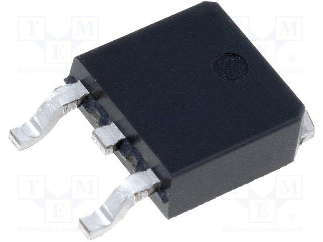
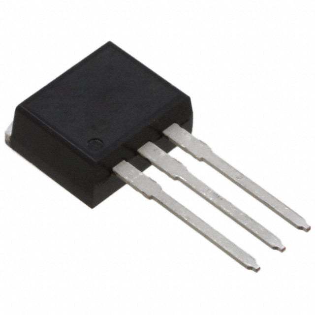
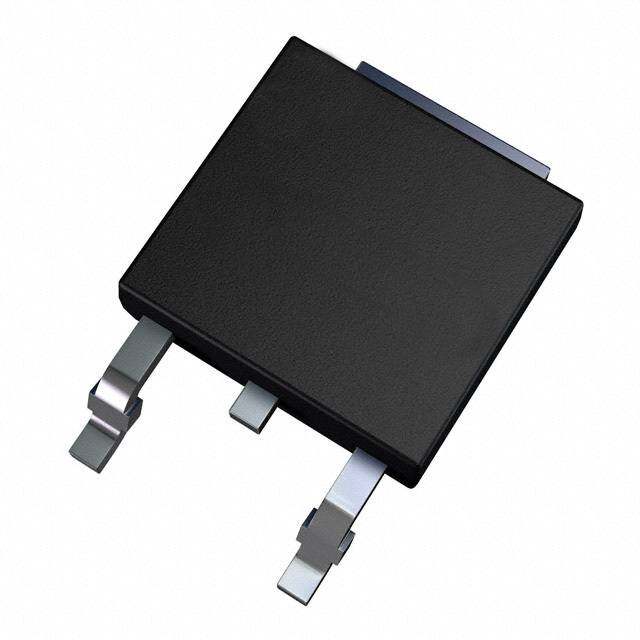
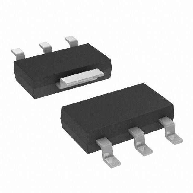
| 供应商器件封装 | TO-252,(D-Pak) |
| 其它名称 | 785-1103-2 |
| 其它图纸 |
|
| 功率-最大值 | 2.5W |
| 包装 | 带卷 (TR) |
| 安装类型 | 表面贴装 |
| 封装/外壳 | TO-252-3,DPak(2 引线+接片),SC-63 |
| 标准包装 | 2,500 |
| 漏源极电压(Vdss) | 60V |
| 电流-连续漏极(Id)(25°C时) | 26A(Tc) |


- 商务部:美国ITC正式对集成电路等产品启动337调查
- 曝三星4nm工艺存在良率问题 高通将骁龙8 Gen1或转产台积电
- 太阳诱电将投资9.5亿元在常州建新厂生产MLCC 预计2023年完工
- 英特尔发布欧洲新工厂建设计划 深化IDM 2.0 战略
- 台积电先进制程称霸业界 有大客户加持明年业绩稳了
- 达到5530亿美元!SIA预计今年全球半导体销售额将创下新高
- 英特尔拟将自动驾驶子公司Mobileye上市 估值或超500亿美元
- 三星加码芯片和SET,合并消费电子和移动部门,撤换高东真等 CEO
- 三星电子宣布重大人事变动 还合并消费电子和移动部门
- 海关总署:前11个月进口集成电路产品价值2.52万亿元 增长14.8%


PDF Datasheet 数据手册内容提取
AOD409/AOI409 60V P-Channel MOSFET General Description Product Summary • Trench Power MV MOSFET technology VDS -60V • Low RDS(ON) ID (at VGS=-10V) -26A • Low Gate Charge R (at V =-10V) < 40mΩ DS(ON) GS • Optimized for fast-switching applications R (at V =-4.5V) < 55mΩ DS(ON) GS Applications 100% UIS Tested 100% Rg Tested • Synchronus Rectification in DC/DC and AC/DC Converters • Industrial and Motor Drive applications TO252 TO-251A DPAK IPAK D TopView Bottom View Top View Bottom View D D G D S D G G D S S D G S S G Orderable Part Number Package Type Form Minimum Order Quantity AOD409 TO-252 Tape & Reel 2500 AOI409 TO-251A Tube 4000 Absolute Maximum Ratings T =25°C unless otherwise noted A Parameter Symbol Maximum Units Drain-Source Voltage V -60 V DS Gate-Source Voltage V ±20 V GS Continuous Drain TC=25°C I -26 Current TC=100°C D -18 A Pulsed Drain Current C I -80 DM Avalanche Current C I -26 A AS Avalanche energy L=0.1mH C E 34 mJ AS TC=25°C P 60 W Power Dissipation B TC=100°C D 30 TA=25°C P 2.5 W Power Dissipation A TA=70°C DSM 1.6 Junction and Storage Temperature Range T, T -55 to 175 °C J STG Thermal Characteristics Parameter Symbol Typ Max Units Maximum Junction-to-Ambient A t ≤ 10s 16.7 25 °C/W R Maximum Junction-to-Ambient A D Steady-State qJA 40 50 °C/W Maximum Junction-to-Case Steady-State RqJC 1.9 2.5 °C/W Rev.7.0: March 2018 www.aosmd.com Page 1 of 6
AOD409/AOI409 Electrical Characteristics (T =25°C unless otherwise noted) J Symbol Parameter Conditions Min Typ Max Units STATIC PARAMETERS BV Drain-Source Breakdown Voltage I =-250μA, VGS=0V -60 V DSS D V =-48V, V =0V -1 I Zero Gate Voltage Drain Current DS GS μA DSS T=55°C -5 J I Gate-Body leakage current V =0V, V =±20V ±100 nA GSS DS GS V Gate Threshold Voltage V =V I =-250mA -1.2 -1.9 -2.4 V GS(th) DS GS, D I On state drain current V =-10V, V =-5V -80 A D(ON) GS DS V =-10V, I =-20A 32 40 GS D mΩ R Static Drain-Source On-Resistance T=125°C 53 DS(ON) J V =-4.5V, I =-20A 43 55 mΩ GS D g Forward Transconductance V =-5V, I =-20A 32 S FS DS D V Diode Forward Voltage I =-1A,V =0V -0.73 -1 V SD S GS I Maximum Body-Diode Continuous Current -30 A S DYNAMIC PARAMETERS C Input Capacitance 2977 3600 pF iss C Output Capacitance V =0V, V =-30V, f=1MHz 241 pF oss GS DS C Reverse Transfer Capacitance 153 pF rss R Gate resistance f=1MHz 2 2.4 Ω g SWITCHING PARAMETERS Qg(10V) Total Gate Charge 44 54 nC Qg(4.5V) Total Gate Charge V =-10V, V =-30V, I =-20A 22.2 28 nC GS DS D Q Gate Source Charge 9 nC gs Q Gate Drain Charge 10 nC gd t Turn-On DelayTime 12 ns D(on) t Turn-On Rise Time V =-10V, V =-30V, R =1.5W, 14.5 ns r GS DS L tD(off) Turn-Off DelayTime RGEN=3W 38 ns t Turn-Off Fall Time 15 ns f trr Body Diode Reverse Recovery Time IF=-20A, dI/dt=100A/ms 40 50 ns Qrr Body Diode Reverse Recovery Charge IF=-20A, dI/dt=100A/ms 59 nC A. The value of R is measured with the device mounted on 1in2 FR-4 board with 2oz. Copper, in a still air environment with T =25°C. The Power qJA A dissipation P is based on R t≤ 10s and the maximum allowed junction temperature of 150°C. The value in any given application depends on DSM qJA the user's specific board design, and the maximum temperature of 175°C may be used if the PCB allows it. B. The power dissipation P is based on T =175°C, using junction-to-case thermal resistance, and is more useful in setting the upper dissipation D J(MAX) limit for cases where additional heatsinking is used. C. Single pulse width limited by junction temperature T =175°C. J(MAX) D. The R is the sum of the thermal impedance from junction to case R and case to ambient. qJA qJC E. The static characteristics in Figures 1 to 6 are obtained using <300ms pulses, duty cycle 0.5% max. F. These curves are based on the junction-to-case thermal impedance which is measured with the device mounted to a large heatsink, assuming a maximum junction temperature of T =175°C. The SOA curve provides a single pulse rating. J(MAX) G. The maximum current rating is package limited. H. These tests are performed with the device mounted on 1 in2 FR-4 board with 2oz. Copper, in a still air environment with T=25°C. A THIS PRODUCT HAS BEEN DESIGNED AND QUALIFIED FOR THE CONSUMER MARKET. APPLICATIONS OR USES AS CRITICAL COMPONENTS IN LIFE SUPPORT DEVICES OR SYSTEMS ARE NOT AUTHORIZED. AOS DOES NOT ASSUME ANY LIABILITY ARISING OUT OF SUCH APPLICATIONS OR USES OF ITS PRODUCTS. AOS RESERVES THE RIGHT TO IMPROVE PRODUCT DESIGN, FUNCTIONS AND RELIABILITY WITHOUT NOTICE. Rev.7.0: March 2018 www.aosmd.com Page 2 of 6
AOD409/AOI409 TYPICAL ELECTRICAL AND THERMAL CHARACTERISTICS 30 30 -10V -4.5V V =-5V -4V DS 25 25 -5V 20 20 -6V A) 15 A) 15 -I (D -3.5V -I(D 10 10 125°C 5 5 25°C V =-3V GS 0 0 0 1 2 3 4 5 1 2 3 4 5 -V (Volts) -V (Volts) DS GS Figure 1: On-Region Characteristics (Note E) Figure 2: Transfer Characteristics (Note E) 60 2 ) W 50 VGS=-4.5V sistance 11..68 VIDG=S-=2-01A0 V m 40 e R (ON) On- 1.4 RDS( 30 ed z VGS=-10V mali 1.2 VGS=-4.5V 20 Nor 1 ID=-20A 10 0.8 0 5 10 15 20 25 0 25 50 75 100 125 150 175 -I (A) Temperature (°C) D Figure 3: On-Resistance vs. Drain Current and Gate Figure 4: On-Resistance vs. Junction Temperature Voltage (Note E) (Note E) 80 1.0E+01 I =-20A D 1.0E+00 125°C m) W 60 A) 1.0E-01 (ON) -I (S 1.0E-02 125°C S( D R 40 1.0E-03 25°C 1.0E-04 25°C 20 1.0E-05 2 4 6 8 10 0.0 0.2 0.4 0.6 0.8 1.0 -VGS (Volts) -VSD (Volts) Figure 5: On-Resistance vs. Gate-Source Voltage Figure 6: Body-Diode Characteristics (Note E) (Note E) Rev.7.0: March 2018 www.aosmd.com Page 3 of 6
AOD409/AOI409 TYPICAL ELECTRICAL AND THERMAL CHARACTERISTICS 10 4500 V =-30V ID=S-20A 4000 D 8 3500 C F) 3000 iss olts) 6 ce (p 2500 V n (GS 4 cita 2000 V a - p 1500 a C 2 1000 C 500 oss C 0 0 rss 0 10 20 30 40 50 60 0 5 10 15 20 25 30 Q (nC) -V (Volts) g DS Figure 7: Gate-Charge Characteristics Figure 8: Capacitance Characteristics 1000.0 500 T =175°C J(Max) T =25°C 100.0 10ms 400 C 10ms mps) 10.0 RlimDSit(eOdN ) 110m0sm s er (W) 300 A w -I (D 1.0 DC 10ms Po 200 0.1 T =175°C 100 J(Max) T =25°C C 0.0 0 0.01 0.1 1 10 100 0.0001 0.001 0.01 0.1 1 10 100 -V (Volts) DS Pulse Width (s) V > or equal to 4.5V GS Figure 10: Single Pulse Power Rating Junction-to- Figure 9: Maximum Forward Biased Case (Note F) Safe Operating Area (Note F) 10 D=T /T In descending order nt TJ,PKo=nTC+PDM.ZqJC.RqJC D=0.5, 0.3, 0.1, 0.05, 0.02, 0.01, single pulse nsience RqJC=2.5°C/W Trasta 1 d si ee zR malimal Norher 0.1 Single Pulse PD CT ZJq Ton T 0.01 1E-05 0.0001 0.001 0.01 0.1 1 10 100 Pulse Width (s) Figure 11: Normalized Maximum Transient Thermal Impedance (Note F) Rev.7.0: March 2018 www.aosmd.com Page 4 of 6
AOD409/AOI409 TYPICAL ELECTRICAL AND THERMAL CHARACTERISTICS LI 30 tABVVD 80 DD Current 25 n (W) 60 anche 20 sipatio 40 val Dis eak A 15 ower 20 P P A), -I(D 10 T A=25°C 0 0.00001 0.0001 0.001 0 25 50 75 100 125 150 175 Time in avalanche, tA (s) TCASE (°C) Figure 12: Single Pulse Avalanche capability Figure 13: Power De-rating (Note F) 30 60 T =25°C A 25 50 A) 20 40 ng -I(D 15 er (W) 30 nt rati 10 Pow 20 e urr C 5 10 0 0 0 25 50 75 100 125 150 175 0.001 0.01 0.1 1 10 100 1000 Pulse Width (s) T (°C) CASE Figure 15: Single Pulse Power Rating Junction-to- Figure 14: Current De-rating (Note F) Ambient (Note H) Transient stance 101 RDTJq=,JPTAK=o=n5T/T0A° +PCD/MW.Z qJA.RqJA IDn= d0e.5s,c e0n.3d,i n0g.1 o, r0d.e0r5 , 0.02, 0.01, single pulse d si ee zR malimal 0.1 Norher PD Z JAqT 0.01 Single Pulse T on T 0.001 0.0001 0.001 0.01 0.1 1 10 100 1000 Pulse Width (s) Figure 16: Normalized Maximum Transient Thermal Impedance (Note H) Rev.7.0: March 2018 www.aosmd.com Page 5 of 6
AOD409/AOI409 Gate Charge Test Circuit & Waveform Vgs Qg + 10V + VDC Qgs Qgd - Vds VDC - DUT Vgs Ig Charge Resistive Switching Test Circuit & Waveforms RL Vds Vds 90% + Vgs DUT Vdd VDC Rg - 10% Vgs Vgs td(on) tr td(off) tf ton toff Unclamped Inductive Switching (UIS) Test Circuit & Waveforms L 2 Vds EA R = 1/2 LIAR BVDSS Id Vds + Vgs Vgs VDC Vdd IAR Rg - Id DUT Vgs Vgs Diode Recovery Test Circuit & Waveforms Vds + Q r r = - Idt DUT Vgs Vds - L Isd I trr Isd F dI/dt + I Vgs VDC Vdd RM Vdd - Vds Ig Rev.7.0: March 2018 www.aosmd.com Page 6 of 6