ICGOO在线商城 > 传感器,变送器 > 光学传感器 - 环境光,IR,UV 传感器 > AMS104Y
- 型号: AMS104Y
- 制造商: Panasonic Corporation
- 库位|库存: xxxx|xxxx
- 要求:
| 数量阶梯 | 香港交货 | 国内含税 |
| +xxxx | $xxxx | ¥xxxx |
查看当月历史价格
查看今年历史价格
AMS104Y产品简介:
ICGOO电子元器件商城为您提供AMS104Y由Panasonic Corporation设计生产,在icgoo商城现货销售,并且可以通过原厂、代理商等渠道进行代购。 AMS104Y价格参考。Panasonic CorporationAMS104Y封装/规格:光学传感器 - 环境光,IR,UV 传感器, Optical Sensor Ambient 580nm Current 4-SOIC (0.087", 2.20mm Width)。您可以下载AMS104Y参考资料、Datasheet数据手册功能说明书,资料中有AMS104Y 详细功能的应用电路图电压和使用方法及教程。
| 参数 | 数值 |
| 产品目录 | |
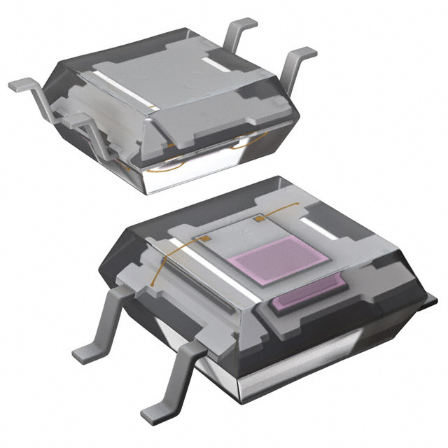
| 描述 | SENSOR LIGHT NAPICA 5V SMT 4SOP |
| 产品分类 | |
| 品牌 | Panasonic Electronic Components |
| 数据手册 | |
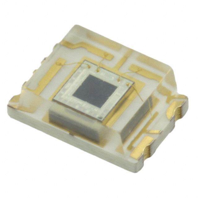
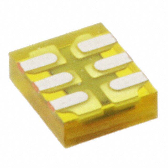
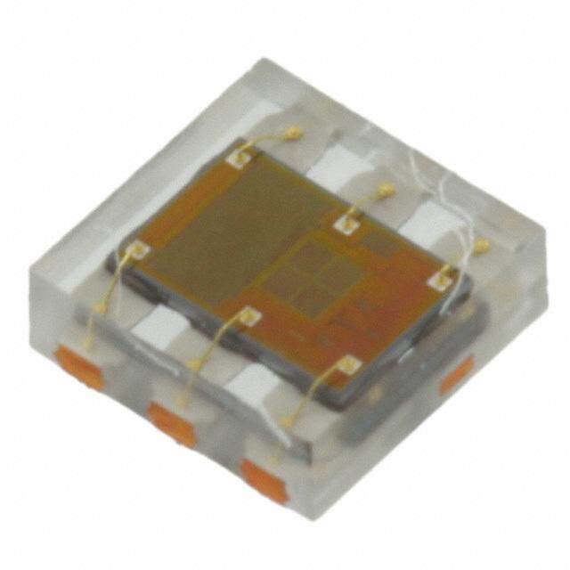
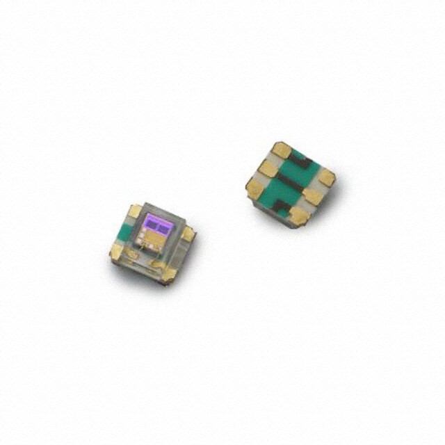
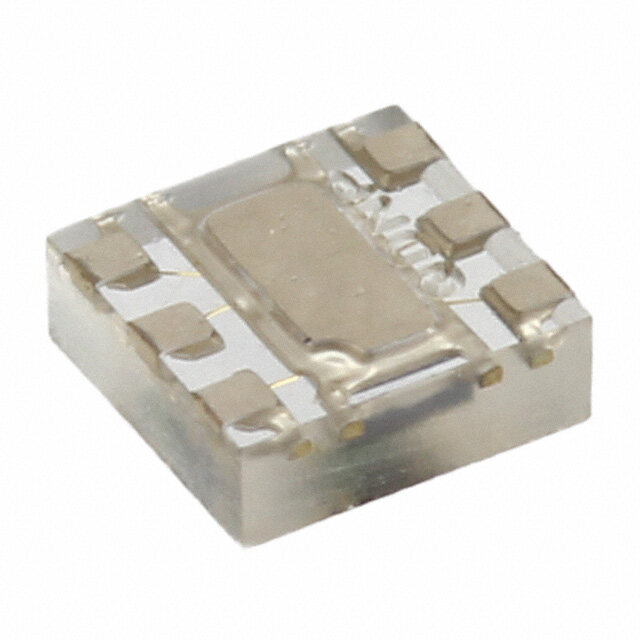
| 产品图片 |
|
| 产品型号 | AMS104Y |
| PCN过时产品 | |
| rohs | 无铅 / 符合限制有害物质指令(RoHS)规范要求 |
| 产品系列 | - |
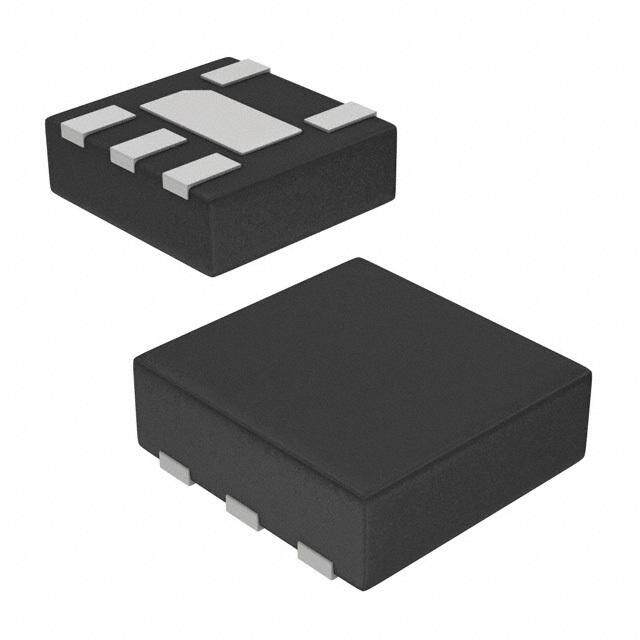
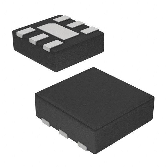
| 产品目录绘图 |
|
| 产品目录页面 | |
| 供应商器件封装 | 4-SMD |
| 其它名称 | 255-1848-1 |
| 其它有关文件 | |
| 包装 | Digi-Reel® |
| 安装类型 | 表面贴装 |
| 封装/外壳 | 4-SOIC(0.087",2.20mm 宽) |
| 工作温度 | -30°C ~ 85°C |
| 带接近传感器 | 无 |
| 标准包装 | 1 |
| 波长 | 580nm |
| 电压-电源 | 1.5 V ~ 6 V |
| 类型 | 环境 |
| 输出类型 | 电流 |



- 商务部:美国ITC正式对集成电路等产品启动337调查
- 曝三星4nm工艺存在良率问题 高通将骁龙8 Gen1或转产台积电
- 太阳诱电将投资9.5亿元在常州建新厂生产MLCC 预计2023年完工
- 英特尔发布欧洲新工厂建设计划 深化IDM 2.0 战略
- 台积电先进制程称霸业界 有大客户加持明年业绩稳了
- 达到5530亿美元!SIA预计今年全球半导体销售额将创下新高
- 英特尔拟将自动驾驶子公司Mobileye上市 估值或超500亿美元
- 三星加码芯片和SET,合并消费电子和移动部门,撤换高东真等 CEO
- 三星电子宣布重大人事变动 还合并消费电子和移动部门
- 海关总署:前11个月进口集成电路产品价值2.52万亿元 增长14.8%

PDF Datasheet 数据手册内容提取
Light Sensor (AMS1, 3, 4) Photo IC type high sensitive light sensor SENSOR FEATURES TYPICAL APPLICATIONS 1. Built-in optical filter for spectral SMD and Through-hole types response similar to that of the human eye. 1. Brightness detection for LCD 2. Photocurrent is proportional to backlight control for LCD devices illumination. (linear output) (LCD TVs, car navigation systems, and SMD type Through-hole type 3. Uses environmentally friendly mobile PCs). s silicon chips. 2. Brightness detection for circuits in sor residential lighting, lighting for en s security, and automatic lighting for ht g bicycle. Li 3. Household applicances (day/night energy savings for air conditioners Chip type and electric hot water pots, etc.) (2.0 × 1.25 × 0.55 mm) 4. Brightness detection for wall clocks (.079 × .049 × .022 inch) (radio clocks). Chip type 1. Brightness detection for LCD RoHS compliant backlight control for compact mobile devices (mobile phones and PDAs). 2. Brightness detection for controlling the keypad backlight in mobile phones. TYPES Part No. Type (shape) Photo current Tape and reel package Baggage package SMD type AMS104Y — 260 µA* Through-hole type AMS302T AMS302 Chip type 20 µA* AMS402Y — Standard packing: Tape and reel package SMD type: Carton: 3,000 pcs.; Case: 3,000 pcs. Tape and reel package Through-hole type: Carton: 2,000 pcs.; Case: 2,000 pcs. Baggage package Through-hole type: Carton: 500 pcs.; Case: 1,000 pcs. Tape and reel package Chip type: Carton: 3,000 pcs.; Case: 3,000 pcs. Notes:*Ev = 100 lx (Ev: Brightness, Fluorescent lamp is used as light source) Tape and reel package is standard packaging style for SMD and chip types. (“Y” and “T” at end of part number indicate packaging type.) RATINGS 1. Absolute maximum ratings (Measuring condition: ambient temperature: 25°C 77°F) Item Symbol AMS104/AMS302 AMS402 Remarks Reverse voltage VR –0.5 to 8 V –0.5 to 6 V — Photocurrent IL 5 mA 1 mA — Power dissipation P 40 mW 6 mW — Operating temperature Topr –30 to +85°C –22 to +185°F –30 to +85°C –22 to +185°F Non-condensing at low temperatures Storage temperature Tstg –40 to +100°C –40 to +176°F –40 to +100°C –40 to +176°F Non-condensing at low temperatures 2. Recommended operating condition Item Symbol AMS104/AMS302 AMS402 Remarks Minimum 1.5 V 1.5 V Reverse voltage VR — Maximum 6 V 5.5 V ASCTB242E 201209-T Panasonic Corporation Automation Controls Business Unit industrial.panasonic.com/ac/e
Light Sensor (AMS1, 3, 4) 3. Electrical and optical characteristics (Measuring condition: ambient temperature: 25°C 77°F) Item Symbol AMS104/AMS302 AMS402 Condition Peak sensitivity wavelength — λp 580 nm 560 nm — Minimum 9.1 µA 0.7 µA Photocurrent 1 TMyapxicimalum IL1 1163.9 µ µAA 11.3 µ µAA AAMMSS140042/: AVMR S= 330 V2,: VERV == 55 Vlx,* E1V = 5 lx*1 Minimum 182 µA 14 µA Photocurrent 2 TMyapxicimalum IL2 236308 µµAA 2206 µµAA AAMMSS140042/: AVMR S= 330 V2,: VERV == 150 V0, ElxV* 1= 100 lx*1 Photocurrent 3 Typical IL3 500 µA 35 µA AAMMSS140042/: AVMR S= 330 V2,: VERV == 150 V0, ElxV* 2= 100 lx*2 Dark current Maximum ID 0.3 µA 0.05 µA AAMMSS140042/: AVMR S= 330 V2,: VERV == 05 Vlx, EV = 0 lx s Switching time FRaislle t itmimee TTyyppiiccaall ttrf 88..55 mmss 11..22 mmss AAMMSS110044//AAMMSS330022:: VVCCCC == 53..00 VV,, VVOO == 21..55 VV,, RRLL == 55 kkΩΩ or s Notes:*1.Fluorescent lamp is used as light source. Ev = Brightness n e *2.CIE standard illuminant ‘A’ is used as light source. s ht *3.Measuring method for switching time. g Li Cathode IF White LED AMS∗∗∗ VR VCC AAMMSS140042/: A1M.5SV302: 2.5V 90% IF Anode VO 10% RL VO tr tf REFERENCE DATA 1. Power dissipation vs. ambient temperature 2. Relative sensitivity vs. wavelength 3. Dark current vs. ambient temperature characteristics characteristics characteristics Reverse voltage: 3V (AMS402), 5V (AMS104, Reverse voltage: 3V (AMS402), 5V (AMS104, AMS302) AMS302) Ambient temperature: 25°C 77°F 50 1.0 10 AMS402 AMS402 45 AMS104·AMS302 0.9 AMS104·AMS302 W wer dissipation, m 2233405050 Relative sensitivity 00000.....46857 Human spectral µDark current, A 0.00.111 o P 15 0.3 10 0.2 0.001 AMS402 AMS104·AMS302 5 0.1 0 0 0.0001 0 20 40 60 80 100 300 400 500 600 700 800 900 1000 1100 20 40 60 80 100 Ambient temperature, °C Wavelength, nm Ambient temperature, °C 4. Photocurrent vs. brightness characteristics 5. Relative photocurrent vs. ambient 6. Relative photocurrent vs. reverse voltage Light source: Fluorescent lamp temperature characteristics characteristics Reverse voltage: 3V (AMS402), 5V (AMS104, Light source: Fluorescent lamp, Brightness: 100 lx Light source: Fluorescent lamp, Brightness: 100 lx AMS302) Reverse voltage: 3V (AMS402), 5V (AMS104, Ambient temperature: 25°C 77°F Ambient temperature: 25°C 77°F AMS302) 10000 1.4 1.2 µPhotocurrent, A110100000 Relative photocurrent 11..02 Relative photocurrent 0001....4680 AMS402 0.8 1 AMS402 AMS104·AMS302 AMS402 0.2 AMS104·AMS302 AMS104·AMS302 0.1 0.6 0 1 10 100 1000 10000 -40 -20 0 20 40 60 80 100 0 1 2 3 4 5 6 7 8 Brightness, lx Ambient temperature, °C Reverse voltage, V ASCTB242E 201209-T Panasonic Corporation Automation Controls Business Unit industrial.panasonic.com/ac/e
Light Sensor (AMS1, 3, 4) 7. Switching time vs. resistive load characteristics Light source: White LED Power voltage: 3V (AMS402), 5V (AMS104, AMS302) Resistive load voltage: 1.5V (AMS402), 2.5V (AMS104, AMS302) Ambient temperature: 25°C 77°F 100 ms me, 10 g ti n hi witc S 1 s AMS402 tr sor AMS402 tf n AMS104·AMS302 tr se 0.1 AMS104·AMS302 tf ht 0.1 1 10 100 1000 Lig Resistive load, kΩ DIMENSIONS (mm inch) The CAD data of the products with a CAD Data mark can be downloaded from: http://industrial.panasonic.com/ac/e 1. SMD type (0.2) (.008) Recommended mounting pad CAD Data 4 3 (Top view) 0.25 .010 (0.1) (.004) .028.27 .132.26 .003.81.121.80 1 4 0.25 .010 Amplifier 1 .027.09 2 .00.264 2 3 1 Anode: – .10.5207 2 Anode: – 12 Anode 1.0 .039 3 Cathode: + 34 Cathode 4 Cathode: + .001.23 0.3 .00.0025 DETECTION AREA .012 Terminal thickness: t=0.125 1.27 .050 General Tolerance: ±0.1 ±.004 2. Through-hole type (0.17) CAD Data (.007) 1 Anode: – 2 Cathode: + DETECTION AREA 5.0±0.2 dia. .197±.008 dia. 5.8 dia. (1.0) .228 dia. (.039) 4.3±0.2 .169±.008 Max. 1.5 Max. .059 9.1 .358 1.0 .039 (1.0) (.039) 1 Amplifier 2 Max. 1.0 Max. .039 34±3 1.339±.118 1 Anode 2 Cathode 1 2 (2.5) (.098) 2-(cid:1)0.5 2-(cid:1).020 ((2.1.5040)) General Tolerance: ±0.5 ±.020 ASCTB242E 201209-T Panasonic Corporation Automation Controls Business Unit industrial.panasonic.com/ac/e
Light Sensor (AMS1, 3, 4) 3. Chip type (0.30) CAD Data 1(.012) (0.23) Recommended mounting pad (.009) 2 (Top view) 1 Anode 1.25 .049 2 Cathode (0.6) (0.6) DETECTION AREA (.024) (.024) (0.58) 1.45 (.023) .057 (1.2) 2.0 (.047) .079 0.55 (2.4) .022 (.094) Mark for indicating orientation (0.17) 1 Amplifier 2 (.007) 1 Anode (–) 2 Cathode (+) ors .10.427 General Tolerance: ±0.1 ±.004 s n e s ht g SAFETY PRECAUTIONS Li Be sure to obey the following in order to •Connect terminals correctly by verifying •For an impotant and serious application prevent injuries and accidents. the pin layout with the specifications in terms of safety, add protection circuit •Do not use the sensors under diagram or other instructions. or any other protection method. conditions that exceed the range of its Erroneous connections may lead to specifications. It may cause unexpected operating errors, overheating, smoke, or fire. overheating, smoke, or fire. CAUTIONS FOR USE 1. Applying stress that exceeds the 4) Devices and equipment used in 3) Storage under extreme conditions will absolute maximum rating assembly should also be grounded. cause soldering degradation, external If the voltage or current value for any of 5) When packing printed circuit boards appearance defects, and deterioration of the terminals exceeds the absolute and equipment, avoid using high-polymer the characteristics. The following storage maximum rating, internal elements will materials such as foam styrene, plastic, conditions are recommended: deteriorate because of the excessive and other materials which carry an •Temperature: 0 to 30°C 32 to 86°F voltage or current. In extreme cases, electrostatic charge. •Humidity: Less than 60% R.H. wiring may melt, or silicon P/N junctions 6) When storing or transporting sensor, (Avoid freezing and condensing) may be destroyed. the environment should not be generated •Atomosphere: No harmful gasses such Therefore the design should ensure that static electricity (for instance, the as sulfurous acid gas, minimal dust. the absolute maximum ratings will never humidity should be between 45 and *When mounting with solder, if thermal be exceeded, even momentarily. 60%), and sensor should be protected stress is applied to sensors that have 2. Deterioration and destruction using conductive packing materials. absorbed moisture, the moisture will caused by discharge of static 3. Just after supplying voltage, please vaporize, swelling will occur, and the electricity note that current in the sensor will be inside of the package will become This phenomenon is generally called not constant until internal circuit stressed. This may cause the package static electricity destruction. Static stability. surface to blister or crack. Therefore, electricity generated by various factors 4. Storage please take caution and observe the flows through the terminal and occurs to The sensors are transparent plastic soldering conditions in the following destroy internal elements. To prevent packages. They are sensitive to moisture section. problems from static electricity, the and come in moisture-proof packages. following precautions and measures Observe the following cautions when should be taken when using your device. storing. 1) Person handling sensor should wear 1) After the moisture-proof package is anti-static clothing and should be unsealed, take the sensors out of storage grounded through protective resistance as soon as possible (within 1 week of 500 kΩ to 1 MΩ. 30°C 86°F/60% R.H.). 2) A conductive metal sheet should be 2) If the devices are to be left in storage placed over the work table. Measuring for a considerable period after the instruments and jigs should be grounded. moisture-proof package has been 3) When using soldering irons, either use unsealed, it is recommended to keep irons with low leakage current, or ground them in another moisture-proof bag the tip of the soldering iron. (Use of low- containing silica gel (within 3 months at voltage soldering irons is also the most). recommended.) ASCTB242E 201209-T Panasonic Corporation Automation Controls Business Unit industrial.panasonic.com/ac/e
Light Sensor (AMS1, 3, 4) 5. Recommended soldering 2) The soldered position on leads should 8. Transportation conditions not be closer than 3mm .118inch to the Extreme vibration during transport will <SMD/Chip type> molding resin of this sensor. warp the lead or damage the sensor. 1) Recommended condition 6. Notes for mounting Handle the outer and inner boxes with (1) IR (Infrared reflow) soldering method 1) Temperature rise in the lead portion is care. highly dependent on package size. 9. Avoid using the sensor in T3 If multiple different packages are environments containing excessive T2 mounted on the same board, please amounts of steam, dust, corrosive T1 check your board beforehand in an actual gas, or where organic solvents are product, ensuring that the temperature of present. the solder area of the sensor terminals 10. Lead forming and cutting of t1 t2 falls within the temperature conditions of through-hole type item 5. 1) Lead forming must be done at normal T1 = 150 to 180°C 302 to 356°F 2) If the mounting conditions exceed the temperature before soldering TT23 == 223500°°CC 444862°°FF or less recommended solder conditions in item 2) The bent and cut position on leads nsors 5, resin strength will fall and the should not be closer than 3mm .118inch e t1 = 60 to 120 s or less mismatching of the heat expansion to the base of leads. ht s t2 = 30 s or less coefficient of each constituent material 3) Lead forming and cutting must be Lig (2) Soldering iron method will increase markedly, possibly causing done while fixing the base of leads. Tip temperature: 350 to 400°C 662 to cracks in the package, disconnections of 4) Avoid mounting with stress at the base 752°F bonding wires, and the like. For this of leads. Wattage: 30 to 60 W reason, please inquire with us about Soldering time: within 3 s whether this use is possible. *We don’t recommend soldering iron 7. Cleaning solvents compatibility method for chip type. We recommend dip cleaning with an 2) Do not do flow soldering. organic solvent for removal of solder flux <Through-hole type> etc. If you cannot avoid using ultrasonic 1) Recommended condition cleansing, please ensure that the (1) Double wave soldering method following conditions are met, and check T2 beforehand for defects. •Frequency: 27 to 29 kHz •Ultrasonic power: No greater than T1 0.25W/cm2 •Cleaning time: No longer than 30 s •Cleanser used: Asahiklin AK-225 t1 t2 t3 •Other: T1 = 120°C 248°F Submerge in solvent in order to prevent T2 = 260°C 500°F or less the PCB and sensors from being t1 = 120 s or less contacted directly by the ultrasonic t2+t3= 6 s or less vibrations. (2) Soldering iron method Note:Applies to unit area ultrasonic power for Tip temperature: 350 to 400°C 662 to ultrasonic baths. 752°F Wattage: 30 to 60 W Soldering time: within 3 s 11. The following shows the packaging format 1) SMD type tape and reel (mm inch) Type Tape dimensions Dimensions of tape reel 21.0±0.8 dia. 11.4±1.0 .827±.031 dia. .449±.039 Anode side Dpiicrekicntgion of 1.0.559+−00+−.1.00 d04i ad.ia. Device .000.28±±0.0.0052 mono utanpteed .1547.0±.±000.14 2.0.079±0±.1.004 1.0.7659±±0.0.104 .0729.0±.±002.50 7.107088±±2.0 7d9 iad.ia. Light sensor 8.0±0.2 NaPiCa .315±.008 60±0.5 dia. SMD type 2.362±.020 dia. AMS104Y .0519.5±.±001.32 .1342.62.4±±0.±0.100.41 .1547.0±.±000.14 1.0.039±0±.1.0 0d4i ad.ia. 3.1.53±80±.1.004 .094±.004 Cathode side 13.0±0.5 dia. Note) When picked from 1 and 4-pin side .512±.020 dia. (Please inquire for tape and reel packaging with 2-pin and 3-pin on the 9.0±0.3 pull-out side.) .354±.012 ASCTB242E 201209-T Panasonic Corporation Automation Controls Business Unit industrial.panasonic.com/ac/e
Light Sensor (AMS1, 3, 4) 2) Through-hole type tape and reel (mm inch) Type Tape dimensions Symbol Symbol Dimensions Remarks 12.7±0.3 Anode side Cathode side Feed hole pitch P0 .500±.012 P2 P ∆p ∆h Product interval pitch P .1520.07±±.10.309 6.35±1.3 Product distance P2 .250±.051 Product bottom 20.5±1.0 distance H .807±.039 H W2 Lead interval F .21.0504±±.00.250 s Light sensor L W1W0W Product slant ∆h 00±±.10.309 nsor NTharPoiuCgah -hole Product tilt ∆p 00±±.10.309 e ght s tAyMpeS302T P0 F D0 Tape width W .1780.90+−+−..001032..0590 Li Note: Zigzag tape style is used. 13.0±0.3 Holding tape width W0 .512±.012 Feed hole position W1 .93.504+−+−00....007532500 0 to 0.5 Holding tape distance W2 0 to .020 3.8±0.2 Feed hole diameter D0 .150±.008 0.5±0.2 Included holding Tape thickness t .020±.008 tape thickness Defective product L Max.: 11.0 .433 cutoff position 3) Chip type tape and reel (mm inch) Type Tape dimensions Dimensions of tape reel 21.0±0.8 dia. 11.4±1.0 .827±.031 dia. .449±.039 Direction of picking 1.0.559+−00+−.1.00 d04i ad.ia. An.o00d0.e82 ±±s0.0i.00d52e Dmoneo vutaincpetee d .1547.0±.±000.14 2.0.079±0±.1.004 1.0.7659±±0.0.104 .0729.0±.±002.50 7.107088±±2.0 7d9 iad.ia. Light sensor 8.0±0.2 NaPiCa .315±.008 60±0.5 dia. Chip type 2.362±.020 dia. AMS402Y 0.9±0.3 .20.8295±±.00.014 3.1.538±0±.1.004 .035±.012 4.0±0.1 0.8±0.1 dia. Cathode side 1.5±0.1 .157±.004 .031±.004 dia. .059±.004 13.0±0.5 dia. .512±.020 dia. 9.0±0.3 .354±.012 Light Sensor NaPiCa terminology Term Symbol Explanation Reverse voltage VR The applied voltage between the cathode and anode. Photocurrent IL The current that flows between the cathode and anode when light is applied. Power dissipation P The electric power loss that occurs between the cathode and anode. The workable ambient temperature range at which normal operation is possible under the condition of a Operating temperature Topr prescribed allowable loss. Storage temperature Tstg The ambient temperature range at which the sensor can be left or stored without applying voltage. Peak sensitivity wavelength λp The wavelength of light at which sensitivity is at its maximum. Dark current ID The current between the cathode and anode when reverse voltage is applied during darkness. Rise time tr Time required for the output waveform to rise from 10% to 90% when light is applied. Fall time tf Time required for the output waveform to fall from 90% to 10% when light is cut. ASCTB242E 201209-T Panasonic Corporation Automation Controls Business Unit industrial.panasonic.com/ac/e
 Datasheet下载


