 Datasheet下载
- 型号: AIC111RHB
- 制造商: Texas Instruments
- 库位|库存: xxxx|xxxx
- 要求:
| 数量阶梯 | 香港交货 | 国内含税 |
| +xxxx | $xxxx | ¥xxxx |
查看当月历史价格
查看今年历史价格
AIC111RHB产品简介:
ICGOO电子元器件商城为您提供AIC111RHB由Texas Instruments设计生产,在icgoo商城现货销售,并且可以通过原厂、代理商等渠道进行代购。 AIC111RHB价格参考¥54.16-¥90.33。Texas InstrumentsAIC111RHB封装/规格:接口 - 编解码器, Voice-Band Interface 16 b Serial 32-VQFN (5x5)。您可以下载AIC111RHB参考资料、Datasheet数据手册功能说明书,资料中有AIC111RHB 详细功能的应用电路图电压和使用方法及教程。
| 参数 | 数值 |
| ADC/DAC数 | 1 / 1 |
| ADC数量 | 1 |
| 产品目录 | 集成电路 (IC)半导体 |
| DAC数量 | 1 |
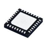
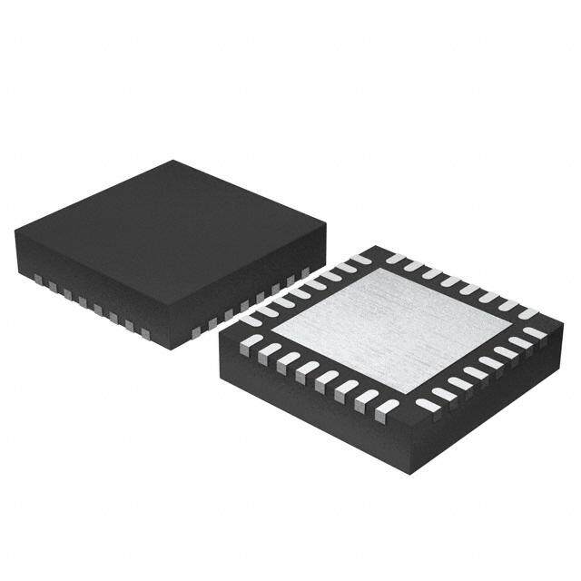
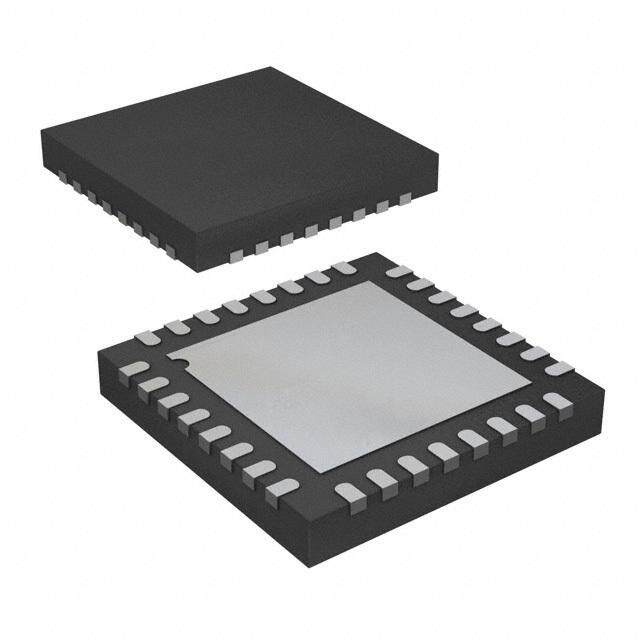
| 描述 | IC 1.3U DSP/UC AUDIO CODEC 32QFN接口—CODEC 1.3-V micro Power Single Ch Codec |
| 产品分类 | |
| 品牌 | Texas Instruments |
| 产品手册 | |
| 产品图片 |
|
| rohs | 符合RoHS无铅 / 符合限制有害物质指令(RoHS)规范要求 |
| 产品系列 | 接口 IC,接口—CODEC,Texas Instruments AIC111RHBmicroPOWER™ |
| 数据手册 | |
| 产品型号 | AIC111RHB |
| 三角积分 | 是 |
| 产品目录页面 | |
| 产品种类 | 接口—CODEC |
| 供应商器件封装 | 32-VQFN(5x5) |
| 信噪比 | 87 dB ADC |
| 信噪比,ADC/DAC(db)(典型值) | - |
| 其它名称 | 296-15335 |
| 分辨率 | 16 bit |
| 分辨率(位) | 16 b |
| 动态范围,ADC/DAC(db)(典型值) | - |
| 包装 | 管件 |
| 单位重量 | 72.200 mg |
| 商标 | Texas Instruments |
| 安装类型 | 表面贴装 |
| 安装风格 | SMD/SMT |
| 封装 | Tube |
| 封装/外壳 | 32-VFQFN 裸露焊盘 |
| 封装/箱体 | VQFN-32 |
| 工作温度 | 0°C ~ 70°C |
| 工作电源电压 | 1.1 V to 1.5 V |
| 工厂包装数量 | 73 |
| 接口类型 | Serial (SPI) |
| 数据接口 | 串行 |
| 最大工作温度 | + 70 C |
| 最小工作温度 | 0 C |
| 标准包装 | 73 |
| 电压-电源,数字 | 1.1 V ~ 1.5 V |
| 电压-电源,模拟 | 1.1 V ~ 1.5 V |
| 电源电压-最大 | 1.5 V |
| 电源电压-最小 | 1.1 V |
| 电源电流 | 350 uA |
| 类型 | 声带 |
| 系列 | AIC111 |
| 转换速率 | 40 kHz |
| 配用 | /product-detail/zh/AIC111EVM/296-18386-ND/809681 |


_renders/CS4265-CNZR.jpg)


- 商务部:美国ITC正式对集成电路等产品启动337调查
- 曝三星4nm工艺存在良率问题 高通将骁龙8 Gen1或转产台积电
- 太阳诱电将投资9.5亿元在常州建新厂生产MLCC 预计2023年完工
- 英特尔发布欧洲新工厂建设计划 深化IDM 2.0 战略
- 台积电先进制程称霸业界 有大客户加持明年业绩稳了
- 达到5530亿美元!SIA预计今年全球半导体销售额将创下新高
- 英特尔拟将自动驾驶子公司Mobileye上市 估值或超500亿美元
- 三星加码芯片和SET,合并消费电子和移动部门,撤换高东真等 CEO
- 三星电子宣布重大人事变动 还合并消费电子和移动部门
- 海关总署:前11个月进口集成电路产品价值2.52万亿元 增长14.8%


PDF Datasheet 数据手册内容提取
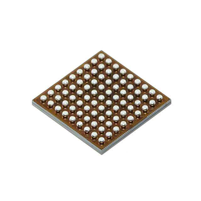
AIC111 www.ti.com SLAS382A–JUNE2003–REVISEDNOVEMBER2005 IC DESIGN SPECIFICATION 1.3-V microPower™ DSP/μC VOICE BAND AUDIO CODEC CheckforSamples:AIC111 FEATURES – -32-PinQFN5×5-mmPlasticPackage 1 • SingleChannelCodec – -32-PadBumpedDieinWafflePack(wafer 2 scalepackaging) • NoiseShapedDeltaSigmaADCandDAC Technology APPLICATIONS • LowSupplyVoltageandCurrent: • HearingInstruments – 1.3-VTypicalPowerSupply • PersonalMedicalDevices – 350-µATypicalSupplyCurrentDrain • HearingProtection • PowerSupplyUpMonitorandLowBattery MonitorThatAlsoAutomaticallyShutsOffH- • AuralProcessing BridgeOutputWhenBatteryDecaysBelow • Low-PowerHeadsets 1.05VinaNontransientManner DESCRIPTION • Typical2.4-µVrmsInputReferredNoiseWith 0.01%TotalHarmonicDistortionforFrontEnd The AIC111 IC design specification serves to provide and108-dBDynamicRange product development teams with a guideline for how the AIC111 IC is specified and programmable options • ADCHas87-dBDynamicRangeWith73-dB that are available. The document outlines a top-level TotalHarmonicDistortion100Hz-10kHz,40- block description of the IC along with system kHzSamplingRate specifications and functions. Individual block • Typical55-dBPSRR100Hzto10kHzfor descriptions and target specifications are also AnalogFrontEnd outlined. • LowNoiseProgrammableGain The Texas Instruments AIC111 is a TI µPower DSP Amplifier/CompressorFrontEndWith compatible, or microcontroller compatible audio ProgrammableFastandSlowAttackand codec product, or analog interface circuit. The DecayRatesWithDualorSingleAttackand AIC111 is part of a comprehensive family of DSP/µC DecayRateOption based high-performance analog interface solutions. The AIC111 is targeted primarily at personal medical • TypicalOutputNoiseof12µVrmsWith0.05% devices, such as hearing instruments, aural TotalHarmonicDistortionforDeltaSigmaDAC preprocessing applications, and low-power headset andH-BridgeOutputDriver applications. The AIC111 is used in any design • LowJitterOscillatorThatGeneratesall requiring a programmable time constant InternalClocksandGenerates5-MHzOutput PGA/compressor interface, high dynamic range DSP/µCClock analog-to-digital converter, an external DSP/µC handling signal processing, or a low distortion digital- • RegulatedBandgapVoltageReference to-analog converter with a balanced H-Bridge • ProgrammableFunctionalityviaDigitalSerial speaker driver. It supports a CMOS digital interface Interface tailored for TI DSPs with the McBSP protocol such as – McBSPInterface,DSPProtocol TMS320VC54x™ DSP family and SPI-based controllers such as TI MSP430x family of – TITMS320VC54x™,TMS320VC55x™DSPs microcontrollers. The AIC111 also has an external – SPIInterface,MicrocontrollerProtocol microphone or sensor supply and bias and power – TIMSP430xx supplyuplow-batterymonitorindicator. • ExternalChipPowerDownandReset • Availablein: 1 Pleasebeawarethatanimportantnoticeconcerningavailability,standardwarranty,anduseincriticalapplicationsof TexasInstrumentssemiconductorproductsanddisclaimerstheretoappearsattheendofthisdatasheet. microPowerisatrademarkofTexasInstruments. 2 UNLESS OTHERWISE NOTED this document contains Copyright©2003–2005,TexasInstrumentsIncorporated PRODUCTION DATA information current as of publication date. Products conform to specifications per the terms of Texas Instruments standard warranty. Production processing does not necessarilyincludetestingofallparameters.
AIC111 SLAS382A–JUNE2003–REVISEDNOVEMBER2005 www.ti.com Thesedeviceshavelimitedbuilt-inESDprotection.Theleadsshouldbeshortedtogetherorthedeviceplacedinconductivefoamduring storageorhandlingtopreventelectrostaticdamagetotheMOSgates. This integrated circuit can be damaged by ESD. Texas Instruments recommends that all integrated circuits be handled with appropriateprecautions.Failuretoobserveproperhandlingandinstallationprocedurescancausedamage. ESDdamagecanrangefromsubtleperformancedegradationtocompletedevicefailure.Precisionintegratedcircuitsmaybemore susceptibletodamagebecauseverysmallparametricchangescouldcausethedevicenottomeetitspublishedspecifications. The AIC111 comes in a 32-pin QFN 5×5-mm package. A 32-pad solder ball bumped flip chip die that comes in wafflepacksortapeandreelisinpreviewandwillbeavailable3rdquarter2003. AVAILABLEOPTIONS(1) PartNumber Package AIC111RHB 32-pinQFN(5mmx5mm),intube. AIC111RHBR 32-pinQFN(5mmx5mm),tapeandreel AIC111YE 32-padwafflescalechippackage,bumpeddieinwafflepack(commercial) AIC111YE 32-padwafflescalechippackage,bumpeddieinwafflepack(industrial) AIC111YER 32-pad(WSCP)bumpeddieintapeandreel (1) Forthemostcurrentpackageandorderinginformation,seethePackageOptionAddendumattheendofthisdocument,orseetheTI websiteatwww.ti.com. ABSOLUTE MAXIMUM RATINGS overoperatingfree-airtemperaturerangeunlessotherwisenoted((1))((2)) UNIT Inputvoltage AIorDIpins -0.3Vto4V Powersupply VDD,powerpins -0.3Vto4.5V Latch-uptolerance JEDEClatch-up(EIA/JEDS78) 100mA Commerical 0°Cto70°C T Operatingfree-airtemperaturerange, A Industrial −40°Cto85°C Functionaltemperaturerange -15°Cto85°C Reflowtemperaturerange(flipchip) 220°Cto230°C T Storagetemperaturerange -40°Cto125°C stg Storagehumidity 65%R.H. (1) Stressesbeyondthoselistedunderabsolutemaximumratingsmaycausepermanentdamagetothedevice.Thesearestressratings only,andfunctionaloperationofthedeviceattheseoranyotherconditionsbeyondthoseindicatedunderrecommendedoperating conditionsisnotimplied.Exposuretoabsolute-maximum-ratedconditionsforextendedperiodsmayaffectdevicereliability. (2) SpecificationsareassuredoperatingatmaximumdevicelimitsforQFNpackageonly,unlessotherwisespecified. ELECTRICAL CHARACTERISTICS INPUT/OUTPUT,OPERATINGTEMPERATUREAT25°C PARAMETER TESTCONDITION MIN TYP MAX UNIT Digitalinterface(see (1)and (2)) BUF_DVDD(seeNote (1)) 3.6 V BUF_DVDD- V High-levelinputvoltage V IH 0.2 BUF_DVSS+ V Low-levelinputvoltage V IL 0.2 V High-leveloutputvoltage BUF_DVDD V OH V Low-leveloutputvoltage BUF_DVSS V OL Maximumallowedinputvoltage(AVIN) Differential 450 mVpk (1) DVDD,VDD_OSC,andAVDDshouldbewithin50mV,preferablyconnectedtogether.AVSS1,2,DVSS,andVSS_OSCshouldbe within50mV,preferablyconnectedtogether. (2) Maximum(0.9V,DVDD-0.5V)≤BUF_DVDD≤3.6V 2 Copyright©2003–2005,TexasInstrumentsIncorporated
AIC111 www.ti.com SLAS382A–JUNE2003–REVISEDNOVEMBER2005 ELECTRICAL CHARACTERISTICS (continued) INPUT/OUTPUT,OPERATINGTEMPERATUREAT25°C PARAMETER TESTCONDITION MIN TYP MAX UNIT Inputimpedance(AVIN)(see (3)) Nominalgain=50x 20 kΩ Inputcapacitance(AVIN) 5 pF Microphonebiasvoltage(MIC_VSUP) 20-μAmaximum 0.87 0.94 0.99 V Microphonebiasresistor(MIC_BIAS) 27 29.1 31 kΩ DACfullscaleoutput FixedQ 3/4HB_VDD H-bridgeamplifieroutput V differential AdaptiveQ HB_VDD PP Outputresistance Differential,HB-V =1.3V 20or40 Ω DD (3) Drivingsingle-ended:Rin=R×[(1+A)/(2+A)],A=PGACGain(linear),R=20.4kΩforA≥4or20.4kΩ×(4/A)forA<4.Rin(min)=17kΩ (A=4),Rin(max)=59.89kΩ(A=0.89),Rin(nom)=20kΩ(A=50). Copyright©2003–2005,TexasInstrumentsIncorporated 3
AIC111 SLAS382A–JUNE2003–REVISEDNOVEMBER2005 www.ti.com TERMINAL ASSIGNMENTS N D W SS_REF FILTDD T_RST/P T/LBM SS2 LK V RV X S V C A VA E R D S 32 3130 2928 27 26 FRAME AVSS1 1 25 24 SDIN AVSS2 2 AVINP 3 AIC111 23 SDOUT AVINM 4 22 BUF_DVSS 21 BUF_DVDD VMID_FILT 5 Bumped Side 20 DVDD MIC_BIAS 6 19 DVSS1 VREF 7 18 MCLK MIC_VSUP 8 9 10 11 121314151617 IMODE Alignment Marker S C C P PDM M SUB_VS VDD_OS VSS_OS HB_VSS_ VOUT_HB_VDVOUT_ HB_VSS_ Bumped View (0,0) SUB_VSS VDD_OSC VSS_OSC HB_VSS_P VOUT_PHB_VDDVOUT_MHB_VSS_M loFcoartP ieoCxnBa sc Vet iebe uwSmpepc. Section 2.2 9 10 11 121314151617 IMODE MIC_VSUP 8 VREF 7 18 MCLK 19 DVSS1 MIC_BIAS 6 Back Side 20 DVDD VMID_FILT 5 21 BUF_DVDD AVINM 4 22 BUF_DVSS AVINP 3 AIC111 23 SDOUT AVSS2 2 24 SDIN AVSS1 1 25 32 3130 2928 27 26 FRAME A VA ER D S V RV XS V C S FD TT S L S_RE ILTD _RST/LBM S2 K F /P W D N Figure1. AIC111YEBumpedViewandPCBFlippedPinPlacements 4 Copyright©2003–2005,TexasInstrumentsIncorporated
AIC111 www.ti.com SLAS382A–JUNE2003–REVISEDNOVEMBER2005 F E M S_R LT D S LB S K ME S FI D S T/ S L A V R V V S V C R A V A D R D S F 32 31 30 29 28 27 26 25 AVSS1 1 24 SDIN AVSS2 2 23 SDOUT AVINP 3 22 BUF_DVSS AVINM 4 21 BUF_DVDD AIC111RHB VMID_FILT 5 20 DVDD MIC_BIAS 6 19 DVSS VREF_BG 7 18 MCLK MIC_VSUP 8 17 IMODE 9 10 11 12 13 14 15 16 S C C P P D M M SUB_VS VDD_OS VSS_OS HB_VSS_ VOUT_ HB_VD VOUT_ HB_VSS_ Figure2. AIC111RHB32-PinQFNPinout TerminalFunctions TERMINAL Type Description NO. Name 1 AVSS1 GND GroundreturnforADCanalogcircuits 2 AVSS2 GND GroundreturnforPGACandMICpoweranalogcircuits 3 AVINP AI Noninvertingdifferentialanaloginputcoupledthroughanexternal1-μFcapacitortoexternal microphoneoutput 4 AVINM AI Invertingdifferentialanalogsignalinputcoupledthroughanexternal1-μFcapacitortoground 5 VMID_FILT AO Midsupplyacgroundreferencefilterpinbypassedbya1-μFcapacitorconnectedtoground 6 MIC_BIAS AO Sourceconnectionofexternalmicrophonesourcefollowerpreamp.(Provides29.1kΩtoAVSS2) 7 VREF AO Bandgapreferenceoutputbypassedbyexternal1-μFVREFfiltercapacitor 8 MIC_VSUP AO Supplyvoltageforexternalmicrophonesourcefollowerpreampbypassedwithanexternal0.1-μF capacitor 9 SUB_VSS GND IsolatedsubstrateVSSforanalogcircuits 10 VDD_OSC VDD Powerpinforinternaloscillator 11 VSS_OSC GND Groundreturnforinternaloscillator 12 HB_VSS_P GND GroundreturnfornoninvertingstackofH-bridgeamplifier 13 VOUT_P AO NoninvertingH-bridgeoutputvoltage 14 HB_VDD VDD PowerpinforH-bridgeamplifier 15 VOUT_M AO InvertingH-bridgeoutputvoltage Copyright©2003–2005,TexasInstrumentsIncorporated 5
AIC111 SLAS382A–JUNE2003–REVISEDNOVEMBER2005 www.ti.com TerminalFunctions(continued) TERMINAL Type Description NO. Name 16 HB_VSS_M GND GroundreturnforinvertingstackofH-bridgeamplifier 17 IMODE DI Digitalinterfaceformatselectionpin 18 MCLK DO 5-MHzoutputclockforexternalDSP/μC 19 DVSS1 GND Groundreturnfordigitalcircuits 20 DVDD VDD Powerpinfordigitalcircuits 21 BUF_DVDD VDD PowerpinforinterfacedigitalI/Ocircuits 22 BUF_DVSS GND GroundreturnforinterfacedigitalI/Ocircuits 23 SDOUT DO Digitalinterfaceserialdataoutputpin 24 SDIN DI Digitalinterfaceserialdatainputpin 25 FRAME DO Digitalinterfaceserialdataframer 26 SCLK DO Digitalinterfaceserialshiftclock 27 DVSS2 GND Groundreturnfordigitalcircuits 28 RST/LBM DO Providesexternalresetandlowbatterymonitor 29 EXT_RST/PWDN DI Powersdownallanalogblocksandholdsdigitaloutputslowuntilinternalsystemisup 30 AVDD VDD VDDpowerpinforanalogcircuits 31 VRFILT AO PositiveADCreferencepinbypassedwith1-μFcapacitortoAVSS_REF 32 AVSS_REF GND GroundforADCvoltagereference Figure3. FUNCTIONALBLOCKDIAGRAM M MID_FILT UB_VSS VDD VSS_REF RFILT VSS B_VDD B_VSS_P HB_VSS_ V S A A V A H H AVINP Delta Dec. Delta H-Bridge VOUT_P RC Filter PGA/Compressor Flt Sigma & Sigma Speaker AVINM ADC HPF DAC Driver VOUT_M MIC_VSUP MIC/Sensor DVDD Biases Power and POR RST/LBM MIC_BIAS Bias Generator Digital DVSS Interface BUF_DVDD VDD_OSC Output Buffers Oscillator Bandgap VREF N BUF_DVSS VSS_OSC Reference D W P T/ S R E K E T N K EXT_ IMOD SCL FRAM SDOU SDI MCL OPERATION The power source may be a zinc-air battery operating at a typical voltage of 1.3 V. A single external de-coupling capacitorof1μFisrecommendedonthemainpowersupply. 6 Copyright©2003–2005,TexasInstrumentsIncorporated
AIC111 www.ti.com SLAS382A–JUNE2003–REVISEDNOVEMBER2005 VOLTAGEandCURRENT,OPERATINGTEMPERATUREAT25°C PARAMETER TESTCONDITION MIN TYP MAX UNIT AVDD,DVDD(AllpinsoftypeAVDD,DVDD Steady-statebatterysupply 1.1 1.3 1.5 V inpin-outtable) • Unloaded:H-Bridgeoutputopen • Microphone resistor model connected (see I (supplycurrent) Figure5) 350 μA S • Powersupplies=1.3V • Noreceiverattached FUNCTIONAL INPUT CHANNEL PERFORMANCE REQUIREMENTS The front end is defined as the differential signal path from the PGA/compressor inputs, AVINP, and AVINM throughthedelta-sigmaADCanddecimationfilter. TypicalConditions;deviationsarenotedintable. • OperatingTemperatureRange:0°Cto70°C.Allspecificationareat25°Cand1.3Vunlessotherwisenoted. • AVDD,DVDDrange:1.1Vto1.5V • AVINP,AVINMinputs:ACcoupled,Frequencyrangingfrom100Hz-10kHz • MeasurementBandwidth:100Hz-10kHzA-weighted. • Idlechanneldefinition:AVINPandAVINMarebothac-coupledtoAVSS. • TypicalPGACgainrangeis-1dBto40dB. • Maximuminputvoltage:450mVpk. PARAMETER TESTCONDITION MIN TYP MAX UNIT Broad-bandnoise Inputreferredidlechannel 2.4 μVRMS THD(lowlevel) AVIN≤PGACthreshold(seeNote (1)) 0.01 0.2% DCOffset Idlechannel -5 0 5 mV Droopat10kHz Referencedtoamplitudeat1kHz 1.2 dB (1) PGACthreshold=PGACthresholdvoltage/maximumgainofPGAC. 0 0 -10 -2 -20 -4 -30 -6 B B -8 d -40 d ain - -50 ain - -10 G G -60 -12 -70 -14 -80 -16 -18 -90 -100 -20 0 10 20 30 40 50 60 70 80 90 100 0 2 4 6 8 10 12 14 16 18 20 f - Frequency - kHz f - Frequency - kHz Figure4. InputChannelFrequencyResponseWithHPFBypassed Copyright©2003–2005,TexasInstrumentsIncorporated 7
AIC111 SLAS382A–JUNE2003–REVISEDNOVEMBER2005 www.ti.com ANALOG-TO-DIGITAL CONVERTER FILTERED INPUT VOLTAGE REFERENCE Function - Filters analog supply AVDD for DS-ADC reference. With a recommended 0.1-μF external capacitor between pins VRFILT and AVSS_REF, the pole is set at approximately 72 Hz, with 1 μF, the pole is set at approximately7Hz. PROGRAMMABLEGAINAMPLIFIERANDCOMPRESSOR Function: The programmable gain amplifier and compressor (PGAC) amplifies the microphone or sensor output signal, provides an appropriate impedance to the microphone buffer or sensor, and provides input gain compression limiting depending on the input signal level if one is not using the fixed gain mode, where the PGAC gain is set by selected register bits. Input compression limiting is discrete automatic gain correction (AGC) based on detecting the peak input signal level using a peak detector circuit that has programmable time responses to provide AGC control, and is intended to prevent a steady state input level up to the defined PGAC limit from being clipped. The attack/release times of the PGAC are programmable by internal clock selection inside the PGACdigitallevelcircuitrythataffectstherateofgainchanges. The PGAC has four modes of operation: automatic dual-rate (default), automatic single-rate, fixed single-rate, andfixedimmediate.Modeselectioniscontrolledbybits3and2ofthePDCREGregister. AUTOMATICDUAL-RATEMODE(00,DEFAULT): In this mode of operation, the PGAC has two attack (gain decrease) rates and two release (gain increase) rates, which may be selected by programming the FASTARREG and FORMAT4 registers. Internally, two counters are used to control the compressor gain. The fast rate counter responds at the fast attack and release rates, and it counts down at the attack rate to decrease the PGAC gain if the output of the PGAC is instantaneously larger thanapresetthreshold(PGAC_THRES=400-mVpeak),oritcountsuptoincreasethegain,uptothemaximum allowedgainassetbythePGACREGregister,iftheoutputofthePGACfallsbelowasecondthreshold,whichis 3 dB lower (283-mV peak), which provides hysteresis. Before the gain is allowed to increase, the signal at the output of the PGAC must be below the lower threshold for a period of time which is controlled by bit 4 of PDCREG, and can be 50 ms (0, default) or 25 ms (1). The slow-rate counter responds at the slow attack and release rates, and it attempts to track the state of the fast rate counter. The PGAC gain is determined by whichever counter is smaller. In this way, the PGAC can respond and recover rapidly to short signal bursts while respondingmoreslowlytothesignalaverage. AUTOMATICSINGLE-RATEMODE(01): In this mode of operation, the PGAC has one attack rate and one release rate, which may be selected by programming the FASTARREG register. The operation of the PGAC is similar to the dual-rate mode, except that theslow-ratecounterisdisabledandthePGACgainissolelydeterminedbythefast-ratecounter. FIXEDSINGLE-RATEMODE(10): In this mode of operation, the PGAC gain tracks the value specified in the PGACREG register regardless of the signal amplitude, and changes in PGACREG cause the gain to decrease or increase at the corresponding fast attackorreleaseratespecifiedintheFASTARREGregister. FIXEDIMMEDIATEMODE(11): In this mode of operation, the PGAC gain tracks the value specified in the PGACREG register regardless of the signal amplitude, and changes in PGACREG cause the gain to change immediately to the desired gain without steppingthroughtheintermediategainstates. Bit 7 of the PGACREG register controls the PGAC gain read mode. While this bit is low (default), reading PGACREG returns the contents of PGACREG. However, if this bit is set high, then any subsequent read(s) of PGACREG returns the actual, instantaneous PGAC gain. This information may be useful, for example, for dynamicrangeexpansion,effectivelyundoingthecompressioneffectintheautomaticmodesofoperation. CHARACTERISTICS :CompressionlimitsthePCAGoutput.PGACREGisaprogrammableregister. 8 Copyright©2003–2005,TexasInstrumentsIncorporated
AIC111 www.ti.com SLAS382A–JUNE2003–REVISEDNOVEMBER2005 SPECIFICATIONSAT25°C,AVDD=1.3V(2) (3) PARAMETER TESTCONDITIONS MIN TYP MAX UNIT InputSignalParameters Maximumsignalswing Gain=-1dB 900 mV PP BlockParameters Gainsizestep 0.3 0.5 0.7 dB (2) Basedonasystemclockof1.280MHz. (3) Forfixedgainmodetherateis80KdB/stonewprogrammedvalueofgain.Allintermediate0.5dBgainstepsarepassedthroughto reachnewgain. DELTA SIGMA A/D CONVERTER/ANTI-ALIAS FILTER Function:Converts the PGAC differential outputto a digital word with an equivalent dynamic range of approximately14bits. Characteristics: The delta sigma ADC has a 64 oversampling ratio, a 1.28-MHz master clock, and a 40-kHz output data rate. Digital coding is 2s complement. Tones are at least 12 dB below broadband noise level. Full- scalesignalrangecorrespondsto+215-1,-215 Table1.SPECIFICATIONSAT25°C,AVDD=1.3V PARAMETER TESTCONDITIONS MIN TYP MAX UNIT Blockparameters Dynamicrange -3dBrel.toreference 87 dB Inputsamplerate 1.28 MHz Outputsamplerate 40 kHz THD BW:100Hz-10kHz 85 dB DIGITAL HIGH-PASS FILTER Function:Provide a high-pass filter in ADC signal path. The high-pass filter (HPF first order) removes dc offsets introducedintothechannel.FORMAT1registerselectionsfora50Hz,100Hz,orbypassareavailable. Characteristics: Programmable selections for a 50 Hz, 100 Hz, or bypass are available. The default HPF pole is 50Hz. Table2.SPECIFICATIONS PARAMETER TESTCONDITIONS MIN TYP MAX UNIT HPFcornerfrequency -3dBnommode 50 Hz DELTA SIGMA DAC Function:Generates an over-sampled bit string to drive the H-bridge output amplifier such that when filtered reproducesthedesiredanalogwaveform. Characteristics:A32timesover-sampledmodulatormulti-bitdesign. Table3.SPECIFICATIONS PARAMETER TESTCONDITIONS MIN TYP MAX UNIT fd Signal;BW=10kHz 40 kHz (input_data) f 640 kHz clk Copyright©2003–2005,TexasInstrumentsIncorporated 9
AIC111 SLAS382A–JUNE2003–REVISEDNOVEMBER2005 www.ti.com H-BRIDGE OUTPUT DRIVER Function: An H-bridge output driver efficiently converts the delta sigma DAC modulator output signals. The externalloadprovidesthelow-passfilteringthatrecoversthedifferentialanalogsignalfromtheH-bridge. Characteristics: Standard H-bridge configuration with transistors sized to differentially drive the load impedance. Theloadimpedanceiscomplexandafunctionoffrequency. H-Bridge Load Switching Noninverting Phase Inverting Phase VDD (vbat) VDD (vbat) OUTPM OUTMM OUTPM OUTMM OUTP Receiver OUTM OUTP Receiver OUTM Load Load OUTMP OUTPP OUTMP OUTPP AVSS AVSS A. VDD does not necessarily have to be connected to the same potential as AVDD, it could be connected to a higher potentialthanAVDD,equaltoAVDD,butnotlessthanAVDD. Figure5. DefinitionofPhaseandOutputSwitchingCurrentPolarity Table4.SPECIFICATIONSAT25°C,HB_VDD=1.3V PARAMETER TESTCONDITIONS MIN TYP MAX UNIT BlockParameters DCoffset Idlechannel;DifferentialacrossVOUT_PandVOUT_M -5 0 5 mV Idlechannel,measuredatoutputofchannel, FixedQ 33 Broadbandnoise μVrms BW=100Hz-10kHz,HB_VDD=1.3V,A-weighted AdaptiveQ 12 THD BW=100Hz-10kHz 0.03% Switchingfrequency 640 kHz 3/4 FixedQ Maximumoutputswing HB_VDD V PP AdaptiveQ HB_VDD MICROPHONE POWER SUPPLY Function: The microphone power supply circuit provides a constant power supply voltage and bias current for the microphone preamp or sensor bias, provides a low-noise voltage reference (ac ground) for the PGAC, provides regulated PGAC comparator threshold levels, provides bandgap regulated POR comparator trip voltage levels,andprovidesabandgapregulatedcurrentforthebiasesgeneratorcircuit. Characteristics: The low-dropout regulator configuration or single stage, single-pole amplifier drives an external 0.1-μF capacitor. The regulator does not oscillate under no-load or loaded conditions. The circuit supplies up to 50-μAofcontinuouscurrent. Table5.SPECIFICATIONSAT25°C,AVDD=1.3V PARAMETER TESTCONDITIONS MIN TYP MAX UNIT MIC_VSUP I =20μA 0.87 0.94 0.97 V L VMID_FILT 0.59×AVDD 0.78 V PSRR 0.1-μFexternalbypasscapfromMIC_VSUPtoAVSS2. 55 dB 10 Copyright©2003–2005,TexasInstrumentsIncorporated
AIC111 www.ti.com SLAS382A–JUNE2003–REVISEDNOVEMBER2005 Table5.SPECIFICATIONSAT25°C,AVDD=1.3V(continued) PARAMETER TESTCONDITIONS MIN TYP MAX UNIT Outputimpedance 1.5 kΩ MCLK Output Function:Providesaclocksignalforexternaluse. Table6.SPECIFICATIONSAT25°C,VDD_OSC,DVDD,BUF_DVDD=1.3V PARAMETER TESTCONDITIONS MIN TYP MAX UNIT Frequency 4.7 5.12 5.5 MHz Jitter RMSjitter 150 ps Dutycycle 50% POWER-ON RESET Function:Provides a reset signal upon power up (stable voltage reference) that initializes the digital interface. It also provides a gating signal to the delta-sigma DAC modulator to prevent audible pops and clicks from erroneous data sent to the H-bridge circuit at power up and during periods when battery voltage has degraded below 1.05 V for an extended period of time (typically greater than 44 μs). The reset signal is asynchronous to MCLK.Digitalinterfacedoesnotstartoperatinguntilaftert _validhastranspired. (VDD) PORhasto: • Dealwithsystem'son/offswitchbouncelasting100msorless. • DetectwhenthepowersupplyAVDDis≥1.1VtoenabletheH-bridgeoutput. • Providekick-starttooscillator. • DetectwhenVDDdegradesbelow1.05Vforaperiodoftimethatisnontransient,andgateH-bridgeoutput. Table7.SPECIFICATIONSAT25°C,AVDD=1.3V PARAMETER TESTCONDITIONS MIN TYP MAX UNIT t _valid: (VDD) V >1.1V 100 ms TimeVDDconsideredvalidatpowerupafterswitchbouncehassettled. DD Allowedtransientspikebelow1.05VbeforeH-bridgeoutputanddigitalinterface V <1.05V 44 μs arenotasserted. DD PORon 1.1 V PORoff 1.05 DIGITAL INTERFACE Function: The digital interface can be selected (IMODE=LOW) as a serial audio/control interface (SACI), which is the McBSP DSP-codec protocol, or (IMODE=HIGH), a serial peripheral interface (SPI). Either SACI or SPI sends out a 16-bit audio stream from the Δ-S ADC and receives a 20-bit audio stream going to theΔ -S DAC/H- Bridge. Several control functions, READ/WRITE to user registers, are also included totaling five 8-bit registers. Four pins, SCLK, FRAME, SDIN and SDOUT, are employed in SACI or SPI. An internal register map exists that contains read/write program registers for a variety of FORMAT (user) settings. The register bits that are designatednotusedwillalwaysreadbackzeroorvoltagelevelVSSregardlessofwhatiswrittentothem. DIGINTERFACEPIN I/O DESCRIPTION SCLK Output Bitshiftclock.SCLKhasaninternalpulldown. FRAME Output Dataframesync:controlstheseparationofaudiochannelsandprovidesareset/synchronizationto theinterface'sinternalstatemachine.FRAMEhasaninternalpulldown. SDIN Input Serialaudio/controldatainputpin. SDOUT Input Serialaudio/controldataoutputpin. IMODE Input Interfaceprotocolselectionpin.LOW=SACI,HIGH=SPI. Copyright©2003–2005,TexasInstrumentsIncorporated 11
AIC111 SLAS382A–JUNE2003–REVISEDNOVEMBER2005 www.ti.com DIGINTERFACEPIN I/O DESCRIPTION MCLK Output Clockoutputpin. MASTER SLAVE SDOUT DR FRAME FSX FSR SDIN DX AIC111 C54x SCLK CLKR CLKS CLKX MCLK CLKIN (See Note A) A. Thedottedlineindicatestheconnectionisnotessentialforcommunicationtowork. Figure6. AIC111McBSPDSP-CodecInterface McBSP DSP-Codec (SACI) PROTOCOL UsethisprotocolwheninterfacingtoTIDSPs. • TheSACIworksinamastermode. • SCLK=1.28MHz.FRAME(=40kHz)hasa50%dutycycle.FRAMEisanoutput. • 32-bit control/audio data, written on the SDIN pin, consist of a 20-bit audio word going to the Δ–Σ DAC, and a 12-bitcontrolword. • DACinputhastwomodesofoperation,a20-bitmode,anda16-bitmode. • The 12-bit control word consists of: a R/W bit, 3 address bits, and 8-bits of control register content. Note that theR/Wbitisdefinedas0=READ,and1=WRITE. • Whenthe3addressbitsareallzeros,thecontrolfunctionoftheSACIisdisabled. • 24-bit audio/control data, read from the SDOUT pin, consist of one 16-bit output from the Δ–Σ DAC followed byan8-bitcontrolword. • Alldata/controlwordsareformattedastheMSBfirst. 12 Copyright©2003–2005,TexasInstrumentsIncorporated
AIC111 www.ti.com SLAS382A–JUNE2003–REVISEDNOVEMBER2005 20-Bit Mode D/A Input D19 - D0 AIC111 Input D19 - D0 16-Bit Mode D19 - D0 D/A Input AIC111 Input D19 D19 D19 D19 D19 - D4 Shift = 0 D19 D19 D19 D19 - D4 0 Shift = 1 D19 D19 D19 - D4 0 0 Shift = 2 D19 D19 - D4 0 0 0 Shift = 3 D19 - D4 0 0 0 0 Shift = 4 D18 - D4 Shift = 5 0 0 0 0 0 See Note B A. For5-bitleftshift,digitalwordislimitedto15bitswithsataration. Figure7. AIC111DataOutput Copyright©2003–2005,TexasInstrumentsIncorporated 13
AIC111 SLAS382A–JUNE2003–REVISEDNOVEMBER2005 www.ti.com D18 D14 9 5 1 1 D D 32 C0 C0 31 C1 C1 30 C2 C2 29 C3 C3 28 C4 C4 27 C5 C5 26 C6 C6 25 C7 C7 24 A0 23 A1 2 2 2 A 1 W 2 R/ 20 D0 19 D1 18 D2 17 D3 16 D4 D0 15 D5 D1 14 D6 D2 13 D7 D3 12 D8 D4 11 D9 D5 10 D10 D6 9 D11 D7 8 D12 D8 7 D13 D9 6 14 10 D D 5 D15 D11 4 16 12 D D 7 3 3 1 1 D D 8 4 2 1 1 D D 1 19 15 D D E K N T RAM SCL SDI DOU F S Figure8. AIC111DSP-Codec(SACI)Signals(Read=0,Write=1) 14 Copyright©2003–2005,TexasInstrumentsIncorporated
AIC111 www.ti.com SLAS382A–JUNE2003–REVISEDNOVEMBER2005 SLAVE GPIO MASTER FRAME STE SDOUT SIMO AIC111 SDIN SOMI MSP430x SCLK UCLK MCLK MCLK Figure9. AIC111SPII/ODiagram SPI PROTOCOL • AIC111canalsoimplementamasterSPIprotocol. • SCLKsuppliesabitshiftclockof1.28MHztotheSPIportofaslavedevice. • FRAME must be in the active low state prior to data transaction and must stay low for the duration of data transaction. Before communication, there are eight silent cycles on SCLK. During this period FRAME also sendsapulsetoresettheslavedevice. • When the control function is not required, the AIC111 transmits a 16-bit audio word to and receives a 20-bit audiowordfromtheslavedeviceineveryFRAMEcycle. • AWRITE/READofan8-bituserregister(address0x01to0x07)takestwoFRAMEcycles. • Alldata/controlwordsareformattedastheMSBfirst. Copyright©2003–2005,TexasInstrumentsIncorporated 15
AIC111 SLAS382A–JUNE2003–REVISEDNOVEMBER2005 www.ti.com 32 A0 31 A1 30 A2 9 R 2 W/ 28 D0 27 D1 26 D2 25 D3 24 D4 D0 23 D5 D1 22 D6 D2 21 D7 D3 20 D8 D4 19 D9 D5 18 D10 D6 17 D11 D7 16 D12 D8 15 D13 D9 4 4 0 1 1 1 D D 3 5 1 1 1 1 D D 2 6 2 1 1 1 D D 11 17 13 D D 0 8 4 1 1 1 D D 9 5 9 1 1 D D 8 7 6 e 5 Car n’t 4 o D 3 2 1 2 3 1 3 E K N T RAM SCL SDI DOU F S A. IfA2,A1,andA0=0,onegetsaudiodataonlyandW/Risadon'tcare.IfinthepreviousframeA2,A1,andA0=0, thenonegetsbothaudioandcontroldatadependingontheW/RbitdefinedasRead=0andWrite=1. Figure10. AIC111SPISignals 16 Copyright©2003–2005,TexasInstrumentsIncorporated
AIC111 www.ti.com SLAS382A–JUNE2003–REVISEDNOVEMBER2005 32 C0 C0 31 C1 C1 30 C2 C2 29 C3 C3 28 C4 C4 27 C5 C5 26 C6 C6 25 C7 C7 24 D4 D0 23 D5 D1 22 D6 D2 21 D7 D3 20 D8 D4 19 D9 D5 18 D10 D6 17 D11 D7 16 D12 D8 15 D13 D9 4 4 0 1 1 1 D D 3 5 1 1 1 1 D D 2 6 2 1 1 1 D D 11 17 13 D D 0 8 4 1 1 1 D D 9 5 9 1 1 D D 8 7 6 e 5 Car n’t 4 o D 3 2 1 2 3 1 3 E K N T RAM SCL SDI DOU F S A. SDINshowswritingtoA2,A1,andA0specifiedfromthepreviousframe.SDOUTshowsreadingfromA2,A1,andA0 specifiedfromadifferentpreviousframe. Figure11. AIC111SPISignals Copyright©2003–2005,TexasInstrumentsIncorporated 17
AIC111 SLAS382A–JUNE2003–REVISEDNOVEMBER2005 www.ti.com Table8.DIGITALINTERFACETIMING PARAMETER MIN TYP MAX UNIT F_sclk SCLKfrequency 1.28 MHz F_frame FRAMEfrequency F-sclk/32 MHz Figure12. DIGITALINTERFACEBLOCKDIAGRAM PGA/Compressor SCLK ADC FRAME SDIN DAC/H-Bridge CONTROL REGISTERS McBSP/SPI SDOUT CONTROL LOGIC DATA BLOCK IMODE Oscillator MCLK Power-on Reset Mic Power/VREF Table9.REGISTERMAPANDREGISTERBITDEFINITIONS ADDRESS REGISTERNAME(1) DETAILEDDESCRIPTION 0x00 Reserved Reservedforfutureuse 0x01 PGACREG PGACgainregister 0x02 HPFSFTREG HPFandshiftcontrolregister 0x03 PDCREG Power-downcontrolregister 0x04 FASTARREG Fastattack/releaseratecontrolregister 0x05 SLOWARREG Slowattack/releaseratecontrolregister 0x06-07 Reserved Reservedforfutureuse (1) Donotwritetothereservedregisters. Table10. PGACREG BIT NAME FUNCTION DEFAULT=0x46 7 PGAC_READ_MODE Selectregistercontentsoractualgaintoread 0:ReadFORMAT0registercontents(default) 1:ReadactualPGACgain 18 Copyright©2003–2005,TexasInstrumentsIncorporated
AIC111 www.ti.com SLAS382A–JUNE2003–REVISEDNOVEMBER2005 Table10. PGACREG (continued) BIT NAME FUNCTION DEFAULT=0x46 6:0 PGAC_GAIN[6:0] PGACgainadjustment(0.5dBsteps).Afulltableisfoundinthe APPENDIXofthisdatasheet. 0x52=+40.0dB 0x51=+39.5dB 0x50=+39.0dB … 0x46=+34.0dB(default) …. 0x01=-0.5dB 0x00=-1.0dB Table11. HPFSFTREG BIT NAME FUNCTION DEFAULT=0x11 7 DBUFF_EN Enableweak(1/2strength)digI/Obuffer 6:5 HPF_CTL[1:0] Controlbitsforhigh-passfilter 00:normalmode 01:HPFbypass 10:100Hzcornerfrequency 11:Notused 4:2 SHIFT[2:0] SelectshiftbitswhenADC16-boutputisusedasDAC20-binput. 000:noshift -24dbgain 001:1bleftshift -18dBgain 010:2bleftshift -12dBgain 011:3bleftshift -6dBgain 100:4bleftshift(default) 0dBgain 101:5bleftshift +6dBgain 11X:5bleftshift 1:0 DAC_MODE SelectDACmodeofoperation. 00:DACoff,powereddown 01:16-bitinputgoesthroughshifter(default) 10:20-bitinputbypassesshifter 11:ADC"DACdigitalloopback Table12. PDCREG BIT NAME FUNCTION DEFAULT=0x00 7 DAC_ADAPTIVE_Q 0=fixedquantization,1=adaptivequantization 6 HB_OUT_EN H-bridgeoutputenable 5 HB_DRIVE H-bridgedrivestrength,0=40Ω,1=20Ω 4 HIST_TIMEOUT_SEL PGAChysteresistimeoutselect 0:50ms(default) 1:25ms 3:2 PGAC_GAIN_MODE SetgainmodeofPGAC 00:Automatic,dualrate(default) 01:Automatic,singlerate 10:Fixed,singlerate 11:Fixed,immediate 1 MIC_VSUP_PD PowerdownMIC_VSUP Copyright©2003–2005,TexasInstrumentsIncorporated 19
AIC111 SLAS382A–JUNE2003–REVISEDNOVEMBER2005 www.ti.com Table12. PDCREG (continued) BIT NAME FUNCTION DEFAULT=0x00 0 FRONTEND_PD PowerdownPGAC+ADC Table13. FASTARREGPGACFastRates BIT NAME FUNCTION DEFAULT=0xF7 7:4 ATTACK<7:4> 1111:Attackrate=80000dB/s 1110:Attackrate=40000dB/s 1101:Attackrate=20000dB/s 1100:Attackrate=10000dB/s 1011:Attackrate=5000dB/s 1010:Attackrate=2500dB/s 1001:Attackrate=1250dB/s 1000:Attackrate=625dB/s 0111:Attackrate=312.5dB/s 0110:Attackrate=156.25dB/s 0101:Attackrate=78.13dB/s 0100:Attackrate=39.1dB/s 0011:Attackrate=19.53dB/s 0010:Attackrate=9.77dB/s 0001:Attackrate=4.88dB/s 0000:Attackrate=2.44dB/s 3:0 RELEASE<3:0> 1111:Releaserate=80000dB/s 1110:Releaserate=40000dB/s … 0001:Releaserate=4.88dB/s 0000:Releaserate=2.44dB/s Table14. SLOWARREGPGACSlowRates(DualRateModeOnly) BIT NAME FUNCTION DEFAULT=0x42u 7:4 ATTACK<7:4> 1111:Attackrate=80000dB/s 1110:Attackrate=40000dB/s … 0001:Attackrate=4.88dB/s 0000:Attackrate=2.44dB/s 3:0 RELEASE<3:0> 1111:Releaserate=80000dB/s 1110:Releaserate=40000dB/s … 0001:Releaserate=4.88dB/s 0000:Releaserate=2.44dB/s 20 Copyright©2003–2005,TexasInstrumentsIncorporated
AIC111 www.ti.com SLAS382A–JUNE2003–REVISEDNOVEMBER2005 APPENDIX Table15.PGACGAIN PGACGAINVALUES BUSNAME HEXVALUE BINARY GAIN(dB) PGAC PGAC_GAIN<6:0> 0x52 1010010 40 0x51 1010001 39.5 0x50 1010000 39 0x4F 1001111 38.5 0x4E 1001110 38 0x4D 1001101 37.5 0x4C 1001100 37 0x4B 1001011 36.5 0x4A 1001010 36 0x49 1001001 35.5 0x48 1001000 35 0x47 1000111 34.5 0x46 1000110 34 0x45 1000101 33.5 0x44 1000100 33 0x43 1000011 32.5 0x42 1000010 32 0x41 1000001 31.5 0x40 1000000 31 0x3F 0111111 30.5 0x3E 0111110 30 0x3D 0111101 29.5 0x3C 0111100 29 0x3B 0111011 28.5 0x3A 0111010 28 0x39 0111001 27.5 Copyright©2003–2005,TexasInstrumentsIncorporated 21
AIC111 SLAS382A–JUNE2003–REVISEDNOVEMBER2005 www.ti.com Table15.PGACGAIN(continued) PGACGAINVALUES BUSNAME HEXVALUE BINARY GAIN(dB) PGAC PGAC_GAIN<6:0> 0x38 0111000 27 0x37 0110111 26.5 0x36 0110110 26 0x35 0110101 25.5 0x34 0110100 25 0x33 0110011 24.5 0x32 0110010 24 0x31 0110001 23.5 0x30 0110000 23 0x2F 0101111 22.5 0x2E 0101110 22 0x2D 0101101 21.5 0x2C 0101100 21 0x2B 0101011 20.5 0x2A 0101010 20 0x29 0101001 19.5 0x28 0101000 19 0x27 0100111 18.5 0x26 0100110 18 0x25 0100101 17.5 0x24 0100100 17 0x23 0100011 16.5 22 Copyright©2003–2005,TexasInstrumentsIncorporated
AIC111 www.ti.com SLAS382A–JUNE2003–REVISEDNOVEMBER2005 Table15.PGACGAIN(continued) PGACGAINVALUES BUSNAME HEXVALUE BINARY GAIN(dB) PGAC(Continued) PGAC_GAIN<6:0> 0x22 0100010 16 0x21 0100001 15.5 0x20 0100000 15 0x1F 0011111 14.5 0x1E 0011110 14 0x1D 0011101 13.5 0x1C 0011100 13 0x1B 0011011 12.5 0x1A 0011010 12 0x19 0011001 11.5 0x18 0011000 11 0x17 0010111 10.5 0x16 0010110 10 0x15 0010101 9.5 0x14 0010100 9 0x13 0010011 8.5 0x12 0010010 8 0x11 0010001 7.5 0x10 0010000 7 0x0F 0001111 6.5 0x0E 0001110 6 0x0D 0001101 5.5 0x0C 0001100 5 0x0B 0001011 4.5 0x0A 0001010 4 0x09 0001001 3.5 0x08 0001000 3 0x07 0000111 2.5 0x06 0000110 2 PGAC PGAC_GAIN<6:0> 0x05 0000101 1.5 0x04 0000100 1 0x03 0000011 0.5 0x02 0000010 0 0x01 0000001 -0.5 Default 0x00 0000000 -1 Copyright©2003–2005,TexasInstrumentsIncorporated 23
AIC111 SLAS382A–JUNE2003–REVISEDNOVEMBER2005 www.ti.com TI TMS320C54xx APPLICATION CIRCUIT D D V ZINC AIR D D D _ BATTERY D D F C S AV DV BU 1.3V VC VS MIC_VSUP SCLK MIC_BIAS CLKR CLKS CLKX SDIN DX M Microphone c B SDOUT DR S I/O P AIC111 ’C54x B U FRAME F FSX F FSR 1.3V E R RST/LBM RST HB_VDD H S B HB_VSS R I D MCLK CLKIN G E Speaker EXT_RST/PWDN AVSS DVSS DVSS LBM = Low Battery Monitor _ F U B Figure13. InterfacingtotheTMS320C54xxforaHearingAidApplication Requiredexternalcapacitors: • 1-μFcouplingcapacitoronAVINP,AVINM • 1-μFfromVMID_FILTtoanalogground • 1-μFfromVREFtoanalogground • 0.1-μFfromMIC_VSUPtoanalogground • Atleast0.1-μFfromVRFILTtoanalogground.1-μFfromVRFILTtoanaloggroundisrecommended. 24 Copyright©2003–2005,TexasInstrumentsIncorporated
AIC111 www.ti.com SLAS382A–JUNE2003–REVISEDNOVEMBER2005 TI MSP430F12x APPLICATION CIRCUIT 1.3 V D D D D D D V S C V V D S C A D _ 2.8 V V V F U B P2.5 (See Note A) MIC_VSUP MSP430F12x MIC_BIAS SCLK INCLK SDIN SOMI Microphone I/O SDOUT SIMO B AIC111 U F F FRAME STE E Speaker R S RST/LBM RST/NMI MCLK XIN S S S S V S S D AV DV F_ U B LBM = Low Battery Monitor ’430 Can Also Use EXT_RST/PWDN to Reset or Power Down the AIC111 Note A: P2.5 enables the MSP430F12x to shut down the AIC111 when desired. Figure14. InterfacingtotheMSP430F12xforaHearingAidApplication MECHANICAL AND ENVIRONMENTAL PACKAGING The AIC111 is available in a 32-pin quad QFN 5x5-mm package. The AIC111 will be available 3rd quarter 2003 asbaresolderballbumpeddieintendedfordirectPCBmounting(alsoknownaswaferscalepackaging). • ForQFNpackagedpartintubesorder:AIC111RHB. • ForQFNpackagedpartintapeandreelorder:AIC111RHBR. • Forballbumpeddie(inwafflepack)order:AIC111YE(Preview,available3rdquarter2003). • Forballbumpeddie(intapeandreel)order:AIC111YER(Preview,available3rdquarter2003). Copyright©2003–2005,TexasInstrumentsIncorporated 25
AIC111 SLAS382A–JUNE2003–REVISEDNOVEMBER2005 www.ti.com Table16.BONDPADPITCHANDDIEAREA Diedimensions X=2737.62μ,Y=3175.02μ, (107.78mil,125.0mil) (2,74mm,3,18mm) Maximumdiearea(includesscribearea) 13.47kmil2(8.69mm2) Minimumbondpadpitch 202.95μor7.99mil Nearest PITCH PAD(#) PAD(#) (micron) (mil) 7 8 202.950 (7.990) 30 31 202.950 (7.990) 12 13 237.690 (9.358) 14 15 237.690 (9.358) 16 15 237.690 (9.358) 28 29 241.200 (9.496) 18 19 256.410 (10.095) 20 19 256.410 (10.095) 21 20 256.410 (10.095) 22 21 256.410 (10.095) 25 26 287.651 (11.325) 9 10 295.470 (11.633) 10 11 295.470 (11.633) 23 24 306.360 (12.061) 1 32 327.147 (12.880) 32 1 327.147 (12.880) 4 5 356.940 (14.053) 27 28 357.034 (14.056) 17 16 359.453 (14.152) 6 7 369.450 (14.545) 2 1 371.520 (14.627) 3 2 380.700 (14.988) Numberofpins 32 Padlocations: BondPadCoordinates BondPadDimensions Units:microns Pad# Xcenter Ycenter Diameter Dimensions:X=2737.62Y=3175 1 154.080 2808.990 70.020 Bondpadorigin:X=0.000Y=0.000 2 154.080 2437.470 70.020 Bondpadoffset:X=0.000Y=0.000 3 154.080 2056.770 70.020 (X,Y)=(0,0)islocatedattheleftbottomofthediebypads8and9. 4 154.080 1676.070 70.020 SeeFigure1. 5 154.080 1319.130 70.020 6 154.080 938.430 70.020 7 154.080 568.980 70.020 8 154.080 366.030 70.020 9 410.310 162.630 70.020 10 705.780 162.630 70.020 11 1001.250 162.630 70.020 12 1327.860 162.630 70.020 13 1565.550 162.630 70.020 14 1803.240 162.630 70.020 15 2040.930 162.630 70.020 16 2278.620 162.630 70.020 17 2574.990 366.030 70.020 26 Copyright©2003–2005,TexasInstrumentsIncorporated
AIC111 www.ti.com SLAS382A–JUNE2003–REVISEDNOVEMBER2005 Table16.BONDPADPITCHANDDIEAREA(continued) Diedimensions X=2737.62μ,Y=3175.02μ, (107.78mil,125.0mil) (2,74mm,3,18mm) 18 2574.990 782.550 70.020 19 2574.990 1038.960 70.020 20 2574.990 1295.370 70.020 21 2574.990 1551.780 70.020 22 2574.990 1808.190 70.020 23 2574.990 2188.890 70.020 24 2574.990 2495.250 70.020 25 2574.990 2808.990 70.020 25 2371.590 3012.390 70.020 27 1910.430 2994.390 70.020 28 1553.850 3012.390 70.020 29 1312.650 3012.390 70.020 30 955.530 3012.390 70.020 31 752.580 3012.390 70.020 32 410.310 3012.390 70.020 Table17.DIETHICKNESS TYPICAL TOLERANCE FinaldiethicknessZ(withoutsolderbump) 29.59milor725μm ±0.79milor20μm SOLDER BUMP • Bumpmetalcomposition:37%Pb(lead)/63%Sn(tin) • Type:Spherical BUMPSPEC. TYPICAL TOLERANCE NOTE 100μm +8μm Toleranceacrossasingledie. Bumpheight +16μm Toleranceacrossanywafer. Re-flowtemperature 183°C WAFFLE SCALE PACKAGE DISCLAIMERS FOR AIC11YE AND AIC11YER • The AIC111's die bond pads, their peripheral placement, passivation opening, and layout are in accordance withASE'sBumpingDesignGuiderevisionD,June,2001. • The final application is assumed to use plastic overmolding where the die is hermetically sealed, and the maximumratingsapplyonlytotheQFNpackageandnottotheWSCP. Copyright©2003–2005,TexasInstrumentsIncorporated 27
PACKAGE OPTION ADDENDUM www.ti.com 6-Feb-2020 PACKAGING INFORMATION Orderable Device Status Package Type Package Pins Package Eco Plan Lead/Ball Finish MSL Peak Temp Op Temp (°C) Device Marking Samples (1) Drawing Qty (2) (6) (3) (4/5) AIC111RHB ACTIVE VQFN RHB 32 73 Green (RoHS NIPDAU Level-2-260C-1 YEAR 0 to 70 AIC111 & no Sb/Br) (1) The marketing status values are defined as follows: ACTIVE: Product device recommended for new designs. LIFEBUY: TI has announced that the device will be discontinued, and a lifetime-buy period is in effect. NRND: Not recommended for new designs. Device is in production to support existing customers, but TI does not recommend using this part in a new design. PREVIEW: Device has been announced but is not in production. Samples may or may not be available. OBSOLETE: TI has discontinued the production of the device. (2) RoHS: TI defines "RoHS" to mean semiconductor products that are compliant with the current EU RoHS requirements for all 10 RoHS substances, including the requirement that RoHS substance do not exceed 0.1% by weight in homogeneous materials. Where designed to be soldered at high temperatures, "RoHS" products are suitable for use in specified lead-free processes. TI may reference these types of products as "Pb-Free". RoHS Exempt: TI defines "RoHS Exempt" to mean products that contain lead but are compliant with EU RoHS pursuant to a specific EU RoHS exemption. Green: TI defines "Green" to mean the content of Chlorine (Cl) and Bromine (Br) based flame retardants meet JS709B low halogen requirements of <=1000ppm threshold. Antimony trioxide based flame retardants must also meet the <=1000ppm threshold requirement. (3) MSL, Peak Temp. - The Moisture Sensitivity Level rating according to the JEDEC industry standard classifications, and peak solder temperature. (4) There may be additional marking, which relates to the logo, the lot trace code information, or the environmental category on the device. (5) Multiple Device Markings will be inside parentheses. Only one Device Marking contained in parentheses and separated by a "~" will appear on a device. If a line is indented then it is a continuation of the previous line and the two combined represent the entire Device Marking for that device. (6) Lead/Ball Finish - Orderable Devices may have multiple material finish options. Finish options are separated by a vertical ruled line. Lead/Ball Finish values may wrap to two lines if the finish value exceeds the maximum column width. Important Information and Disclaimer:The information provided on this page represents TI's knowledge and belief as of the date that it is provided. TI bases its knowledge and belief on information provided by third parties, and makes no representation or warranty as to the accuracy of such information. Efforts are underway to better integrate information from third parties. TI has taken and continues to take reasonable steps to provide representative and accurate information but may not have conducted destructive testing or chemical analysis on incoming materials and chemicals. TI and TI suppliers consider certain information to be proprietary, and thus CAS numbers and other limited information may not be available for release. In no event shall TI's liability arising out of such information exceed the total purchase price of the TI part(s) at issue in this document sold by TI to Customer on an annual basis. Addendum-Page 1
GENERIC PACKAGE VIEW RHB 32 VQFN - 1 mm max height 5 x 5, 0.5 mm pitch PLASTIC QUAD FLATPACK - NO LEAD Images above are just a representation of the package family, actual package may vary. Refer to the product data sheet for package details. 4224745/A www.ti.com
PACKAGE OUTLINE RHB0032E VQFN - 1 mm max height SCALE 3.000 PLASTIC QUAD FLATPACK - NO LEAD A 5.1 B 4.9 PIN 1 INDEX AREA 5.1 (0.1) 4.9 SIDE WALL DETAIL OPTIONAL ME20.000TAL THICKNESS C 1 MAX SEATING PLANE 0.05 0.00 0.08 C 2X 3.5 3.45 0.1 (0.2) TYP 9 16 EXPOSED THERMAL PAD 28X 0.5 8 17 SEE SIDE WALL DETAIL 2X 33 SYMM 3.5 0.3 32X 0.2 24 0.1 C A B 1 0.05 C 32 25 PIN 1 ID SYMM (OPTIONAL) 0.5 32X 0.3 4223442/B 08/2019 NOTES: 1. All linear dimensions are in millimeters. Any dimensions in parenthesis are for reference only. Dimensioning and tolerancing per ASME Y14.5M. 2. This drawing is subject to change without notice. 3. The package thermal pad must be soldered to the printed circuit board for thermal and mechanical performance. www.ti.com
EXAMPLE BOARD LAYOUT RHB0032E VQFN - 1 mm max height PLASTIC QUAD FLATPACK - NO LEAD ( 3.45) SYMM 32 25 32X (0.6) 1 24 32X (0.25) (1.475) 28X (0.5) 33 SYMM (4.8) ( 0.2) TYP VIA 8 17 (R0.05) TYP 9 16 (1.475) (4.8) LAND PATTERN EXAMPLE SCALE:18X 0.07 MAX 0.07 MIN ALL AROUND ALL AROUND SOLDER MASK METAL OPENING SOLDER MASK METAL UNDER OPENING SOLDER MASK NON SOLDER MASK SOLDER MASK DEFINED DEFINED (PREFERRED) SOLDER MASK DETAILS 4223442/B 08/2019 NOTES: (continued) 4. This package is designed to be soldered to a thermal pad on the board. For more information, see Texas Instruments literature number SLUA271 (www.ti.com/lit/slua271). 5. Vias are optional depending on application, refer to device data sheet. If any vias are implemented, refer to their locations shown on this view. It is recommended that vias under paste be filled, plugged or tented. www.ti.com
EXAMPLE STENCIL DESIGN RHB0032E VQFN - 1 mm max height PLASTIC QUAD FLATPACK - NO LEAD 4X ( 1.49) (R0.05) TYP (0.845) 32 25 32X (0.6) 1 24 32X (0.25) 28X (0.5) (0.845) SYMM 33 (4.8) 8 17 METAL TYP 9 16 SYMM (4.8) SOLDER PASTE EXAMPLE BASED ON 0.125 mm THICK STENCIL EXPOSED PAD 33: 75% PRINTED SOLDER COVERAGE BY AREA UNDER PACKAGE SCALE:20X 4223442/B 08/2019 NOTES: (continued) 6. Laser cutting apertures with trapezoidal walls and rounded corners may offer better paste release. IPC-7525 may have alternate design recommendations. www.ti.com
IMPORTANTNOTICEANDDISCLAIMER TI PROVIDES TECHNICAL AND RELIABILITY DATA (INCLUDING DATASHEETS), DESIGN RESOURCES (INCLUDING REFERENCE DESIGNS), APPLICATION OR OTHER DESIGN ADVICE, WEB TOOLS, SAFETY INFORMATION, AND OTHER RESOURCES “AS IS” AND WITH ALL FAULTS, AND DISCLAIMS ALL WARRANTIES, EXPRESS AND IMPLIED, INCLUDING WITHOUT LIMITATION ANY IMPLIED WARRANTIES OF MERCHANTABILITY, FITNESS FOR A PARTICULAR PURPOSE OR NON-INFRINGEMENT OF THIRD PARTY INTELLECTUAL PROPERTY RIGHTS. These resources are intended for skilled developers designing with TI products. You are solely responsible for (1) selecting the appropriate TI products for your application, (2) designing, validating and testing your application, and (3) ensuring your application meets applicable standards, and any other safety, security, or other requirements. These resources are subject to change without notice. TI grants you permission to use these resources only for development of an application that uses the TI products described in the resource. Other reproduction and display of these resources is prohibited. No license is granted to any other TI intellectual property right or to any third party intellectual property right. TI disclaims responsibility for, and you will fully indemnify TI and its representatives against, any claims, damages, costs, losses, and liabilities arising out of your use of these resources. TI’s products are provided subject to TI’s Terms of Sale (www.ti.com/legal/termsofsale.html) or other applicable terms available either on ti.com or provided in conjunction with such TI products. TI’s provision of these resources does not expand or otherwise alter TI’s applicable warranties or warranty disclaimers for TI products. Mailing Address: Texas Instruments, Post Office Box 655303, Dallas, Texas 75265 Copyright © 2020, Texas Instruments Incorporated