ICGOO在线商城 > 集成电路(IC) > 数据采集 - 模拟前端(AFE) > AFE5801IRGCT
 Datasheet下载
- 型号: AFE5801IRGCT
- 制造商: Texas Instruments
- 库位|库存: xxxx|xxxx
- 要求:
| 数量阶梯 | 香港交货 | 国内含税 |
| +xxxx | $xxxx | ¥xxxx |
查看当月历史价格
查看今年历史价格
AFE5801IRGCT产品简介:
ICGOO电子元器件商城为您提供AFE5801IRGCT由Texas Instruments设计生产,在icgoo商城现货销售,并且可以通过原厂、代理商等渠道进行代购。 AFE5801IRGCT价格参考。Texas InstrumentsAFE5801IRGCT封装/规格:数据采集 - 模拟前端(AFE), 8 Channel AFE 12 Bit 636mW 64-VQFN (9x9)。您可以下载AFE5801IRGCT参考资料、Datasheet数据手册功能说明书,资料中有AFE5801IRGCT 详细功能的应用电路图电压和使用方法及教程。
| 参数 | 数值 |
| 产品目录 | 集成电路 (IC) |
| 描述 | IC ANLG FRONT-END 8CH 64VQFN |
| 产品分类 | 数据采集 - 模拟前端 (AFE) |
| 品牌 | Texas Instruments |
| 数据手册 | 点击此处下载产品Datasheethttp://www.ti.com/lit/pdf/slou257http://www.ti.com/lit/pdf/slyb174 |
| 产品图片 |
|
| 产品型号 | AFE5801IRGCT |
| PCN封装 | |
| rohs | 无铅 / 符合限制有害物质指令(RoHS)规范要求 |
| 产品系列 | - |
| 产品培训模块 | http://www.digikey.cn/PTM/IndividualPTM.page?site=cn&lang=zhs&ptm=25755 |
| 产品目录页面 | |
| 位数 | 12 |
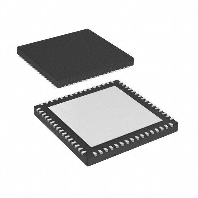
| 供应商器件封装 | 64-VQFN(9x9) |
| 其它名称 | 296-24307-2 |
| 制造商产品页 | http://www.ti.com/general/docs/suppproductinfo.tsp?distId=10&orderablePartNumber=AFE5801IRGCT |
| 功率(W) | 522mW |
| 包装 | 带卷 (TR) |
| 封装/外壳 | 64-VFQFN 裸露焊盘 |
| 标准包装 | 250 |
| 电压-电源,数字 | 1.8V,3.3V |
| 电压-电源,模拟 | 1.7 V ~ 1.9 V |
| 通道数 | 8 |


PDF Datasheet 数据手册内容提取
AFE5801 www.ti.com SLOS591D–SEPTEMBER2008–REVISEDMAY2010 8-Channel Variable-Gain Amplifier (VGA) With Octal High-Speed ADC CheckforSamples:AFE5801 FEATURES RELATED DEVICES 1 • EightVariable-GainAmplifiers(VGA) • AFE5851:16-ChannelVGA+ADC, 32.5MSPS/Channel – EightDifferentialBufferedInputsWith2Vpp MaximumSwing DESCRIPTION – 5.5nV/√HzVCAInputNoise(31dBGain) The AFE5801 is an analog front end, targeting – VariableGain,–5dBto31dBWith0.125dB applications where the power and level of integration or1dBSteps are critical. The device contains eight variable-gain – DigitalGainControl amplifiers (VGA), each followed by a high-speed (up • Third-OrderAntialiasingFilterWith to 65MSPS) ADC, for a total of eight ADCs per ProgrammableCutoffFrequency(7.5,10,or device. 14MHz) Each of the eight differential inputs is buffered, • Clamping accepts up to 2Vpp maximum input swing, and is followed by a VGA with a gain range from –5dB to • Analog-to-DigitalConverter(ADC) 31dB. The VGA gain is digitally controlled, and the – OctalChannel,12Bit,65MSPS gain curves versus time can be stored in memory – InternalandExternalReferenceSupport integratedwithinthedeviceusingtheserialinterface. – NoExternalDecouplingRequiredfor A selectable clamping and antialias low-pass filter References (with 3dB attenuation at 7.5, 10, or 14MHz) is also – SerialLVDSOutputs integratedbetweenVGAandADC,foreverychannel. • 1.8Vand3.3VSupplies The VGA/antialias filter outputs are differential • 50mWTotalPowerperChannelat30MSPS (limited to 2Vpp) and drive the onboard 12bit, 65MSPS ADC. The ADC also scales down its power • 58mWTotalPowerperChannelat50MSPS consumption should a lower sampling rate be • 64QFNPackage(9mm× 9mm) selected. The ADC outputs are serialized in LVDS streams, which further minimizes power and board APPLICATIONS area. • Imaging:Ultrasound,PET The AFE5801 is available in a 64-pin QFN package (9mm × 9mm) and is specified over the full industrial temperaturerange(–40°Cto85°C). 1 Pleasebeawarethatanimportantnoticeconcerningavailability,standardwarranty,anduseincriticalapplicationsofTexas Instrumentssemiconductorproductsanddisclaimerstheretoappearsattheendofthisdatasheet. PRODUCTIONDATAinformationiscurrentasofpublicationdate. Copyright©2008–2010,TexasInstrumentsIncorporated Products conform to specifications per the terms of the Texas Instruments standard warranty. Production processing does not necessarilyincludetestingofallparameters.
AFE5801 SLOS591D–SEPTEMBER2008–REVISEDMAY2010 www.ti.com This integrated circuit can be damaged by ESD. Texas Instruments recommends that all integrated circuits be handled with appropriateprecautions.Failuretoobserveproperhandlingandinstallationprocedurescancausedamage. ESDdamagecanrangefromsubtleperformancedegradationtocompletedevicefailure.Precisionintegratedcircuitsmaybemore susceptibletodamagebecauseverysmallparametricchangescouldcausethedevicenottomeetitspublishedspecifications. BLOCK DIAGRAM C N N EF_I C SY N LK ATA N SET OUT R G D C D E E D V T P S S S R S AVDD3 DVDD18 Time Gain Block AVDD18 Control Serial VCM Interface Memory AAF LVDS D1P IN1 ADC 1 Serializer D1M AAF D2P IN2 ADC 2 Serializer D2M AAF D3P IN3 ADC 3 Serializer D3M · · · · · · · · · · · · AAF D8P IN8 ADC 8 Serializer D8M Frame Clock FCLKP FCLKM CLKINP fCLKIN CLKINM Bit Clock DCLKP PLL 6´f DCLKM CLKIN AVSS DVSS B0328-01 2 SubmitDocumentationFeedback Copyright©2008–2010,TexasInstrumentsIncorporated ProductFolderLink(s):AFE5801
AFE5801 www.ti.com SLOS591D–SEPTEMBER2008–REVISEDMAY2010 PINOUT RGC PACKAGE (TOPVIEW) M SS DD18 SS N NC SET LK ATA N OUT SS DD18 P M C V V V C D Y E C D E D V V 1 1 V A A A N P S R S S S S D D D D 64 63 62 61 60 59 58 57 56 55 54 53 52 51 50 49 IN1P 1 48 D2P IN1M 2 47 D2M IN2P 3 46 D3P IN2M 4 45 D3M IN3P 5 44 D4P IN3M 6 43 D4M IN4P 7 42 DCLKP AFE5801 IN4M 8 41 DCLKM IN5P 9 QFN-64 40 FCLKP 9mm × 9mm IN5M 10 39 FCLKM IN6P 11 38 D5P IN6M 12 37 D5M IN7P 13 36 D6P IN7M 14 35 D6M IN8P 15 34 D7P IN8M 16 33 D7M 17 18 19 20 21 22 23 24 25 26 27 28 29 30 31 32 M 3 8 S P M S 8 N C C 8 S 8 M P VC AVDD AVDD1 AVS CLKIN CLKIN AVS AVDD1 VREF_I N N DVDD1 DVS DVDD1 D8 D8 P0056-13 TERMINALFUNCTIONS Name NUMBER DESCRIPTION AVSS 20,23,61,63 Analogground AVDD18 19,24,62 1.8Vanalogsupplyvoltage AVDD3 18 3.3Vanalogsupplyvoltage CLKINP,CLKINM 21,22 Differentialclockinputpins.Single-endedclockisalsosupported.SeetheClockInputssection. D1P/M–D8P/M 50–43,38–31 LVDSoutputsforchannels1to8 DCLKM,DCLKP 41,42 LVDSbitclockoutput DVSS 29,52 Digitalground DVDD18 28(1),30,51 1.8VLVDSbuffersupplyvoltage FCLKM,FCLKP 39,40 LVDSframeclockoutput IN1P/M–IN8P/M 1–16 Differentialanaloginputpinsforchannels1to8 NC 26,27,60 Donotconnect PDN 59 Globalpower-downcontrolinput(active-high).100kΩpulldownresistor RESET 57 Hardwareresetpin(active-high).100kΩpulldownresistor SCLK 56 Serialinterfaceclockinput.100kΩpulldownresistor SDATA 55 Serialinterfacedatainput.100kΩpulldownresistor SDOUT 53 Serialinterfacedatareadout SEN 54 Serialinterfaceenable.100kΩpullupresistor SYNC 58 TGC/VGAsynchronizationsignalinput.100kΩpulldownresistor VCM 17,64 Common-modeoutputpinsforpossiblebiasoftheanaloginputsignals VREF_IN 25 Referenceinputintheexternalreferencemode Thermalpad Bottomofpackage ConnecttoAVSS (1) Pin28canbeconnectedtothe1.8Vor3.3Vsupply,whicheveriseasierforuser.Itdoesnotaffecttheperformance. Copyright©2008–2010,TexasInstrumentsIncorporated SubmitDocumentationFeedback 3 ProductFolderLink(s):AFE5801
AFE5801 SLOS591D–SEPTEMBER2008–REVISEDMAY2010 www.ti.com PACKAGING/ORDERINGINFORMATION(1) PRODUCT PACKAGE-LEAD PACKAGE SPECIFIED PACKAGE ORDERING TRANSPORT DESIGNATOR TEMPERATURE MARKING NUMBER MEDIA, RANGE QUANTITY AFE5801 QFN-64(2) RGC –40°Cto85°C AFE5801 AFE5801IRGCT Tape/reel,250 AFE5801 QFN-64(2) RGC –40°Cto85°C AFE5801 AFE5801IRGCR Tape/reel,2000 (1) Forthemost-currentpackageandorderinginformation,seethePackageOptionAddendumattheendofthisdocument,orseetheTI Websiteatwww.ti.com. (2) Forthethermalpadsizeonthepackage,seethemechanicaldrawingsattheendofthisdocument. ABSOLUTE MAXIMUM RATINGS(1) overoperatingfree-airtemperaturerange(unlessotherwisenoted) VALUE UNIT AVDD3toAVSS –0.3to3.8 V AVDD18toAVSS –0.3to2.2 V DVDD18toDVSS –0.3to2.2 V VoltagebetweenAVSSandDVSS –0.3to0.3 V Analoginputpins(INP,INM)toAVSS –0.3VtoMIN(3.6V,AVDD3+0.3V) V i i VREF_INtoAVSS –0.3to2.2 V V ,V toAVSS –0.3to2.2 V CLKP CLKM DigitalcontrolpinstoDVSS:PDN,RESET,SCLK,SDATA,SEN,SYNC –0.3to3.6 V T Maximumoperatingjunctiontemperature 125 °C J T Storagetemperaturerange –60to150 °C stg (1) StressesbeyondthoselistedunderAbsoluteMaximumRatingsmaycausepermanentdamagetothedevice.Thesearestressratings only,andfunctionaloperationofthedeviceattheseoranyotherconditionsbeyondthoseindicatedunderRecommendedOperating Conditionsisnotimplied.Exposuretoabsolute-maximum-ratedconditionsforextendedperiodsmayaffectdevicereliability. THERMAL CHARACTERISTICS PARAMETER TESTCONDITIONS TYP UNIT q 0LFMairflow 23.17 °C/W JA q 2-oz.(0.071-mmthick)coppertraceandpadsoldereddirectlytoaJEDEC-standardfour-layer 22.1 °C/W JC 3-in.×3-in.(7.62-cm×7.62-cm)PCB. RECOMMENDED OPERATING CONDITIONS MIN TYP MAX UNIT T Ambienttemperature –40 85 °C A SUPPLIES AVDD3 Analogsupplyvoltage(VGA) 3 3.3 3.6 V AVDD18 Analogsupplyvoltage(ADC) 1.7 1.8 1.9 V DVDD18 Digitalsupplyvoltage(ADC,LVDS) 1.7 1.8 1.9 V ANALOGINPUTS INP,INM InputvoltagerangetoAVSS VCM–0.5 VCM+0.5 V i i VREF_INinexternalreferencemode 1.35 1.4 1.45 V VCMload 3 mA 4 SubmitDocumentationFeedback Copyright©2008–2010,TexasInstrumentsIncorporated ProductFolderLink(s):AFE5801
AFE5801 www.ti.com SLOS591D–SEPTEMBER2008–REVISEDMAY2010 RECOMMENDED OPERATING CONDITIONS (continued) MIN TYP MAX UNIT CLOCKINPUT f Inputclockfrequency 5 65 MSPS CLKIN Inputclockdutycycle 40% 50% 60% Sinewave,ac-coupled 0.5 Vpp V LVPECL,ac-coupled 1.6 Vpp CLKP-CLKM LVDS,ac-coupled 0.25 0.7 Vpp V LVCMOS,single-ended,V toAVSS 1.8 Vpp CLKP CLKM V High-levelinputvoltage 0.75×AVDD18 V IH V Low-levelinputvoltage 0.25×AVDD18 V IL DIGITALOUTPUT C ExternalloadcapacitancefromeachoutputpintoDVSS 5 pF LOAD R Differentialloadresistance(external)betweentheLVDSoutputpairs 100 Ω LOAD ELECTRICAL CHARACTERISTICS Typicalvaluesareat25°C,MINandMAXvaluesareacrossthefulltemperaturerangeofT =–40°CtoT =85°C, min max AVDD3=3.3V,AVDD18=1.8V,DVDD18=1.8V,–1dBFSanaloginputac-coupledwith0.1mF,internalreferencemode, maximum-ratedsamplingfrequency(65MSPS),LVCMOS(single-ended)clock,50%dutycycle,antialiasingfiltersetat 14MHz(3dBcorner),outputclampdisabled(1)andanaloghigh-passfilterenabled,unlessotherwisenoted. PARAMETER TESTCONDITIONS MIN TYP MAX UNIT VARIABLEGAINAMPLIFIER(VGA) Maximuminputvoltageswing Linearoperation,fromINPtoINM 2 Vpp VCM Common-modevoltage 1.6 V Gainrange Maximumgain–minimumgain 36 dB Maximumgain 29.5 31 32.5 dB 0.125 Gainresolution dB or1 Inputresistance Fromeachinputtodcbiaslevel 5 kΩ Inputcapacitance Differentialbetweentheinputs 2 pF ANTIALIASFILTER(AAF) 7.5MHzfilterselected 7.5 AAFcutofffrequency 10MHzfilterselected –3dB 10 MHz 14MHzfilterselected 14 7.5MHzfilterselected 10 10MHzfilterselected –6dB 14 MHz 14MHzfilterselected 20 AAFstop-bandattenuation 7.5MHzfilterselected 18 10MHzfilterselected –12dB 24 MHz 14MHzfilterselected 30 7.5MHzfilterselected 1.2 In-bandattenuation 10MHzfilterselected At3.2MHz 0.5 dB 14MHzfilterselected 0.2 (1) Enablingclampingincreasesdistortionvaluesathighswingsbyabout2dB. Copyright©2008–2010,TexasInstrumentsIncorporated SubmitDocumentationFeedback 5 ProductFolderLink(s):AFE5801
AFE5801 SLOS591D–SEPTEMBER2008–REVISEDMAY2010 www.ti.com ELECTRICAL CHARACTERISTICS (continued) Typicalvaluesareat25°C,MINandMAXvaluesareacrossthefulltemperaturerangeofT =–40°CtoT =85°C, min max AVDD3=3.3V,AVDD18=1.8V,DVDD18=1.8V,–1dBFSanaloginputac-coupledwith0.1mF,internalreferencemode, maximum-ratedsamplingfrequency(65MSPS),LVCMOS(single-ended)clock,50%dutycycle,antialiasingfiltersetat 14MHz(3dBcorner),outputclampdisabled(1)andanaloghigh-passfilterenabled,unlessotherwisenoted. PARAMETER TESTCONDITIONS MIN TYP MAX UNIT FULL-CHANNELCHARACTERISTICS Gainmatching Acrosschannelsandparts 0.1 0.6 dB –5dBto28dBgain –1.2 ±0.3 1.2 Gainerror dB Gain>28dB –1.8 ±0.5 1.8 Offseterror 31dBgain –50 50 LSB 5MHz,31dBVGAgain,low-noisemode 5 6.5 nV/√Hz Input-referrednoisevoltage 5MHz,31dBVGAgain,defaultnoisemode 5.5 nV/√Hz SNR Signal-to-noiseratio –1dBFSADCinput,6dBgain 66 dBc HD2 –1dBFSADCinput,17dBgain,f =2MHz –75 –60 in Second-harmonicdistortion dBc –1dBFSADCinput,31dBgain,f =2MHz –75 –60 in –1dBFSADCinput,17dBgain,f =2MHz –65 –55 in HD3 Third-harmonicdistortion dBc –1dBFSADCinput,31dBgain,f =2MHz –60 –52 in SFDR Spurious-freedynamicrange –1dBFSADCinput,17dBgain,f =2MHz 65 dBc in THD Totalharmonicdistortion –1dBFSADCinput,17dBgain,f =2MHz 64 dBc in IMD Intermodulationdistortion f =1MHz,f =2MHz,A =–7dBFS,30dB –70 dBFS in1 in2 in1,in2 VGAgain Groupdelayvariation f=100kHzto14MHz,acrossgainsettingsand ±3.5 ns channels f=100kHzto14MHz,acrosschannels ±1.5 Clock Inputoverloadrecovery ≤6dBoverloadtowithin1% 1 cycle Clamplevel Afteramplification.Clampenabledbydefault 3 dB ADCnumberofbits 12 Aggressor:f =3MHz,1dBbelowADCfull-scale in Crosstalk Victims(channelnexttoaggressorchannel):50Ω 92 dB differential(betweenINPandINM) i i POWER Defaultnoisemode 522 600 Totalpowerdissipation mW Low-noisemode 561 636 I AVDD3currentconsumption 6 9 mA AVDD3 I AVDD18currentconsumption Defaultnoisemode 198 222 AVDD18 mA Low-noisemode 220 244 I DVDD18currentconsumption See (2) 81 100 mA DVDD18 Standbymode 64 mW Powerdown Fullpower-downmode 8 25 mW ACPSRR Power-supplyrejectionratio 30 dBc (2) Usingdigitalmodeslikeaveraging,digitalgain,digitalHPF,etc.,(seetheApplicationInformationsection)mightincreasetheDVDD18 currentbyabout60mA. 6 SubmitDocumentationFeedback Copyright©2008–2010,TexasInstrumentsIncorporated ProductFolderLink(s):AFE5801
AFE5801 www.ti.com SLOS591D–SEPTEMBER2008–REVISEDMAY2010 DIGITAL CHARACTERISTICS(1) Thedcspecificationsrefertotheconditionwherethedigitaloutputsarenotswitching,butpermanentlyatavalidlogiclevel0 or1.Typicalvaluesareat25°C,minandmaxvaluesareacrossthefulltemperaturerangeofT =–40°CtoT =85°C, min max AVDD3=3.3V,AVDD18=1.8V,DVDD18=1.8V,externaldifferentialloadresistancebetweentheLVDSoutputpairR = LOAD 100Ω. PARAMETER TESTCONDITIONS MIN TYP MAX UNIT DIGITALINPUTS(PDN,RESET,SCLK,SDATA,SEN,SYNC) High-levelinputvoltage 1.4 3.6 V Low-levelinputvoltage 0.8 V High-levelinputcurrent 10 mA Low-levelinputcurrent 10 mA Inputcapacitance 4 pF DIGITALOUTPUTS(DP,DM) i i High-leveloutputvoltage 1375 mV Low-leveloutputvoltage 1025 mV Outputdifferentialvoltage|V | 270 380 490 mV OD OutputoffsetvoltageV Common-modevoltageofDPandDM 0.9 1.15 1.5 V OS i i Outputcapacitanceinsidethedevice,fromeitheroutputto Outputcapacitance 2 pF DVSS. DIGITALOUTPUTS(SDOUT) High-leveloutputvoltage 1.6 1.8 V Low-leveloutputvoltage 0 0.2 V Outputimpedance 50±25% Ω (1) AllLVDSspecificationshavebeencharacterizedbutnottestedatproduction.Forclockinputlevels,seetheRecommendedOperating Conditionstable. Copyright©2008–2010,TexasInstrumentsIncorporated SubmitDocumentationFeedback 7 ProductFolderLink(s):AFE5801
AFE5801 SLOS591D–SEPTEMBER2008–REVISEDMAY2010 www.ti.com OUTPUT INTERFACE TIMING Typicalvaluesareat25°C,AVDD3=3.3V,AVDD18=DVDD=1.8V,LVCMOS(singleended)clock,C =5pF,R = LOAD LOAD 100Ω,I =3.5mA,unlessotherwisenoted.MinimumandmaximumvaluesareacrossthefulltemperaturerangeT = O MIN –40°CtoT =85°C. MAX PARAMETER TESTCONDITIONS MIN TYP MAX UNIT Thedelayintimebetweentherisingedgeoftheinputsampling ta Aperturedelay clockandtheactualtimeatwhichthesamplingoccurs 0.7 3 ns Aperturedelaymatching Acrosschannelswithinthesamedevice ±150 ps tj Aperturejitter 450 fsrms TimetovaliddataaftercomingoutofSTANDBYmode 10 50 Wake-uptime TimetovaliddataaftercomingoutofPDNGLOBALmode 50 200 ms Timetovaliddataafterstoppingandrestartingtheinputclock 30 200 Input ADClatency Default,afterreset 11 clock cycles Inputclockrisingedge(zerocross)toframeclockrisingedge(zero tdelay Dataandframeclockdelay cross)minushalftheinputclockperiod(T). 3 4.7 6.4 ns Δtdelay Delayvariation Atfixedsupplyand20°CTdifference –1 1 ns Risetimemeasuredfrom–100mVto100mV tRISE Datarisetime Falltimemeasuredfrom100mVto–100mV 0.1 0.25 0.4 ns tFALL Datafalltime 10MHz<fCLKIN<65MHz Risetimemeasuredfrom–100mVto100mV tFCLKRISE Frameclockrisetime Falltimemeasuredfrom100mVto–100mV 0.1 0.25 0.4 ns tFCLKFALL Frameclockfalltime 10MHz<fCLKIN<65MHz Frameclockdutycycle Zerocrossingoftherisingedgetozerocrossingofthefallingedge 48% 50% 52% Risetimemeasuredfrom–100mVto100mV tDCLKRISE Bitclockrisetime Falltimemeasuredfrom100mVto–100mV 0.1 0.2 0.35 ns tDCLKFALL Bitclockfalltime 10MHz<fCLKIN<65MHz Zerocrossingoftherisingedgetozerocrossingofthefallingedge Bitclockdutycycle 44% 50% 56% 10MHz<fCLKIN<65MHz Output Interface Timing(1) fCLKIN,InputClockFrequency Period(T) SetupTnisme(tsu), HoldTnimse(th), tpdi=0.5×T+tdelay,ns InputClockZero-Cross(rising Zero-CrossDatatoZero-Cross Zero-CrossClocktoZero-Cross edge)toFrameClockZero-Cross MHz ns Clock(bothedges) Data(bothedges) (risingedge) MIN TYP MAX MIN TYP MAX MIN TYP MAX 65 15 0.35 0.6 0.3 0.6 12.3 50 20 0.5 0.8 0.5 0.8 14.6 40 25 0.75 1 0.75 1 17 30 33 1 1.4 1 1.4 21.2 20 50 1.7 2.1 1.7 2.1 29.5 10 100 3.8 4.2 3.8 4.2 54.7 (1) FCLKtimingisthesameasfortheoutputdatalines.IthasthesamerelationtoDCLKasthedatapins.Setupandholdarethesame forthedataandtheframeclock. 8 SubmitDocumentationFeedback Copyright©2008–2010,TexasInstrumentsIncorporated ProductFolderLink(s):AFE5801
AFE5801 www.ti.com SLOS591D–SEPTEMBER2008–REVISEDMAY2010 D11D10(D(D0)1) SAMPLEN + 1 T0434-01 D0(D11) D1(D10) D2(D9) D3(D8) D4(D7) SampleN + 11 T D5D6(D6)(D5) SAMPLEN D7(D4) D8(D3) D9(D2) D10(D1) D11(D0) D0(D11) D1(D10) th tpdi D2D3(D9)(D8) tsu + 1 D4(D7) Dn SampleN + 10 D5D6(D6)(D5) SAMPLEN–1 D7(D4) D8(D3) Dn D9(D2) th D10(D1) D11(D0) KP KM tsu out CyclesLatency D0(D11) DCL DCL CHi 11Clock DDD321(D8)(D9)(D10) Bit Clock ut Data Pair D4(D7) utp SampleN ta D5D6(D6)(D5) SAMPLEN–11 O D7D8(D4)(D3) MSBFirstMode LSBFirstMode D9(D2) Bitin Bitin D10(D1) Data Data D11(D0) D0(D11) D13(D2) D1(D10) InputSignal InputClockCLKINFreq = fCLKIN FrameClockFCLKFreq=fCLKIN BitClockDCLKFreq=6xfCLKIN OutputDataChOUTnDatarate=12xfCLKIN Figure1. TimingDiagram Copyright©2008–2010,TexasInstrumentsIncorporated SubmitDocumentationFeedback 9 ProductFolderLink(s):AFE5801
AFE5801 SLOS591D–SEPTEMBER2008–REVISEDMAY2010 www.ti.com TYPICAL CHARACTERISTICS Allgraphsareat25°C,AVDD3=3.3V,AVDD18=DVDD18=1.8V,–1dBFSanaloginputACcoupledwith0.1mF,internal referencemode,maximumratedchannelsamplingfrequency(65MSPS),LVCMOS(single-ended)clock,50%dutycycle, f =2MHz,anti-aliasingfiltersetat14MHz(3dBcorner),outputclampdisableandanaloghigh-passfilterenabled.spacer IN 10 10 Ain = −1dBFS Ain = −1dBFS Gain = 12dB Gain = 30dB −10 HD2 = −80.1dBc −10 HD2 = −69.8dBc HD3 = −64.2dBc HD3 = −59.5dBc B −30 SFDR = 63.9dBc B −30 SFDR = 59.5dBc − d SNR = 65.9dBFS − d SNR = 58.8dBFS e THD = 63.9dBc e THD = 58.9dBc ud −50 ud −50 plit plit m m A −70 A −70 −90 −90 −110 −110 0 5 10 15 20 25 30 35 0 5 10 15 20 25 30 35 f − Frequency − MHz f − Frequency − MHz G001 G002 Figure2.FFTfor2MHzInputSignaland12dBGain Figure3.FFTfor2MHzInputSignaland30dBGain 32 32 30 Coarse Gain = 31dB 28 85°C 28 24 26 −40°C 24 20 B B Gain − d 122802 Coarse Gain = 19dB Gain − d 1126 (Ideal+1dB) Line 25°C − 16 − 8 G G 14 4 12 0 10 (Ideal−1dB) Line 8 Coarse Gain = 7dB −4 6 −8 0.000 0.125 0.250 0.375 0.500 0.625 0.750 0.875 0 4 8 12 16 20 24 28 32 36 FINE_GAIN Register Setting Gain Code G021 G025 Figure4.FineGainvsGainCode Figure5.GainvsGainCodeandTemperature 1.0 185 0.8 Hz 165 Low-Noise Enabled 0.6 √ V/ dB 0.4 −40°C 25°C e − n 145 Gain Error − −000...022 eferred Nois 110255 Low-Noise Disabled −0.4 R 85 −0.6 put- −0.8 85°C Out 65 −1.0 45 −5 0 5 10 15 20 25 30 −5 0 5 10 15 20 25 30 G − Gain − dB G − Gain − dB G026 G022 Figure6.GainErrorvsGainCodeandTemperature Figure7.Output-ReferredNoisevsGain 10 SubmitDocumentationFeedback Copyright©2008–2010,TexasInstrumentsIncorporated ProductFolderLink(s):AFE5801
AFE5801 www.ti.com SLOS591D–SEPTEMBER2008–REVISEDMAY2010 TYPICAL CHARACTERISTICS (continued) Allgraphsareat25°C,AVDD3=3.3V,AVDD18=DVDD18=1.8V,–1dBFSanaloginputACcoupledwith0.1mF,internal referencemode,maximumratedchannelsamplingfrequency(65MSPS),LVCMOS(single-ended)clock,50%dutycycle, f =2MHz,anti-aliasingfiltersetat14MHz(3dBcorner),outputclampdisableandanaloghigh-passfilterenabled.spacer IN 98 11 88 z z 10 H H √ 78 √ nV/ nV/ 9 − 68 − oise 58 Low-Power Mode Enabled oise 8 Low-Power Mode Disabled N N ed 48 ed 7 Referr 38 Referr 6 put- 28 put- Low-Power Mode Enabled n n 5 I 18 Low-Power Mode Disabled I 8 4 −6 −4 −2 0 2 4 6 8 10 12 14 16 18 17 18 19 20 21 22 23 24 25 26 27 28 29 30 31 G − Gain − dB G − Gain − dB G023 G024 Figure8.Input-ReferredNoiseforLowGains Figure9.Input-ReferredNoiseforHighGains −60 −70 Ain = −1dBFS −72 Ain = −6dBFS −65 fIN = 10MHz −74 fIN = 10MHz −76 −70 Bc Bc −78 d d − −75 − −80 2 2 HD HD −82 −80 −84 fIN = 5MHz −85 −86 fIN = 5MHz fIN = 1MHz −88 fIN = 1MHz −90 −90 −10 0 10 20 30 40 −10 0 10 20 30 40 G − Gain − dB G − Gain − dB G003 G004 Figure10.HD2AcrossCoarseGainandThreef Figure11.HD2AcrossCoarseGainandThreef IN IN (–1dBFS)(1) (–6dBFS)(2) (1) Forgains≥5dB,theinputamplitudeisadjustedtogive–1dBFS.At5dBgain,inputamplitudeis4dBm(correspondingto–1dBFS). Forgainslessthan5dB,theinputiskeptconstantat4dBm. (2) Forgains≥0dB,theinputamplitudeisadjustedtogive–6dBFS.At0dBgain,inputamplitudeis4dBm(correspondingto–6dBFS). Forgainslessthan0dB,theinputiskeptconstantat4dBm. Copyright©2008–2010,TexasInstrumentsIncorporated SubmitDocumentationFeedback 11 ProductFolderLink(s):AFE5801
AFE5801 SLOS591D–SEPTEMBER2008–REVISEDMAY2010 www.ti.com TYPICAL CHARACTERISTICS (continued) Allgraphsareat25°C,AVDD3=3.3V,AVDD18=DVDD18=1.8V,–1dBFSanaloginputACcoupledwith0.1mF,internal referencemode,maximumratedchannelsamplingfrequency(65MSPS),LVCMOS(single-ended)clock,50%dutycycle, f =2MHz,anti-aliasingfiltersetat14MHz(3dBcorner),outputclampdisableandanaloghigh-passfilterenabled.spacer IN −30 −40 −35 Ain = −1dBFS Ain = −6dBFS −50 fIN = 5MHz −40 fIN = 10MHz −60 fIN = 1MHz dBc −45 fIN = 1MHz fIN = 10MHz dBc − −50 − −70 3 fIN = 5MHz 3 D D H −55 H −80 −60 −90 −65 −70 −100 −10 0 10 20 30 40 −10 0 10 20 30 40 G − Gain − dB G − Gain − dB G005 G006 Figure12.HD3AcrossCoarseGainandThreef Figure13.HD3AcrossCoarseGainandThreef IN IN (–1dBFS)(1) (–6dBFS)(2) −20 −30 −30 fIN = 2MHz −40 fIN = 2MHz −40 Gain = 30dB Gain = 30dB −50 −50 dB dB −60 2 − −60 3 − D D −70 H −70 Gain = 6dB H −80 −80 Gain = 18dB Gain = 18dB −90 −90 Gain = 6dB −100 −100 −70 −60 −50 −40 −30 −20 −10 0 −70 −60 −50 −40 −30 −20 −10 0 Output Amplitude − dBFS Output Amplitude − dBFS G007 G008 Figure14.HD2vsOutputAmplitude Figure15.HD3vsOutputAmplitude −60 2090 −70 2080 Analog HPF Disabled e d Bc −80 3MHz − Adjacent 3MHz − Far Co 2070 Analog HPF Enabled Amplitude − d −−19000 utput Offset − 22005600 O −110 10MHz − Adjacent 2040 Digital HPF Enabled 10MHz − Far −120 2030 0 2 4 6 8 10 −5 0 5 10 15 20 25 30 Channel G − Gain − dB G009 G027 Figure16.Crosstalk(3) Figure17.OutputOffsetvsGain (3) –1dBsignalappliedononechannelatatimeandoutputisobservedon: 1.Adjacentchannel-channelnexttotheaggressorchannel,butnotasharedchannel 2.Farchannel-allotherchannels(neithersharedoradjacent) 12 SubmitDocumentationFeedback Copyright©2008–2010,TexasInstrumentsIncorporated ProductFolderLink(s):AFE5801
AFE5801 www.ti.com SLOS591D–SEPTEMBER2008–REVISEDMAY2010 TYPICAL CHARACTERISTICS (continued) Allgraphsareat25°C,AVDD3=3.3V,AVDD18=DVDD18=1.8V,–1dBFSanaloginputACcoupledwith0.1mF,internal referencemode,maximumratedchannelsamplingfrequency(65MSPS),LVCMOS(single-ended)clock,50%dutycycle, f =2MHz,anti-aliasingfiltersetat14MHz(3dBcorner),outputclampdisableandanaloghigh-passfilterenabled.spacer IN 1 20 0 10 K = 7dB Analog Filter −1 14MHz B d −2 0 − de −3 B −10 mplitu −−54 n − d −20 K = 4dB K = 2dB alized A −−−876 7.5MHz G − Gai −−4300 K = K6d =B 5dB K = 3dB m Nor −9 10MHz −50 K = 8dB −10 −60 K = 9dB −11 K = 10dB −12 −70 0 2 4 6 8 10 12 14 16 18 20 0.0 0.5 1.0 1.5 2.0 2.5 3.0 fIN − Input Frequency − MHz G010 f − Frequency − MHz G011 Figure18.AntialiasingFilterFrequencyResponse Figure19.High-PassFilterOptions 450 0.60 400 AVDD Power − Low-Noise Mode fin = 2MHz 0.55 350 W W Total Power − Low-Noise Mode wer − m 235000 AVDD Power − Default wer − m 0.50 3 Po 200 al Po 0.45 DD 150 Tot 0.40 AV 100 P − 0.35 Total Power − Default 50 fIN = 2MHz 0 0.30 0 10 20 30 40 50 60 70 5 10 15 20 25 30 35 40 45 50 55 60 65 f − Clock Frequency − MSPS f − Clock Frequency − MSPS G012 G013 Figure20.AnalogPowervsInput-ClockFrequency Figure21.TotalPowervsInput-ClockFrequency 7 4.0 6 % 3.5 − s) 3.0 5 el % nn s − 4 Cha 2.5 currence 3 mber of 12..50 O u 2 N nt ( 1.0 1 Cou 0.5 0 0.0 0.02 0.07 0.12 0.17 0.22 0.27 0.32 0.37 0.42 0.47 0.52 2005 2016 2027 2038 2049 2060 2071 2072 2083 GAIN_MATCHING − dB Output Code − Offset G030 G031 Figure22.GainMatchingMeasuredataSingleGain(30 Figure23.Offset(AverageCode)WithSignal.Every dB)asPeak-to-PeakVariationofGainAcrossChannels ChannelCountedasOneEvent onEveryDeviceandMeasuredatThreeTemperatures. EveryDeviceatEachTemperatureCountedasOneEvent Copyright©2008–2010,TexasInstrumentsIncorporated SubmitDocumentationFeedback 13 ProductFolderLink(s):AFE5801
AFE5801 SLOS591D–SEPTEMBER2008–REVISEDMAY2010 www.ti.com TYPICAL CHARACTERISTICS (continued) Allgraphsareat25°C,AVDD3=3.3V,AVDD18=DVDD18=1.8V,–1dBFSanaloginputACcoupledwith0.1mF,internal referencemode,maximumratedchannelsamplingfrequency(65MSPS),LVCMOS(single-ended)clock,50%dutycycle, f =2MHz,anti-aliasingfiltersetat14MHz(3dBcorner),outputclampdisableandanaloghigh-passfilterenabled.spacer IN 2800 2600 fIN = 2MHz 2400 e 2200 d o C 2000 put 1800 ut O 1600 1400 1200 1000 0 1000 2000 3000 4000 5000 6000 7000 8000 Sample G014 Figure24.TGCSweepWithInterpolationDisabledandHigh-PassFilterEnabled 2800 2600 fIN = 2MHz 2400 e 2200 d o C 2000 put 1800 ut O 1600 1400 1200 1000 0 1000 2000 3000 4000 5000 6000 7000 8000 Sample G015 Figure25.TGCSweepWithInterpolationDisabledandHigh-PassFilterDisabled 2800 2600 fIN = 2MHz 2400 e 2200 d o C 2000 put 1800 ut O 1600 1400 1200 1000 2500 3500 4500 5500 6500 7500 8500 9500 Sample G016 Figure26.TGCSweepWithInterpolationEnabledandHigh-PassFilterDisabled 14 SubmitDocumentationFeedback Copyright©2008–2010,TexasInstrumentsIncorporated ProductFolderLink(s):AFE5801
AFE5801 www.ti.com SLOS591D–SEPTEMBER2008–REVISEDMAY2010 TYPICAL CHARACTERISTICS (continued) Allgraphsareat25°C,AVDD3=3.3V,AVDD18=DVDD18=1.8V,–1dBFSanaloginputACcoupledwith0.1mF,internal referencemode,maximumratedchannelsamplingfrequency(65MSPS),LVCMOS(single-ended)clock,50%dutycycle, f =2MHz,anti-aliasingfiltersetat14MHz(3dBcorner),outputclampdisableandanaloghigh-passfilterenabled.spacer IN 0 Gain = 30dB −20 fIN1 = 2.92MHz at −7dBFS B fIN2 = 3.12MHz at −7dBFS d −40 IMD3 = −70dBFS − e d −60 u plit m −80 A −100 −120 0 5 10 15 20 25 30 35 f − Frequency − MHz G017 Figure27.IntermodulationDistortion 21 67 19 Gain = 30dB 66 z H Analog HPF Disabled √ 17 65 nV/ fIN = 1MHz ed Noise − 111135 Default R − dBFS 666234 fIN = 5MHz fIN = 10MHz eferr 9 High-Pass Digital Filter K = 4 SN 61 R ut- 7 60 p n I 5 59 Ain = −1dBFS 3 58 0.0 0.5 1.0 1.5 2.0 2.5 3.0 −10 0 10 20 30 40 f − Frequency − MHz G − Gain − dB G018 G019 Figure28.Input-ReferredNoisevsFrequency Figure29.SNRvsGain,Threef (–1dBFS) IN 67 1 66 fS = 65MSPS 0 Low-Pass Filter = 14MHz B 65 d Low-Noise Mode Enabled fIN = 1MHz − −1 R − dBFS 666234 fIN = 5MHzfIN = 10MHz d Amplitude −−32 Gain = −G6daBin = 30dB Gain = G6daBin = 12dB N e S 61 maliz −4 Gain = 0dB 60 or Gain = 24dB N −5 59 Gain = 18dB Ain = −6dBFS 58 −6 −10 0 10 20 30 40 0.0 0.2 0.4 0.6 0.8 1.0 1.2 1.4 1.6 1.8 2.0 G − Gain − dB Normalized Frequency − f/fc G020 G028 Figure30.SNRvsGainThreef (–6dBFS) Figure31.LPFResponseAcrossCoarseGain IN Copyright©2008–2010,TexasInstrumentsIncorporated SubmitDocumentationFeedback 15 ProductFolderLink(s):AFE5801
AFE5801 SLOS591D–SEPTEMBER2008–REVISEDMAY2010 www.ti.com TYPICAL CHARACTERISTICS (continued) Allgraphsareat25°C,AVDD3=3.3V,AVDD18=DVDD18=1.8V,–1dBFSanaloginputACcoupledwith0.1mF,internal referencemode,maximumratedchannelsamplingfrequency(65MSPS),LVCMOS(single-ended)clock,50%dutycycle, f =2MHz,anti-aliasingfiltersetat14MHz(3dBcorner),outputclampdisableandanaloghigh-passfilterenabled.spacer IN 1 0 fS = 65MSPS 0 Low-Pass Filter = 14MHz B d Low-Noise Mode Disabled − −1 e d Gain = 6dB u plit −2 Gain = −6dB DCLK m Gain = 12dB A d −3 Gain = 30dB e maliz −4 Gain = 0dB or Gain = 24dB N −5 Gain = 18dB Data −6 0.0 0.2 0.4 0.6 0.8 1.0 1.2 1.4 1.6 1.8 2.0 Normalized Frequency − f/fc G029 Figure32.LPFResponseAcrossCoarseGain Figure33.LVDSEyePattern 16 SubmitDocumentationFeedback Copyright©2008–2010,TexasInstrumentsIncorporated ProductFolderLink(s):AFE5801
AFE5801 www.ti.com SLOS591D–SEPTEMBER2008–REVISEDMAY2010 APPLICATION INFORMATION THEORY OF OPERATION The AFE5801 is a very low-power CMOS monolithic analog front end which includes an eight-channel variable-gainamplifier(VGA)followedbyaneight-channel,12bit,high-speedpipelineanalog-to-digitalconvereter (ADC)basedonswitched-capacitorarchitecture. Each of the eight VGA differential inputs is buffered and accepts a maximum swing of 2Vpp centered at a dc level(VCM)ofabout1.6V. Each VGA has a gain range from –5dB to 31dB, and the gain is digitally controlled, with a resolution of 0.125dB. Using the serial interface, the gain curves (common to all VGAs) versus time can be stored in the memory integratedwithinthedevice. A hardware sync input pin is available (SYNC). When a pulse is applied to this pin, all the VGAs in the device start stepping through the selected time-gain curve at the same clock cycle. This sync can also be initiated by softwareusingtheserialinterface. Aselectableanti-aliaslow-passfilter(AAF)with3dBattenuationat7.5MHz,10MHz,or14MHzisalsointegrated, togetherwithclamping(whichcanbedisabled). The VGA/AAF can output 2Vpp differential swing without degradation in the specified linearity and can drive an onboard 12bit ADC. After the input signals are captured by the sample-and-hold circuit, at the rising edge of the clock, the samples are sequentially converted by a series of low-resolution stages. The outputs of the stages are combined in a digital correction logic block to form the final 12bit word with a latency of 11 clock cycles, without taking into account the delays introduced by the optional digital signal-processing functions. These functions are, in this order, offset correction, channel averaging, digital gain, and high-pass filtering (see General-Purpose Register Map for more details). The 12bit words of each channel are serialized and output as LVDS levels. For slower operation speeds, the AFE5801 offers the possibility of multiplexing up to two input channels into one LVDS output stream, reducing even further the power consumption and routing area. In addition to the data streams,abitclockandframeclockarealsooutput.Theframeclockisalignedwiththe12bitwordboundary. Notice that for the correct operation of the device (see the Serial Interface section), a positive pulse must be applied to the RESET pin. This sets the internal control registers to zero. There is, nevertheless, no need for any typeofpower-upsequencing. INPUT CONFIGURATION The analog input for the AFE5801, Figure 34, consists of a differential analog buffer which has inputs biased to 1.6V (usually refered as common-mode voltage, V ). The biasing is done with two internal resistors of 5kΩ. For CM proper operation, the input signal should be either ac-coupled or have a commn-mode value equal to V . In the CM case of ac coupling, the external input capacitors form a high-pass filter with the internal bias resistors (5kΩ), so, the value of the capacitors should allow the lowest frequency of interest to pass with minimum attenuation. For the typical frequencies used in ultrasound (>1MHz) a value of 10nF or bigger is recommended. If dc coupling is preferred,theusercantaptheV outputpinstosetthecommon-modeleveloftheinputsignal.TheV output CM CM should be connected to high-input-impedance circuits, as its driving capability is limited. Regardless of the chooseninputconfiguration,acapacitorof100nFshouldbeconnectedoneachV inputtoAVSS. CM For proper operation, the input signal should be in the recommended input range. The maximum input swing is limited to 2Vpp before saturation/distortion fo the input stage occurs. As the input common mode (VCM) is about 1.6V,eachinputofthebuffershouldstaybetween1.1Vand2.1V. Copyright©2008–2010,TexasInstrumentsIncorporated SubmitDocumentationFeedback 17 ProductFolderLink(s):AFE5801
AFE5801 SLOS591D–SEPTEMBER2008–REVISEDMAY2010 www.ti.com INP 5 kW Channel Vcm AC Clamp Input Coupling 5 kW INM CM Buffer Internal Voltage Reference NOTE: Dashedareadenotesoneofeightchannels. Figure34. Common-ModeBiasingofInputPins Themaximuminputswingislimitedto2Vppbeforedistortion/saturationoftheinputstageoccurs.Astheinputdc level(VCM)isabout1.6V,thismeansthateachinputoftheVGAtypicallystaysbetween1.1Vand2.1V. To drive the AFE5801 with a single-ended signal, the signal should be connected to one of the inputs (INP, in i principle, to keep the polarity) and the other connected to AVSS through a 100nF capacitor. In fact, all the AFE5801 inputs that must be connected to ground can be shorted together and connected to ground through a single 100nF capacitor. The input is limited to 1Vpp (from 1.1V to 2.1V) and the performance is similar to that of the AFE5851. Every channel on the AFE5851 is similar to a channel on the AFE5801 where the other input has been shorted internally to VCM. See the AFE5851 16 Channel Variable Gain Amplifier (VGA) With Octal High SpeedADCdatasheet(SLOS574)formoreinformation. SERIAL INTERFACE RegisterInitialization After power up, the internal registers must be initialized to the default value (zero). Initialization can be done in oneoftwoways: • Throughahardwarereset,byapplyingapositivepulseintheRESETpin • Through a software reset, using the serial interface, by setting the SOFTWARE RESET bit to high. Setting this bit initializes the internal registers to the respective default values (all zeros) and then self-resets the SOFTWARERESETbittolow.Inthiscase,theRESETpincanstaylow(inactive). It is important to notice that after power up and before the device is reset to its default state, the power consumptioncouldbeupto2×thespecifiedmaximum,duetotheunknownsettingoftheinternalregisters.In order to prevent the initial increased power consumption, a potential solution is to connect the RESET pin to either 1.8V or 3.3V supply with a 10kΩ resistor, so that the device is reset while powering up. For the reset to take effect, the power must be up on DVDD18. Notice that there is no damage to the part by applying voltage totheRESETpinwhilethedevicepowerisoff. Notice also that the reset only affects the digital registers, putting the part in its default state. It does not act as a power down and as such, everything internal just keeps running. As the internal registers change their values, the effects on the data propagate through the pipe. At the same time, there may be some glitches on the output due to the transition of the registers values if any of the output controlling modes, for instance, change. As the reset is level-sensitive and asynchronous with the input clock, it should be inactive in order to write into the internal registers. Although it takes only 10ns after the reset rising edge to change the registers, the output data may take, in the worst case, up to 20 clock cycles to be considered stable. Notice that the output clocks (data and frame) are independent of the RESET and tight to the input clock, avoiding any loss ofsynchronization. 18 SubmitDocumentationFeedback Copyright©2008–2010,TexasInstrumentsIncorporated ProductFolderLink(s):AFE5801
AFE5801 www.ti.com SLOS591D–SEPTEMBER2008–REVISEDMAY2010 ResetTiming Typical values at 25°C, min and max values across the full temperature range T = –40°C to T = 85°C, MIN MAX AVDD3=3.3V,AVDD18=DVDD18=1.8V,unlessotherwisenoted. PARAMATER CONDITIONS MIN TYP MAX UNIT Delayfrompower-upofAVDDandLVDDtoRESETpulse t Power-ondelaytime 5 ms 1 active t Resetpulsewidth PulsewidthofactiveRESETsignal 10 ns 2 t Registerwritedelaytime DelayfromRESETdisabletoSENactive 25 ns 3 t Power-updelaytime Delayfrompower-upofAVDDandLVDDtooutputstable 6.5 ms PO Power Supply AVDD, LVDD t 1 RESET t 2 t 3 SEN T0108-04 Figure35. ResetTiming Programming of different modes can be done through the serial interface formed by pins SEN (serial interface enable), SCLK (serial interface clock), SDATA (serial interface data) and RESET. SCLK and SDATA have a 100kΩ pulldown resistor to ground, and SEN has a 100kΩ pullup resistor to DVDD18. Serial shift of bits into the device is enabled when SEN is low. Serial data SDATA is latched at every rising edge of SCLK when SEN is active (low). The serial data is loaded into the register at every 24th SCLK rising edge when SEN is low. In case the word length exceeds a multiple of 24 bits, the excess bits are ignored. Data can be loaded in multiples of 24bit words within a single active SEN pulse (there is an internal counter that counts groups of 24 clocks after the falling edge of SEN). The interface can work with SCLK frequency from 20MHz down to very low speeds (a fewHertz)andevenwithanon-50%duty-cycleSCLK. The data is divided in two main portions: a register address (8 bits) and the data itself, to load on the addressed register (16 bits). When writing to a register with unused bits, these should be set to 0. Also, when writing, the SDOUTsignaloutputszeros.Thefollowingtimingdiagramillustratesthisprocess. Copyright©2008–2010,TexasInstrumentsIncorporated SubmitDocumentationFeedback 19 ProductFolderLink(s):AFE5801
AFE5801 SLOS591D–SEPTEMBER2008–REVISEDMAY2010 www.ti.com Start Sequence End Sequence SEN t 6 t1 t7 t 2 Data Latched On Rising Edge of SCLK SCLK t 3 SDATA A7 A6 A5 A4 A3 A2 A1 A0 D15 D14 D13 D12 D11 D10 D9 D8 D7 D6 D5 D4 D3 D2 D1 D0 t 4 t 5 Start Sequence End Sequence RESET T0384-01 Figure36. SerialInterfaceRegisterWrite Minimum values across full temperature range T = –40°C to T = 85°C, AVDD3 = 3.3V, AVDD18 = MIN MAX DVDD18=1.8V. PARAMETER DESCRIPTION MIN TYP MAX UNIT t SCLKperiod 50 ns 1 t SCLKhightime 20 ns 2 t SCLKlowtime 20 ns 3 t Datasetuptime 5 ns 4 t Dataholdtime 5 ns 5 t SENfalltoSCLKrise 8 ns 6 t TimebetweenlastSCLKrisingedgetoSENrisingedge 8 ns 7 GENERAL-PURPOSE REGISTER MAP The internal registers can be divided in two groups, a group of registers to control all the general functions and settings of the device, and a bank of registers to control the TGC/gain curves operation. Those two sets of registers overlap in all the address space, except for the address 0, which holds the control of the register bank. One of the bits of this register, TGC_REG_WREN (see following table) is used to access one set of registers or the other. Its default value is zero and gives access to the general-purpose registers (which are also by default zero). The TGC control registers (described after the general-purpose registers) can be accessed by writing 1 to TGC_REG_WREN. The following table describes the function of the registers when TGC_REGISTER_WREN = 0 (default). The addressformatisaddress[bitoftheregister]. ADDRESS FUNCTION DESCRIPTION 0[2] TGC_REGISTER_WREN 0:Accesstogeneral-purposeregisters.1:AccesstoTGCregisters 0[1] REGISTER_READOUT_ENABLE 1:Enablesreadoutoftheregisters 0[0] SOFTWARE_RESET 1:Resetsthedeviceandself-resetsthebittozero 1[14] OUTPUT_RATE_2X 0:1×rate(oneADCperLVDSstream).1:2×rate(2ADCsperLVDSstream) 1[13] EXTERNAL_REFERENCE 0:Internalreference.1:Externalreference 1[11] LOW_FREQUENCY_NOISE_SUPRESSION 0:Nosupression.1:Supressesnoiseatlowfrequenciesandpushesittof /2 S 20 SubmitDocumentationFeedback Copyright©2008–2010,TexasInstrumentsIncorporated ProductFolderLink(s):AFE5801
AFE5801 www.ti.com SLOS591D–SEPTEMBER2008–REVISEDMAY2010 ADDRESS FUNCTION DESCRIPTION 1[10] STDBY 0:Powerup.1:Standby(fastpower-upmode) 1[9:2] PDNCHANNEL<7:0> PDNforeachindividualchannel(VCA+ADC).LVDSoutputslogic0. 1[1] OUTPUT_DISABLE 0:Ouptutenabled.1:Outputdisabled 1[0] GLOBAL_PDN 0:Powerup.1:Globalpowerdown(slowpower-upmode) 2[15:13] PATTERN_MODES PatternmodesforserialLVDS.000:Nopattern.001:Sync.010:Deskew. 011:Customreg.100:All1s.101:toggle.110:All0s.111:Ramp 2[11] AVERAGING_ENABLE 0:Default(noaveraging).1:AveragetwochannelstoincreaseSNR. 2[10:3] PDN_LVDS Powerdowntheeightdata-outputLVDSpairs. 3[14:13] SERIALIZED_DATA_RATE Serializationfactor.00:12×.01:10×.10:16×.11:14× 3[12] DIGITAL_GAIN_ENABLE 0:Default(nogain).1:Applydigitalgainsetbythefollowingregisters. 3[8] REGISTER_OFFSET_SUBTRACTION_ 0:Default(nosubtraction).1:Subtractoffsetvaluesetinthecorresponding ENABLE registers. 4[3] DFS Dataformatselect.0:2scomplement.1:Offsetbinary 5[13:0] CUSTOM_PATTERN CustompatterndataforLVDS(PATTERN_MODES=011) 7[10] VCA_LOW_NOISE_MODE_(INCREASE_ 0:Lowpower.1:Lownoise,attheexpenseofincreasedpower(5mW/channel) POWER) 7[8:7] SELF_TEST 00or10:Noself-test.01:Self-testenabled.100mVdcappliedtotheinputof thechannels.11:Self-testenabled.150mVdcappliedtotheinputofthe channels.NOTE:DCappliedbeforetheinputbuffer.Testdoesnotworkifinput isdc-shortedtoadifferentpotential.Alsonoticethatthe INTERNAL_AC_COUPLINGbitisautomaticallysetto1whenenteringthis mode,andresetbacktowhatevervalueithadbefore,whenleavingthismode. 7[3:2] FILTER_BW 00:14MHz.01:10MHz.10:7.5MHz.11:Notused. 7[1] INTERNAL_AC_COUPLING VGAcoupling.0:AC-coupled.1:DC-coupled 13[15:11] DIG_GAIN1 0dBto6dBinstepsof0.2dB 13[9:2] OFFSET_CH1 Valuetobesubtractedfromchannel1 15[15:11] DIG_GAIN2 0dBto6dBinstepsof0.2dB 15[9:2] OFFSET_CH2 Valuetobesubtractedfromchannel2 17[15:11] DIG_GAIN3 0dBto6dBinstepsof0.2dB 17[9:2] OFFSET_CH3 Valuetobesubtractedfromchannel3 19[15:11] DIGGAIN4 0dBto6dBinstepsof0.2dB 19[9:2] OFFSET_CH4 Valuetobesubtractedfromchannel4 21[4:1] DIGITAL_HIGH_PASS_FILTER_CORNER_ Setskforthehigh-passfilterasdesribedinGeneral-PurposeRegister FREQ_FOR_CHANNELS-1–4 Description(kfrom2to10). 21[0] DIGITAL_HIGH_PASS_FILTER_ENABLE_ 0:Nohigh-passfilter.1:High-passfilterenabled FOR_CHANNELS_1–4 25[15:11] DIG_GAIN8 0dBto6dBinstepsof0.2dB 25[9:2] OFFSET_CH8 Valuetobesubtractedfromchannel5 27[15:11] DIG_GAIN7 0dBto6dBinstepsof0.2dB 27[9:2] OFFSET_CH7 Valuetobesubtractedfromchannel6 29[15:11] DIG_GAIN6 0dBto6dBinstepsof0.2dB 29[9:2] OFFSET_CH6 Valuetobesubtractedfromchannel7 31[15:11] DIG_GAIN5 0dBto6dBinstepsof0.2dB 31[9:2] OFFSET_CH5 Valuetobesubtractedfromchannel8 33[4:1] DIGITAL_HIGH_PASS_FILTER_CORNER_ Setskforthehigh-passfilterasdesribedinGeneral-PurposeRegister FREQ_FOR_CHANNELS_5–8 Description(kfrom2to10). 33[0] DIGITAL_HIGH_PASS_FILTER_ENABLE_ 0:Nohigh-passfilter.1:High-passfilterenabled FOR_CHANNELS_5–8 70[14] CLAMP_DISABLE 0:Enabled.1:Disabled Copyright©2008–2010,TexasInstrumentsIncorporated SubmitDocumentationFeedback 21 ProductFolderLink(s):AFE5801
AFE5801 SLOS591D–SEPTEMBER2008–REVISEDMAY2010 www.ti.com GENERAL-PURPOSE REGISTER DESCRIPTION AVERAGING_ENABLE Address:2[11] When set to 1, two samples, corresponding to two consecutive channels, are averaged (channel 1 with 2, 3 with 4, 5 with 6, and 7 with 8). If both channels receive the same input, the net effect is an improvement in SNR.Theaveragingisperformedas: • Channel1+channel2comesoutonchannel3. • Channel3+channel4comesoutonchannel4. • Channel5+channel6comesoutonchannel5. • Channel7+channel8comesoutonchannel6. DFS Address:4[3] DFS stands for data format select. The ADC output, by default, is in 2s-complement mode. Programming the DFSbitto1invertstheMSB,andtheoutputbecomesstraight-offsetbinarymode. DIGITAL_GAIN_ENABLE Address:3[12] Setting this bit to 1 applies to each channel i the corresponding gain given by DIG_GAIN<15:11>. The gain i is given as 0dB + 0.2dB × DIG_GAIN<15:11>. For instance, if DIG_GAIN <15:11> = 3, channel 5 is i 5 increased by 0.6dB gain. DIG_GAIN<15:11> = 31 produces the same effect as DIG_GAIN<15:11> = 30, i i settingthegainofchannelito6dB. DIGITAL_HIGH_PASS_FILTER_ENABLEandDIGITAL_HIGH_PASS_FILTER_CORNER_FREQ DIGITAL_HIGH_PASS_FILTER_ENABLE(channels1–4):Address:21[0] DIGITAL_HIGH_PASS_FILTER_ENABLE(channels5–8):Address:33[0] DIGITAL_HIGH_PASS_FILTER_CORNER_FREQ(channels1–4):Address:21[4:1] DIGITAL_HIGH_PASS_FILTER_CORNER_FREQ(channels5–8):Address:33[4:1] This group of four registers controls the characteristics of a digital high-pass transfer function applied to the output data, following the formula: y(n) = 2k/(2k + 1) [x(n) – x(n – 1) + y(n – 1)]. The DIGITAL_HIGH_PASS_FILTER_CORNER_FREQ registers (one for the first four channels and one for the secondgroupoffourchannels)describethesettingofk. EXTERNAL_REFERENCE Address:1[13] The internal reference mode (default) uses approximately 3mW more power on AVDD (which is already included in all the specification tables). The AFE5801 can operate in external reference mode by programming EXTERNAL_REFERENCE to 1. In this mode, the VREF_IN pin should be driven with 1.4V. Due to the high input impedace of this pin, no special drive capabilities are required. For the same reason, no decoupling on VREF_IN is needed, although depending on the noise on the 1.4V signal, some filtering may be required. Nevertheless, when using the internal reference, there is no need to decouple VREF_IN. The advantage of using the external reference mode is that multiple AFE5801 units can be made to operate withthesameexternalreference,therebyimprovingparameterssuchasgainmatchingacrossdevices. FILTER_BW Address:7[3:2] Thisbitsetsthe3dBattenuationfrequencyfortheantialiasingfilter(AAF). GLOBAL_PDN Address:1[0] The global PDN bit is ORed with the signal in the external PDN pin (59). Therefore, a 1 on this bit shuts the devicedowncompletely. 22 SubmitDocumentationFeedback Copyright©2008–2010,TexasInstrumentsIncorporated ProductFolderLink(s):AFE5801
AFE5801 www.ti.com SLOS591D–SEPTEMBER2008–REVISEDMAY2010 INTERNAL_AC_COUPLING Address:7[1] This bit controls an internal high-pass filter (Figure 34), set between the input buffer and the VCA. This filter removes the input offset to avoid its amplification by the TGC. An alternative method is to remove the offset effect on the digital domain, either on the device following the ADC or at the ADC output, by using the DIGITALHIGHPASSFILTERregistersdescribedpreviously. LOW_FREQUENCY_NOISE_SUPPRESSION Address:1[11] The low-frequency noise-suppression mode is specifically useful in applications where good noise performance is desired in the frequency band of 0MHz to 1MHz (around dc). Setting this mode shifts the low-frequency noise of the ADC in the AFE5801 to approximately f /2, thereby reducing the noise floor S arounddctoamuchlowervalue. OUTPUT_DISABLE Address:1[1] A1onthisbitsetsalltheLVDSoutputsintothehigh-impedancestate. OUTPUT_RATE_2X Address:1[14] The output data always uses a DDR format, with valid/different bits on the positive as well as the negative edges of the LVDS bit clock, DCLK. The output rate is set by default to 1× (OUTPUT_RATE_2X = 0), where each ADC has one LVDS stream associated with it. If the sampling rate is low enough, two ADCs can share one LVDS stream, in this way lowering the power consumption devoted to the interface. The unused outputs will output zero. To avoid consumption from those outputs, no termination should be connected to them. The distributionontheusedoutputpairsisdoneinthefollowingway: • Channel1andchannel2comeoutonchannel3.Channel1comesoutfirst. • Channel3andchannel4comeoutonchannel4.Channel3comesoutfirst. • Channel5andchannel6comeoutonchannel5.Channel5comesoutfirst. • Channel7andchannel8comeoutonchannel6.Channel7comesoutfirst. Copyright©2008–2010,TexasInstrumentsIncorporated SubmitDocumentationFeedback 23 ProductFolderLink(s):AFE5801
AFE5801 SLOS591D–SEPTEMBER2008–REVISEDMAY2010 www.ti.com PATTERN_MODESandCUSTOM_PATTERN PATTERN_MODES:Address:2[15:13] CUSTOM_PATTERN:Address:5[13:0] The AFE5801 can output a variety of test patterns on the LVDS outputs. These test patterns replace the normal ADC data output and help on debugging and synchronization, with the device reading the output of theADC. • PATTERN_MODE equal to 000 is the default and disables this test mode, i.e., the output data is the sameastheADCdata. • PATTERN_MODE equal to 001 (SYNC mode) replaces the normal ADC word by a fixed 111111000000 word. • PATTERN_MODE equal to 010 sets the DESKEW mode, where the 12-bit ADC output D<11:0> is replacedwiththe010101010101word,whichcreatesacontinuousstreamof1sand0sinthedataline. • PATTERN_MODE equal to 011 outputs a constant code set by the bits in CUSTOM_PATTERN<13:0>. Depending on the value of SERIALIZED_DATA_RATE (see following) the output bits conform to the followingrules: – In the default case, where SERIALIZED_DATA_RATE is 00, for 12-bit ADC data at the output, the CUSTOM_PATTERN<13:2> bits are used, replacing the sampled data. These bits are still controlled bytheLSB-firstandMSB-firstmodesinthesamewayasnormalADCdataare. – For SERIALIZED_DATA_RATE = 01, 10-bit output mode is selected, and the CUSTOM_PATTERN<13:4> bitsareused. – For SERIALIZED_DATA_RATE = 10, 16-bit output mode is selected. In this case, the CUSTOM_PATTERN<13:0> bits are used for the first 14 most-significant bits, and two 0s take the placeoftheLSBs. – For SERIALIZED_DATA_RATE = 11, 14-bit mode is selected, and the CUSTOM_PATTERN<13:0> bitstaketheplaceoftheoutputword. • PATTERN_MODE equal to 100 makes the output always 1, whereas setting it to 110 makes the output always0. • PATTERN_MODE equal to 101 makes the output of the device toggle between two consecutive codes. On the nth sample clock, the data is 000000000000, and on the following one (nth + 1), it is 111111111111. • PATTERN_MODE equal to 111 causes all the channels to output a repeating full-scale ramp pattern. The ramp increments from zero code to full-scale code in steps of 1 LSB every clock cycle. After hitting the full-scalecode,itreturnsbacktothezerocodeandrampsagain. PDN_CHANNEL<7:0> Address:1[9:2] Each bit controls the power down of a channel (buffer, VCA, and ADC). For example, PDN_CHANNEL<0> powers down channel 1 and the corresponding LVDS pair becomes high-impedance. DCLK and FCLK are notpowereddown.Theybecomeactiveifterminatedwith100Ω. PDN_LVDS Address:2[10:3] PDN_LVDS<7:0> selects which LVDS pairs become inactive (zero output current, i.e., high-impedance state). The frame and clock LVDS streams are powered down only when OUTPUT_DISABLE and/or GLOBAL_PDNisset. REGISTER_OFFSET_SUBTRACTION_ENABLE Address:3[8] Setting this bit to 1 enables the substraction of the value on the corresponding OFFSET_CH<9:2> (offset for i channel i) from the ADC output. The number is specified in 2s-complement format. For example, 24 SubmitDocumentationFeedback Copyright©2008–2010,TexasInstrumentsIncorporated ProductFolderLink(s):AFE5801
AFE5801 www.ti.com SLOS591D–SEPTEMBER2008–REVISEDMAY2010 OFFSET_CH<9:2> = 01000000 means substract –128. For OFFSET_CH<9:2> = 01111111 the effect is to i i substract 127. In effect, both addition and subtraction can be performed. Note that the the offset is applied before the digital gain (see DIGITAL_GAIN_ENABLE). The whole data path is 2s-complement throughout internally.OnlywhenDFS=1(straightbinaryoutputformat)isthe2s-complementwordtranslatedintooffset binaryattheend. REGISTER_READOUT_ENABLE Address:0[1] The device includes an option where the contents of the internal registers can be read back. This may be useful as a diagnostic to verify the serial interface communication between the external controller and the AFE. First, the <REGISTER READOUT ENABLE> bit must be set to 1. Then user should initiate a serial interface cycle specifying the address of the register (A7–A0) whose content is to be read. The data bits are don't care. The device outputs the contents (D15–D0) of the selected register on the SDOUT pin. The external controller can latch the contents at the rising edge of SCLK. To enable serial register writes, set the <REGISTERREADOUTENABLE>bitbackto0.Thefollowingtimingdiagramshowsthisoperation(thetime specificationsfollowthesameinformationprovidedonthetableforaserialinterfaceregisterwrite): Start Sequence End Sequence SEN t 6 t1 t7 t 2 SCLK t 3 SDATA A7 A6 A5 A4 A3 A2 A1 A0 x x x x x x x x x x x x x x x x t 4 t SDOUTto be Latched Externally On the Rising Edge 5 SDOUT D15 D14 D13 D12 D11 D10 D9 D8 D7 D6 D5 D4 D3 D2 D1 D0 T0385-01 Figure37. SerialInterfaceRegisterRead Registerreadbackisincorrectforaddress0x97.SeetheINTERP_ENABLEsectionfordetails. SERIALIZED_DATA_RATE Address:3[14:13] These two bits control the length of the data word, i.e., the number of DCLKs per FCLK period. It is possible, for instance, to output a 16bit data stream even with a 12bit ADC. In this case, the 4 LSBs are padded with 0s. The pass from higher resolution to lower serialization is not supported, however. I.e, it is not possible to selecta10bitstreamwitha12bitADC. TGC_REGISTER_WREN Address:0[2] Set this bit to 1 to access the TGC table and 0 (default after reset) to access the general-purpose register table. The same address may point, this way, to one bank of registers (general purpose) or to the other (TGC control). Nevertheless, observe that register 0 of the general-purpose registers is always accessible, regardlessofthevalueofTGC_REGISTER_WREN.TheTGCtablestartsataddress1. Copyright©2008–2010,TexasInstrumentsIncorporated SubmitDocumentationFeedback 25 ProductFolderLink(s):AFE5801
AFE5801 SLOS591D–SEPTEMBER2008–REVISEDMAY2010 www.ti.com VCA_LOW_NOISE_MODE Address:7[10] Setting this bit to 1 reduces the equivalent input noise of the VCA to 5nv/√Hz (for a 51dB gain) at the expenseofanincreasedpowerconsumption(5mWincreaseperchannel). TGC CONTROL REGISTER MAP The TGC operation is described in the VGA/TGC Operation section that follows. This section describes the TGC control registers which can be accessed by writing 1 to TGC_REG_WREN bit. The following table describes the registermapforalltheregistersinvolvedintheTGCoperation. ADDRESS D[15:7] D[8] D[7] D[6] D[5] D[4] D[3] D[2] D[1] DD[[00]] 0x01...0x94 REG_VALUES 0x95 START_INDEX 0x96 STOP_INDEX INTERP_ 0x97 0 START_GAIN ENABLE 0x98 HOLD_GAIN_TIME NOTUSED UNIFORM_ SOFT_ STATIC_ 0x99 0 0 GAIN_ FINE_GAIN SYNC PGA MODE 0x9A 0 0 COARSE_GAIN 0x9B UNIFORM_GAIN_SLOPE REG_VALUE Address:0x01[8:0]to0x94[8:0] Each of these 9 bit registers (148 of them) stores the time to stay at a given gain setting, during the gain ramp. The most significant bit of each register (REG_VALUE<8>) denotes either increment or decrement gain from current gain value. The other 8 bits (REG_VALUE<7:0>) denote the time (a multiple of 8 × Tclk; Tclk being the channel sampling clock, i.e., double the period of the device input clock) for the change of the gain from the CURRENT_GAIN to CURRENT_GAIN ±1dB (depending on the REG_VALUE<8>). The fastest ramp (shortest time) for this 1dB gain change is set by REG_VALUE<7:0> equal to 0x00 and it is 8 × Tclk. The slowest ramp (longest time) for this 1dB gain change is set by REG_VALUE<7:0> equal to 0xFF, and it is255×8 ×Tclk(seeVGAoperation –describedlater). START_INDEX Address:0x95[7:0] This 8 bit register specifies/points to the first REG_VALUE register of the TGC curve (i.e., where the curve starts)andcanhavevaluesrangingfrom1to148(indecimal). STOP_INDEX Address:0x96[7:0] This 8 bit register specifies/points to the last REG_VALUE register of the TGC curve (i.e., where the curve finishes)andcanhavevaluesrangingfrom1to148(indecimal). 26 SubmitDocumentationFeedback Copyright©2008–2010,TexasInstrumentsIncorporated ProductFolderLink(s):AFE5801
AFE5801 www.ti.com SLOS591D–SEPTEMBER2008–REVISEDMAY2010 START_GAIN Address:0x97[5:0] This6bitregisterspecifiesthestartgainvaluefrom–5dBto31dB. START_GAIN=[–5+REG_VALUE]dB REG_VALUE GAIN 0x0 –5dB 0x1 –4dB 0x24 31dB STOP_GAIN(Notaprogrammableregister;itisaninternallycomputedvalue.) Case1: INTERP_ENABLE=1, STOP_GAIN=START_GAIN+(STOP_INDEX– START_INDEX)– (2 ×Numberof decrements)+0.875dB. Case2: INTERP_ENABLE=0, STOP_GAIN=START_GAIN+(STOP_INDEX– START_INDEX)– (2 ×Numberof decrements). HOLD_GAIN_TIME Address:0x98[7:0] This 8 bit register specifies the time for holding of the STOP_GAIN, after reaching either the STOP_GAIN valueascomputedintheSTOP_GAINsectionorthemaximum/minimumgain.Afterthistime,theTGCstarts stepping down to the START_GAIN value in 1dB steps every Tclk. The STOP_GAIN value is held for the followingnumberofclocks: HOLD_GAIN_TIME=[33× REG_VALUE]Tclks whereTclkisthechannelsamplingclock. REG_VALUE HOLD_GAIN_TIME 0x0 0Tclks 0x1 33Tclks 0xFF 8415Tclks Copyright©2008–2010,TexasInstrumentsIncorporated SubmitDocumentationFeedback 27 ProductFolderLink(s):AFE5801
AFE5801 SLOS591D–SEPTEMBER2008–REVISEDMAY2010 www.ti.com INTERP_ENABLE Address:0x97[7] This 8 bit register sets the ramp rate. When INTERP_ENABLE = 1, the ramp rate is 0.125dB for every numberofclocksstoredinREG_VALUE: REG_VALUE SLOPE 0x0 0.125dBperTclk 0x1 0.125dBperTclk 0x2 0.125dBper2× Tclk 0xFF 0.125dBper255× Tclk WhenINTERP_ENABLE=0theramprateis1dBforevery8timesthenumberofclocksstoredinREG_VALUE: REG_VALUE SLOPE 0x0 1dBper8×Tclk 0x1 1dBper8×Tclk 0x2 1dBper16× Tclk 0xFF 1dBper255×8 ×Tclk NOTE Reading back the address 0x97 (INTERP_ENABLE) to verify its value shows the opposite value of what it actually is. For instance, after setting INTERP_ENABLE to 1 in addres 0x97 to enable interpolation, the bit shows as 0 when reading it back from the same address (0x97). After setting INTERP_ENABLE to 0 in addres 0x97 to disable interpolation,thebitshowsas1whenreadingitback. SOFT_SYNC Address0x99[5] Setting SOFT_SYNC bit to 1 enables the TGC engine to run periodically following a given TGC curve, without the need for a high pulse signal in the SYNC pin (see more details in the Soft Synchronization section). UNIFORM_GAIN_MODE Address0x99[4] Setting this bit to 0 (default) directs the TGC engine to follow an arbitrary gain-versus-time curve. If this bit is set to 1, the gain is ramped up with a slope set by the UNIFORM_GAIN_SLOPE register. (See more details intheUniformGainIncrementModesection.) UNIFORM_GAIN_SLOPE Address0x9B[7:0] SeetheUniformGainIncrementModesection. STATIC_PGA Address0x99[3] Setting this bit to 1 disables the TGC engine. COARSE_GAIN and FINE_GAIN control the gain value, which isindependentoftime. 28 SubmitDocumentationFeedback Copyright©2008–2010,TexasInstrumentsIncorporated ProductFolderLink(s):AFE5801
AFE5801 www.ti.com SLOS591D–SEPTEMBER2008–REVISEDMAY2010 COARSE_GAIN Address0x9A[5:0] This 6 bit register specifies the coarse gain from –5 to 31dB, in 1dB steps. Observe that only values from 0x00 to 0x24, both included, are valid. Setting a value bigger than 0x24 on the COARSE_GAIN register is thesameassetting0x24.COARSE_GAIN=[–5+REG_VALUE]dB REG_VALUE GAIN 0x0 –5dB 0x1 –4dB 0x24 31dB FINE_GAIN Address0x99[2:0] This 3 bit register specifies the fine gain in steps of 0.125dB resolution, from 0dB to 0.875dB. FINE_GAIN = [0.125×REG_VALUE]dB REG_VALUE GAIN 0x0 0dB 0x1 0.125dB 0x7 0.875dB VGA/TGC OPERATION The gain variation of the variable gain amplifier (VGA) versus time is called the TGC function and on the AFE5801 is controlled digitally. The gain is implemented by a switched network where the switches controlling the gain are synchronized with the ADC sampling instant to minimize glitches on the output data. The gain setting depends on the mode of operation selected by the user. There are 3 possible modes of operation: non-uniformgain,uniformgain,andstaticmode.Thefollowingsectionsdescribeeachindetail. Copyright©2008–2010,TexasInstrumentsIncorporated SubmitDocumentationFeedback 29 ProductFolderLink(s):AFE5801
AFE5801 SLOS591D–SEPTEMBER2008–REVISEDMAY2010 www.ti.com Sync Period GAIN Profile SYNC Signal Input toAFE5801 External System Signal Wait time Ramp up time from Hold time at Wait time at start gain, start gain to stop gain, stop gain, at start gain tw tru th Ramp down from stop gain to start gain,trd Sync Period = tru + th + trd + tw Figure38. SYNCPeriod Non-UniformGainIncrementMode In the non-uniform gain increment mode, the user sets an arbitrary shape for the gain versus time curve. For a given time/sampling instant, the digital gain setting is obtained from an internal memory of 148 positions/registers (named REG_VALUEs), each 9 bits wide, loaded by the user through the serial port (see Serial Interface section).Addresses1to148canbeusedtoaccesstheseregisters,whileTGC_REGISTER_WREN=1. As explained above, the most significant bit of each register (REG_VALUE<8>) denotes either increment or decrement gain from current gain value. The other 8 bits (REG_VALUE<7:0>) denote the time (a multiple of 8 × Tclk, being Tclk the sampling clock) for the change of the gain from the CURRENT_GAIN to CURRENT_GAIN ±1dB (depending on the REG_VALUE<8>). The fastest ramp (shortest time) for this 1dB gain change is set by REG_VALUE<7:0> equal to 0x00 and it is 8 × Tclk. The slowest ramp (longest time) for this 1dB gain change is setbyREG_VALUE<7:0> equalto0xFFanditis255× 8× Tclk. INTERP_ENABLE sets the way the gain is increased/decreased. By default the gain ramp is implemented in steps of 1dB (INTERP_ENABLE equal to 0). If INTERP_ENABLE is equal to 1, the actual 1dB gain step is implementedin8stepsof0.125dB. The 148 REG_VALUE registers can be used to store either a single curve or multiple TGC curves. The START_INDEX register points to the REG_VALUE register where the TGC curve starts and the STOP_INDEX register points to the REG_VALUE register where the TGC curve stops. Using the START_INDEX and STOP_INDEXregistersthedesiredTGCcurvescanbechosen. 30 SubmitDocumentationFeedback Copyright©2008–2010,TexasInstrumentsIncorporated ProductFolderLink(s):AFE5801
AFE5801 www.ti.com SLOS591D–SEPTEMBER2008–REVISEDMAY2010 As shown in Figure 38, a pulse high signal on the SYNC pin will set the starting gain value of the TGC curve to the START_GAIN register value, and it will initiate the progression through the different REG_VALUEs, starting at START_INDEX. Observe that there is no option to delay the start of gain stepping after the SYNC pulse is received.Then,theprogressioncontinuesuntileithertheSTOP_INDEXisreachedormaximum/minimumgainis exceeded. After that, the last valid value of gain is held for an extra given number of clocks set by the register HOLD_GAIN_TIME. AftertheelapsingofclocksmentionedbytheHOLD_GAIN_TIMEregister,theTGCstartstostepdown(orup)to the START_GAIN in steps of 1dB every Tclk (channel sampling clock) in preparation for the next TGC profile. TheTGCwillstartupdating/followingtheREG_VALUEsagainafteranewhighpulseontheSYNCpinisgiven. TheSYNCsignalislatchedbytherisingedgeofthechannelsamplingclock.Inotherwords,thegainincrements attherisingedgeofthechannelsamplingclock.Setuptimewithrisingedgeis7ns,andholdtime4ns. SoftSynchronization The TGC can run periodically following a given TGC curve but without the need for a high pulse signal in the SYNC pin. This is done by setting SOFT_SYNC bit to 1. Once this bit is set, the sequence of events is the same as with the hardwired SYNC pulse. The TGC curve updates from START_INDEX to STOP_INDEX. After reaching STOP_INDEX or the maximum/minimum gain, the STOP_GAIN value is held for HOLD_VALUE_TIME and then the gain ramps up or down to START_GAIN. After this the TGC update starts again automatically and repeatsallthesestepsperiodicallytilltheSOFT_SYNCbitbecomeszero. The SYNC process through register write occurs at the serial clock edge where the register is written. If serial clock and sample clock (channel sampling clock) are synchronous then the described relation in the hardwired SYNC section will hold and the SYNC bit is latched by the rising edge of the channel sampling clock, respecting a setup time with rising edge of 7ns and hold time of 4ns. If sample clock and serial clock are not synchronous then this relationship does not apply and a clock uncertainty of ±1 sample will apply in respect to the nearest sampleclockrisingedge. Example 1: In the following example of non-uniform gain mode, all the 148 registers are loaded. Nevertheless, the start address for the TGC is set in START_INDEX to 2 and the stop address (STOP_INDEX) to 7. The START_GAINissetto6andHOLD_GAIN_TIMEis4. With a high pulse on the SYNC pin the gain starts from 1dB (START_GAIN = 0x06). 1dB to 2dB ramp is done in 120Tclks,usingeight0.125dBsteps(asINTERP_ENABLEissetto1),each15Tclkslong.Therampfrom2dBto 3dB is done in 64Tclks, also in 0.125dB steps. The ramp from 3dB to 4dB is done in 40 Tclks. Decrement from 4dBto3dBin64Tclks.Gainincrementfrom3dBto4dBin56Tclksandfrom4dBto4.875dBin80Tclks. Observe that in the case where INTERP_ENABLE = 1, STOP_GAIN = START_GAIN + (STOP_INDEX – START_INDEX) – ( 2 × Number of decrements) + 0.875dB. In the case where INTERP_ENABLE = 0, STOP_GAIN=START_GAIN+(STOP_INDEX– START_INDEX)– (2 ×NumberofDecrements).Thisisdueto the fact that the interpolation engine keeps the gain increasing or decreasing when INTERP_ENABLE = 1, while thegainisfrozenwhenINTERP_ENABLE=0. TGCREGINDEX REG_VALUE[8:0] NumberofTclks DirectionofGainChange 1 0x004 4×8=32 Increment 2 0x00F 15×8=120 Increment 3 0x008 8×8=64 Increment 4 0x005 5×840 Increment 5 0x108 8×8=64 Decrement 6 0x007 7×8=56 Increment 7 0x00A 10×8=80 Increment ... ... ... ... 147 0x00F 15×8=120 Increment 148 0x00F 15×8=120 Increment Copyright©2008–2010,TexasInstrumentsIncorporated SubmitDocumentationFeedback 31 ProductFolderLink(s):AFE5801
AFE5801 SLOS591D–SEPTEMBER2008–REVISEDMAY2010 www.ti.com NAME VALUE START_INDEX 0x02 STOP_INDEX 0x07 START_GAIN 0x06 HOLD_GAIN_TIME 0x04 INTERP_ENABLE 1 UNIFORM_GAIN_MODE 0 UniformGainIncrementMode By setting UNIFORM_GAIN_MODE to 1, the TGC engine can also be configured for a uniform increment gain ramp mode where the gain is ramped up from the START_GAIN value to the STOP_GAIN with a slope set by the UNIFORM_GAIN_SLOPE register. Note: STOP_GAIN is not a programmable register, but just an internally computedvaluefromSTART_GAIN,UNIFORM_GAIN_SLOPE,START_INDEXandSTOP_INDEX. If INTERP_ENABLE = 1, UNIFORM_GAIN_SLOPE sets the number of Tclk (channel sampling clock) at a given gain before incrementing or decrementing 0.125dB. If INTERP_ENABLE = 0, this register sets the number of 8 × Tclk (eight sampling periods) at a given gain before incrementing or decrementing 1dB. Observe that in both cases the time it takes to step by 1dB is the same. In INTERP_ENABLE = 0 the gain is stationary at the same setting for the given time, whereas in the other case the gain increments in fine gain steps of 0.125dB to cover that1dBstep When INTERP_ENABLE is zero, the STOP_GAIN is computed as START_GAIN + (STOP_INDEX-START_INDEX). Nevertheless, when INTERP_ENABLE = 1, the STOP_GAIN is equal to START_GAIN + (STOP_INDEX - START_INDEX) + 0.875dB. This is basically due to the fact that the interpolation engine keeps the gain increasing on the second case, while, as explained above, is frozen on the first case. Observe that START_INDEX and STOP_INDEX are not used in this case as pointers to the REG_VALUEs table. Instead, only the difference between the two is important to compute STOP_GAIN. As such, START_INDEX can be set to zero and STOP_INDEX will store STOP_GAIN – START_GAIN. Observe thatonlypositivesloperampsarepossible. Example 1: setting START_GAIN = 0x2 (–3dB), START_INDEX = 0x00, STOP_INDEX = 0x06, INTERP_ENABLE = 0 and UNIFORM_GAIN_SLOPE = 0x8, will set the gain at –3dB for 8 × 8 × Tclk, then to –2dBforanother64Tclk,andsoon,through –1,0,1,2and3.Afterspending64× Tclkin3dB,thegainwillstay atthatgainsettingforHOLD_GAIN_TIMEandstartsteppingdownbacktoSTART_GAIN,with1dBperTclk. Example 2: for the same settings, START_GAIN = 0x2 (–3dB), START_INDEX = 0x00, STOP_INDEX = 0x06, and UNIFORM_GAIN_SLOPE = 0x8, if we set INTERP_ENABLE = 1, the gain will start at –3dB for 8Tclk, then –2.875dB for another 8Tclk, then –2.750dB and so on, till 3dB. At this point, while in example 1, with INTERP_ENABLE = 0 the gain would be frozen for another 64 Tclk, in this example, the gain will continue to increase with 0.125dB steps every 8Tclk till 3.875dB is reached. There will stay for another 8Tclk before starting towaitforHOLD_GAIN_TIMEandstartsteppingdown. Example 3: for START_GAIN = 0x2 (–3dB) , START_INDEX = 0x00, STOP_INDEX = 0x00, INTERP_ENABLE = 1 and UNIFORM_GAIN_SLOPE = 0x1, the gain will step through –3dB, –2.875, –2.75, –2.625, –2.5, –2.375, –2.25 and –2.125, staying at each of these 8 values 1 clock cycle (8 total). Then it will wait for HOLD_GAIN_TIMEin–2.125dBandthenitwillstartsteppingdownbackto –3dB. Example 4: same settings as example 3, but with INTERP_ENABLE = 0, would simply set the VGA gain to –3dB for8clockcyclesandthenthelogicwouldwaitforHOLD_GAIN_TIME. StaticPGAMode The 3rd mode of operation is actually a mode where the TGC engine is disabled by writing 1 into the STATIC_PGA bit. This enables the use of a fixed gain mode where the gain is obtained by the sum of a coarse and a fine gain. Coarse gain can be set from –5 to 31dB, in 1dB steps, by the register COARSE_GAIN (6 bit wordfrom0x00to0x24).Settingavaluebiggerthan0x24ontheCOARSE_GAINregisteristhesameassetting 0x24.Thefinegaincanbesetinstepsof0.125dBresolution,from0dBto0.875dBbytheFINE_GAINregister(3 bit word with range from 0x00 to 0x07). Observe that the maximum gain, when both registers are set to their maximumgains,isactually31.875dB. 32 SubmitDocumentationFeedback Copyright©2008–2010,TexasInstrumentsIncorporated ProductFolderLink(s):AFE5801
AFE5801 www.ti.com SLOS591D–SEPTEMBER2008–REVISEDMAY2010 ANTI-ALIAS FILTER (AAF) The AFE5801 integrates a selectable third-order low-pass filter for each of the eight channels. The cutoff frequencycanbesetforallthechannelssimultaneouslythroughtheserialinterface(seeFILTER_BWregister,in the General Purpose Register table) between 3 possible settings: 7.5, 10 and 14MHz. Figure 18 shows the frequencyresponseforeachofthesesettings.Thefiltercharacteristicsaresetbypassivecomponentswhichare subject to variations over process and temperature. A typical variation of ±5% on the frequency characteristics is expected. CLAMPING CIRCUIT AND OVERLOAD RECOVERY The AFE5801 is designed in particular for ultrasound applications where the front-end device is required to recover very quickly from an overload condition. Such overload can either be the result of a transmit pulse feed-throughorastrongecho,whichcancauseoverloadoftheVGAandADC. Enabledbydefault,theAFE5801includesaclampingcircuittofurtheroptimizetheoverloadrecoverybehaviorof the complete channel (see Figure 34). The circuit can be disabled by writing a 1 in the bit 14 of the address 70 (decimal) of the General Purpose Register Map. The clamp is set to limit the signal at 3dB above the full scale of theADC(2Vpp). CLOCK INPUTS The eight channels on the device operate from a single clock input. To ensure that the aperture delay and jitter are the same for all channels, the AFE5801 uses a clock tree network to generate individual sampling clocks to each channel. The clock lines for all channels are matched from the source point to the sampling circuit of each oftheeightinternalADCs.ThevariationonthisdelayisdescribedintheApertureDelayparameteroftheOutput InterfaceTiming.ItsvariationovertimeisdescribedintheApertureJitternumberofthesametable. The AFE5801 clock input can be driven differentially (sine wave, LVPECL or LVDS) or single-ended (LVCMOS). The clock input of the device has an internal buffer/clock amplifier (see Figure 39) which is enabled or disabled automatically depending on the type of clock provided (autodetect feature). When enabled, the device will consume 6mW more power from the AVDD18 supply rail, but it will also accept differential or single ended inputs ofsmallerswing. AVDD18 VCM VCM 5 kW 5 kW CLKP CLKM Figure39. InternalClockBufferforDifferentialClockMode If the preferred clocking scheme for the device is single-ended, CLKINM pin should be connected to ground, i.e., shorted directly to AVSS (see Figure 41). In this case, the autodetect feature will shut down the internal clock buffer and the device will go into single-ended clock input automatically. The user should connect the single-ended clock source directly (no decoupling) to CLKINP pin, which would be the only device clock input. In that case, it is recommended the use of low jitter square signals (LVCMOS levels, 1.8V amplitude) to drive the ADC(seeSLYT075forfurtherdetailsonthetheory). Copyright©2008–2010,TexasInstrumentsIncorporated SubmitDocumentationFeedback 33 ProductFolderLink(s):AFE5801
AFE5801 SLOS591D–SEPTEMBER2008–REVISEDMAY2010 www.ti.com For single ended sinusoidal clocks or for differential clocks (differential sinewave, LVPECL, LVDS…), the clock amplifier should be enabled. For that, the connection scheme of Figure 40 should be used. The common-mode voltage of the clock source should match one of the clock inputs of the AFE5801 (VCM) which is set internally using 5kΩ resistors, as shown in Figure 39. The easiest way to ensure this is to AC couple the inputs as shown in Figure 40. The same scheme applies to the case where the clock is single ended but its amplitude is small or its edges are not sharp (for instance, with a sinusoidal single-ended clock). In this case, the input clock signal can be connected with a capacitor to CLKINP (as in Figure 40) and the CLKINM should be connected to ground alsothroughacapacitor,i.e.,ACcoupledtoAVSS. 0.1mF CLKP Differential Sine-Wave or PECLor LVDS Clock Input 0.1mF CLKM AAFFEE55880511 Figure40. DifferentialClockDrivingCircuit If a transformer is used with the secondary floating (for instance, to pass from single-ended to differential) , it can thenobviouslybeconnecteddirectlytotheclockinputs,withouttheneedofthe100nFseriescapacitors. CMOS Clock Input CLKP CLKM AAFFEE55880511 Figure41. Single-EndedClockDrivingCircuit Finally, on the differential clock configurations, Figure 42 shows the use of the CDCM7005 to generate the AFE5801clocksignals. 34 SubmitDocumentationFeedback Copyright©2008–2010,TexasInstrumentsIncorporated ProductFolderLink(s):AFE5801
AFE5801 www.ti.com SLOS591D–SEPTEMBER2008–REVISEDMAY2010 V CC Reference Clock REF_IN Y0 CLKP V CC Y0B CLKM CDCM7005 AFE5801 VCXO OUTP VCXO_INP OUTM VCXO_INM T U O CTRL _ P C Figure42. PECLClockDriveUsingCDCM7005 DIGITAL OUTPUTS The conversion results from all eight ADCs are serialized and output using one LVDS data pair per ADC, at 12 times the device input clock rate. Besides that, two more LVDS pairs are used to facilitate the interface to the circuit reading the ADC output. For one side, a reference frame LVDS signal running at the input clock rate indicates the beginning and end of the sample word. On top of that, the device outputs a reference clock running at 6 times the input clock rate, with rise and fall times aligned with the individual bits. See the Output Interface Timingsectionforadescriptionofthetimingdiagramaswellasdetailsonthetimingmargins. Figure 43 represents the device LVDS output circuit. Observe that for an LVDS output high (OUTP = 1.375V, OUTM = 1.025V) the high switches would be closed and the low switches would be open. For LVDS output low (OUTP=1.025V,OUTM=1.375V)thelowswitcheswouldbeclosedandthehighleftopen.Asthehighandlow switches have a nominal R of 50Ω ±10%, notice that the output impedance will be nominally 100Ω in any of ON thosetwoconfigurations(highorlowswitchesclosed). Copyright©2008–2010,TexasInstrumentsIncorporated SubmitDocumentationFeedback 35 ProductFolderLink(s):AFE5801
AFE5801 SLOS591D–SEPTEMBER2008–REVISEDMAY2010 www.ti.com h w +0.35 V Hig Lo OUTP External 100WLoad 1.2 V -0.35 V Low High ROUT OUTM Switch impedance is Nominally 50W( ±10%) Figure43. LVDSOutputCircuit EXTERNAL/INTERNAL REFERENCE SeeEXTERNAL_REFERENCEregisterdescriptionintheGeneralPurposeRegisterDescriptionSection. POWER SUPPLIES The use of low noise power supplies with adequate decoupling is recommended, being the linear supplies the first choice vs switched ones, which tend to generate more noise components that can be coupled to the AFE5801. Thereisnoneedofanytypeofpower-upsequencing,althoughapositivepulsemustbeappliedtotheResetpin oncethepowersuppliesareconsideredstable(seeSerialInterfaceSection) There are several types of powerdown modes. On the standby mode all circuits but the reference generator are powered-down.Thisenablesforafastrecoveryfrompowerdowntofulloperation.Onthefullpowerdownmode, all the blocks are powered down (except some digital circuits). The power savings are bigger but the power-up will also be slower (see specification tables for more details). The device includes also the possibility of powering down pairs of channels (corresponding to the same ADC) through the use of PDN_Channel<7:0> and powering downtheLVDSoutputsbyusingPDN_LVDS. Finally,noticethatthemetallicheatsinkunderthepackageisalsoconnectedtoanalogground. LAYOUT INFORMATION The evaluation board represents a good guideline of how to layout the board to obtain the maximum performance out of the AFE5801. General design rules as the use of multilayer boards, single ground plane for both, analog and digital ADC ground connections, and local decoupling ceramic chip capacitors should be applied. The input traces should be isolated from any external source of interference or noise, including the digital outputs as well as the clock traces. Clock should also be isolated from other signals although the low frequenciesoftheinputsignalrelaxesthejitterrequirements. In order to maintain proper LVDS timing, all LVDS traces should follow a controlled impedance design (for example, 100Ω differential). In addition, all LVDS trace lengths should be equal and symmetrical. It is recommendedtokeeptracelengthvariationslessthan150mil(0.150inor3.81mm). It is necessary to solder the exposed pad at the bottom of the package to a ground plane for best thermal performance.Fordetailedinformation,seeapplicationnotesQFNLayoutGuidelines(SLOA122A)andQFN/SON PCBAttachment(SLUA271A). 36 SubmitDocumentationFeedback Copyright©2008–2010,TexasInstrumentsIncorporated ProductFolderLink(s):AFE5801
AFE5801 www.ti.com SLOS591D–SEPTEMBER2008–REVISEDMAY2010 DEFINITION OF SPECIFICATIONS AnalogBandwidth–Theanaloginputfrequencyatwhichthepowerofthefundamentalisreducedby3dBwith respecttothelowfrequencyvalue. Aperture Delay –The delay in time between the rising or the falling edge of the input sampling clock (depending on the channel) and the actual time at which the sampling occurs. This delay will be different across channels. Themaximumvariationisspecifiedasaperturedelayvariation(channel-channel). ApertureUncertainty(Jitter)– Thesample-to-samplevariationinaperturedelay. ClockPulseWidth/DutyCycle– Thedutycycleofaclocksignalistheratioofthetimetheclocksignalremains at a logic high (clock pulse width) to the period of the clock signal. Duty cycle is typically expressed as a percentage.Aperfectdifferentialsine-waveclockresultsina50%dutycycle. Maximum Conversion Rate – The maximum sampling rate at which certified operation is given. All parametric testingisperformedatthissamplingrateunlessotherwisenoted. MinimumConversionRate– TheminimumsamplingrateatwhichtheADCfunctions. Differential Nonlinearity (DNL) – An ideal ADC exhibits code transitions at analog input values spaced exactly 1LSBapart.TheDNListhedeviationofanysinglestepfromthisidealvalue,measuredinunitsofLSBs. Integral Nonlinearity (INL) – The INL is the deviation of the ADC's transfer function from a best fit line determinedbyaleastsquarescurvefitofthattransferfunction,measuredinunitsofLSBs. Gain Error – The difference between the actual gain of a channel & its ideal (theoretical) gain, i.e., the error in theabsolutegainofthechannel. Gain Matching – The gain difference between two channels with same theoretical gain setting. For perfect matching, the difference should be zero. On the context of this device, the gain matching is obtained in two differentways: 1. The values on the specification table represent the expected gain matching between any two channels on the system. The gain is measured on every channel of every device, for a given gain setting, at any temperature. The difference between the maximum recorded gain and the minimum recorded gain represents the gain matching at that given gain setting. The same is done for every gain setting and the maximumdifferenceforanygainsettingispresentedonthetable. 2. The gain matching histogram represents the channel to channel matching inside the same device, i.e., the maximum expected gain difference between any two channels of the same device, or in other words, the peak-to-peak variation of absolute gains across all channels in the device. At a given gain setting for all the channels of a given device (at one temperature assumed common to the whole device), the difference between the channel with maximum gain and the channel with minimum gain represents one count. The samethingisdoneforallthedevicesandfor3temperatures(–40C,25Cand85C).Everymeasurementofa deviceatonegiventemperaturerepresentsonecount. Offset Error – The offset error is the difference, given in mV, between the ADC's actual average idle-channel outputcodeandtheidealaverageidle-channeloutputcode. Temperature Drift – The temperature drift coefficient (with respect to gain error and offset error) specifies the changeperdegreeCelsiusoftheparameterfromT toT .Itiscalculatedbydividingthemaximumdeviation MIN MAX oftheparameteracrosstheT toT rangebythedifferenceT –T . MIN MAX MAX MIN Signal-to-Noise Ratio – SNR is the ratio of the power of the fundamental (PS) to the noise floor power (PN), excludingthepoweratDCandthefirstnineharmonics. P SNR(cid:1)10Log10 S P N (1) SNR is either given in units of dBc (dB to carrier) when the absolute power of the fundamental is used as the reference, or dBFS (dB to full scale) when the power of the fundamental is extrapolated to the full-scale converterrange. Signal-to-Noise and Distortion (SINAD) – SINAD is the ratio of the power of the fundamental (P ) to the power S ofalltheotherspectralcomponentsincludingnoise(P )anddistortion(P ),butexcludingdc. N D Copyright©2008–2010,TexasInstrumentsIncorporated SubmitDocumentationFeedback 37 ProductFolderLink(s):AFE5801
AFE5801 SLOS591D–SEPTEMBER2008–REVISEDMAY2010 www.ti.com P SINAD=10log10 S P +P N D (2) SINAD is either given in units of dBc (dB to carrier) when the absolute power of the fundamental is used as the reference, or dBFS (dB to full scale) when the power of the fundamental is extrapolated to the full-scale converterrange. Effective Number of Bits (ENOB) – The ENOB is a measure the performance of a converter as compared to thetheoreticallimitbasedonquantizationnoise. ENOB(cid:2)SINAD(cid:1)1.76 6.02 (3) Spurious-FreeDynamicRange(SFDR)–SFDRistheratioofthepowerofthefundamental(PS)tothehighest FFTbin,harmonicornot,excludingDC.SFDRistypicallygiveninunitsofdBc(dBtocarrier). Second Harmonic Distortion (HD2) – HD2 is the ratio of the power of the fundamental (PS) to the second harmonic,typicallygiveninunitsofdBc(dBtocarrier). Third Harmonic Distortion (HD3) –HD3 is the ratio of the power of the fundamental (PS) to the third harmonic, typicallygiveninunitsofdBc(dBtocarrier). Total Harmonic Distortion (THD) – THD is the ratio of the power of the fundamental (P ) to the power of the S firstnineharmonics(PD). P THD= 10log10 S P D (4) THDistypicallygiveninunitsofdBc(dBtocarrier). AC Power Supply Rejection Ratio (AC PSRR) – A measure of the device immunity to variations in its supply voltage. In this datasheet, if ΔVSUP represents the change in supply voltage and ΔVOUT is the resultant change oftheADCoutputcode(referredtotheinput),then: æ DVout ö PSRR=20log ç ÷ èDVsupø (5) 38 SubmitDocumentationFeedback Copyright©2008–2010,TexasInstrumentsIncorporated ProductFolderLink(s):AFE5801
AFE5801 www.ti.com SLOS591D–SEPTEMBER2008–REVISEDMAY2010 REVISION HISTORY ChangesfromRevisionC(January2010)toRevisionD Page • DeletedINVERT_CHANNELandMSB_FIRSTrowsfromregistermaptable ................................................................... 21 • DeletedINVERT_CHANNELregisterdescription............................................................................................................... 23 • DeletedMSB_FIRSTLregisterdescription ......................................................................................................................... 23 ChangesfromRevisionB(April2009)toRevisionC Page • Addedpullup/pulldownresistorstodescriptionsofPDN,RESET,SCLK,SDATA,SEN,andSYNCterminals .................. 3 • AddedanotetotheTERMINALFUNCTIONStable,referencedfrompin28withinthetable ............................................ 3 • Listednamesofdigitalcontrolpinsandchangedmaximumvoltageratingforthem ........................................................... 4 • AddedaminimumvalueforLVDSac-coupledclockinputinRECOMMENDEDOPERATINGCONDITIONS ................... 5 • AddedrowsforV andV toCLOCKINPUTsectionofRECOMMENDEDOPERATINGCONDITIONStable ................ 5 IH IL • AddednotetoELECTRICALCHARACTERISTICStableregardingtheeffectsofenablingclamping ................................ 5 • AddednotetoELECTRICALCHARACTERISTICStableregardingtheeffectsofenablingclamping ................................ 6 • AddednotetoELECTRICALCHARACTERISTICStableforI rowinPOWERsection.............................................. 6 DVDD18 • Listednamesofdigital-inputanddigital-outputpinsinDigitalCharacteristicstable ............................................................ 7 • AddedsectionforSDOUTtoDigitalCharacteristicstable ................................................................................................... 7 • AddedareferencetoRecommendedOperatingConditionstabletothenotefollowingtheDigitalCharacteristics table ...................................................................................................................................................................................... 7 • AddednoteforFCLKtimingtoOutputInterfaceTimingtable.............................................................................................. 8 • Modifiednext-to-lastparagraphinTheoryofOperationsection......................................................................................... 17 • AddedanewparagraphtotheendoftheInputConfigurationsection .............................................................................. 18 • AddedtwonewparagraphstotheendoftheRegisterInitializationsection ...................................................................... 18 • AddedasentencetothelastparagraphoftheResetTimingsection................................................................................ 19 • Changed"SerialInterfaceRegisterWrite"fromasectionheadingtoafigurecaption ...................................................... 20 • AddedaparentheticalexpressiontoasentenceintheGeneral-PurposeRegisterMapsection ...................................... 20 • DeletedtextfromADDRESS3[8]DESCRIPTION ............................................................................................................. 21 • ChangedDESCRIPTIONforADDRESS7[8:7]inregistermap. ........................................................................................ 21 • AddedtwosentencestoEXTERNAL_REFERENCEregisterdescription.......................................................................... 22 • ChangedaddressofLOW_FREQUENCY_NOISE_SUPPRESSIONto1[11] ................................................................... 23 • AddedreferencetoINTERP_ENABLEsection .................................................................................................................. 25 • AddedaNOTEexplainingreadbackfromaddress0x97 ................................................................................................... 28 • ArrangedTGCcontrolregister-descriptionsectionsinalphabeticalorderbyregistername ............................................. 29 • Changed"16channels"to"eightchannels"intheANTI-ALIASFILTER(AAF)section .................................................... 33 • Changed"16channels"to"eightchannels"intheCLOCKINPUTSsection ..................................................................... 33 • Changed"clockchannels"to"clocklines"intheClockInputssection .............................................................................. 33 • DeletedtwosentencesfromfirstparagraphofCLOCKINPUTSsection........................................................................... 33 Copyright©2008–2010,TexasInstrumentsIncorporated SubmitDocumentationFeedback 39 ProductFolderLink(s):AFE5801
PACKAGE OPTION ADDENDUM www.ti.com 11-Apr-2013 PACKAGING INFORMATION Orderable Device Status Package Type Package Pins Package Eco Plan Lead/Ball Finish MSL Peak Temp Op Temp (°C) Top-Side Markings Samples (1) Drawing Qty (2) (3) (4) AFE5801IRGCR ACTIVE VQFN RGC 64 2000 Green (RoHS CU NIPDAU Level-3-260C-168 HR -40 to 85 AFE5801 & no Sb/Br) AFE5801IRGCT ACTIVE VQFN RGC 64 250 Green (RoHS CU NIPDAU Level-3-260C-168 HR -40 to 85 AFE5801 & no Sb/Br) (1) The marketing status values are defined as follows: ACTIVE: Product device recommended for new designs. LIFEBUY: TI has announced that the device will be discontinued, and a lifetime-buy period is in effect. NRND: Not recommended for new designs. Device is in production to support existing customers, but TI does not recommend using this part in a new design. PREVIEW: Device has been announced but is not in production. Samples may or may not be available. OBSOLETE: TI has discontinued the production of the device. (2) Eco Plan - The planned eco-friendly classification: Pb-Free (RoHS), Pb-Free (RoHS Exempt), or Green (RoHS & no Sb/Br) - please check http://www.ti.com/productcontent for the latest availability information and additional product content details. TBD: The Pb-Free/Green conversion plan has not been defined. Pb-Free (RoHS): TI's terms "Lead-Free" or "Pb-Free" mean semiconductor products that are compatible with the current RoHS requirements for all 6 substances, including the requirement that lead not exceed 0.1% by weight in homogeneous materials. Where designed to be soldered at high temperatures, TI Pb-Free products are suitable for use in specified lead-free processes. Pb-Free (RoHS Exempt): This component has a RoHS exemption for either 1) lead-based flip-chip solder bumps used between the die and package, or 2) lead-based die adhesive used between the die and leadframe. The component is otherwise considered Pb-Free (RoHS compatible) as defined above. Green (RoHS & no Sb/Br): TI defines "Green" to mean Pb-Free (RoHS compatible), and free of Bromine (Br) and Antimony (Sb) based flame retardants (Br or Sb do not exceed 0.1% by weight in homogeneous material) (3) MSL, Peak Temp. -- The Moisture Sensitivity Level rating according to the JEDEC industry standard classifications, and peak solder temperature. (4) Multiple Top-Side Markings will be inside parentheses. Only one Top-Side Marking contained in parentheses and separated by a "~" will appear on a device. If a line is indented then it is a continuation of the previous line and the two combined represent the entire Top-Side Marking for that device. Important Information and Disclaimer:The information provided on this page represents TI's knowledge and belief as of the date that it is provided. TI bases its knowledge and belief on information provided by third parties, and makes no representation or warranty as to the accuracy of such information. Efforts are underway to better integrate information from third parties. TI has taken and continues to take reasonable steps to provide representative and accurate information but may not have conducted destructive testing or chemical analysis on incoming materials and chemicals. TI and TI suppliers consider certain information to be proprietary, and thus CAS numbers and other limited information may not be available for release. In no event shall TI's liability arising out of such information exceed the total purchase price of the TI part(s) at issue in this document sold by TI to Customer on an annual basis. Addendum-Page 1
PACKAGE MATERIALS INFORMATION www.ti.com 12-Feb-2019 TAPE AND REEL INFORMATION *Alldimensionsarenominal Device Package Package Pins SPQ Reel Reel A0 B0 K0 P1 W Pin1 Type Drawing Diameter Width (mm) (mm) (mm) (mm) (mm) Quadrant (mm) W1(mm) AFE5801IRGCR VQFN RGC 64 2000 330.0 16.4 9.3 9.3 1.5 12.0 16.0 Q2 AFE5801IRGCT VQFN RGC 64 250 180.0 16.4 9.3 9.3 1.5 12.0 16.0 Q2 PackMaterials-Page1
PACKAGE MATERIALS INFORMATION www.ti.com 12-Feb-2019 *Alldimensionsarenominal Device PackageType PackageDrawing Pins SPQ Length(mm) Width(mm) Height(mm) AFE5801IRGCR VQFN RGC 64 2000 350.0 350.0 43.0 AFE5801IRGCT VQFN RGC 64 250 213.0 191.0 55.0 PackMaterials-Page2
GENERIC PACKAGE VIEW RGC 64 VQFN - 1 mm max height 9 x 9, 0.5 mm pitch PLASTIC QUAD FLATPACK - NO LEAD Images above are just a representation of the package family, actual package may vary. Refer to the product data sheet for package details. 4224597/A www.ti.com
PACKAGE OUTLINE RGC0064H VQFN - 1 mm max height SCALE 1.500 PLASTIC QUAD FLATPACK - NO LEAD 9.15 A B 8.85 PIN 1 INDEX AREA 9.15 8.85 1.0 0.8 C SEATING PLANE 0.05 0.08 C 0.00 2X 7.5 EXPOSED SYMM (0.2) TYP THERMAL PAD 17 32 16 33 SYMM 65 2X 7.5 7.4 0.1 60X 0.5 1 48 0.30 64X 64 49 0.18 PIN 1 ID 0.1 C A B 0.5 64X 0.3 0.05 4219011/A 05/2018 NOTES: 1. All linear dimensions are in millimeters. Any dimensions in parenthesis are for reference only. Dimensioning and tolerancing per ASME Y14.5M. 2. This drawing is subject to change without notice. 3. The package thermal pad must be soldered to the printed circuit board for thermal and mechanical performance. www.ti.com
EXAMPLE BOARD LAYOUT RGC0064H VQFN - 1 mm max height PLASTIC QUAD FLATPACK - NO LEAD ( 7.4) SEE SOLDER MASK SYMM 64X (0.6) DETAIL 64 49 64X (0.24) 1 48 60X (0.5) (3.45) TYP (R0.05) TYP (1.16) TYP 65 SYMM (8.8) ( 0.2) TYP VIA 16 33 17 32 (1.16) TYP (3.45) TYP (8.8) LAND PATTERN EXAMPLE EXPOSED METAL SHOWN SCALE: 10X 0.07 MIN 0.07 MAX ALL AROUND ALL AROUND METAL UNDER METAL EDGE SOLDER MASK EXPOSED METAL SOLDER MASK EXPOSED SOLDER MASK OPENING METAL OPENING NON SOLDER MASK DEFINED SOLDER MASK DEFINED (PREFERRED) SOLDER MASK DETAILS 4219011/A 05/2018 NOTES: (continued) 4. This package is designed to be soldered to a thermal pad on the board. For more information, see Texas Instruments literature number SLUA271 (www.ti.com/lit/slua271). 5. Vias are optional depending on application, refer to device data sheet. If any vias are implemented, refer to their locations shown on this view. It is recommended that vias under paste be filled, plugged or tented. www.ti.com
EXAMPLE STENCIL DESIGN RGC0064H VQFN - 1 mm max height PLASTIC QUAD FLATPACK - NO LEAD SYMM 64X (0.6) 64 49 64X (0.24) 1 48 60X (0.5) (R0.05) TYP (1.16) TYP 65 SYMM (8.8) (0.58) 36X ( 0.96) 16 33 17 32 (0.58) (1.16) TYP (8.8) SOLDER PASTE EXAMPLE BASED ON 0.125 MM THICK STENCIL SCALE: 10X EXPOSED PAD 65 61% PRINTED SOLDER COVERAGE BY AREA UNDER PACKAGE 4219011/A 05/2018 NOTES: (continued) 6. Laser cutting apertures with trapezoidal walls and rounded corners may offer better paste release. IPC-7525 may have alternate design recommendations. www.ti.com
IMPORTANTNOTICEANDDISCLAIMER TIPROVIDESTECHNICALANDRELIABILITYDATA(INCLUDINGDATASHEETS),DESIGNRESOURCES(INCLUDINGREFERENCE DESIGNS),APPLICATIONOROTHERDESIGNADVICE,WEBTOOLS,SAFETYINFORMATION,ANDOTHERRESOURCES“ASIS” ANDWITHALLFAULTS,ANDDISCLAIMSALLWARRANTIES,EXPRESSANDIMPLIED,INCLUDINGWITHOUTLIMITATIONANY IMPLIEDWARRANTIESOFMERCHANTABILITY,FITNESSFORAPARTICULARPURPOSEORNON-INFRINGEMENTOFTHIRD PARTYINTELLECTUALPROPERTYRIGHTS. TheseresourcesareintendedforskilleddevelopersdesigningwithTIproducts.Youaresolelyresponsiblefor(1)selectingtheappropriate TIproductsforyourapplication,(2)designing,validatingandtestingyourapplication,and(3)ensuringyourapplicationmeetsapplicable standards,andanyothersafety,security,orotherrequirements.Theseresourcesaresubjecttochangewithoutnotice.TIgrantsyou permissiontousetheseresourcesonlyfordevelopmentofanapplicationthatusestheTIproductsdescribedintheresource.Other reproductionanddisplayoftheseresourcesisprohibited.NolicenseisgrantedtoanyotherTIintellectualpropertyrightortoanythird partyintellectualpropertyright.TIdisclaimsresponsibilityfor,andyouwillfullyindemnifyTIanditsrepresentativesagainst,anyclaims, damages,costs,losses,andliabilitiesarisingoutofyouruseoftheseresources. TI’sproductsareprovidedsubjecttoTI’sTermsofSale(www.ti.com/legal/termsofsale.html)orotherapplicabletermsavailableeitheron ti.comorprovidedinconjunctionwithsuchTIproducts.TI’sprovisionoftheseresourcesdoesnotexpandorotherwisealterTI’sapplicable warrantiesorwarrantydisclaimersforTIproducts. MailingAddress:TexasInstruments,PostOfficeBox655303,Dallas,Texas75265 Copyright©2019,TexasInstrumentsIncorporated