ICGOO在线商城 > 光电元件 > 光纤 - 收发器模块 > AFCT-5715APZ

 Datasheet下载
- 型号: AFCT-5715APZ
- 制造商: Avago Technologies
- 库位|库存: xxxx|xxxx
- 要求:
| 数量阶梯 | 香港交货 | 国内含税 |
| +xxxx | $xxxx | ¥xxxx |
查看当月历史价格
查看今年历史价格
AFCT-5715APZ产品简介:
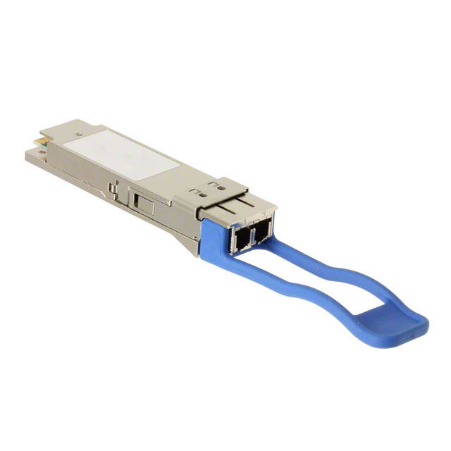
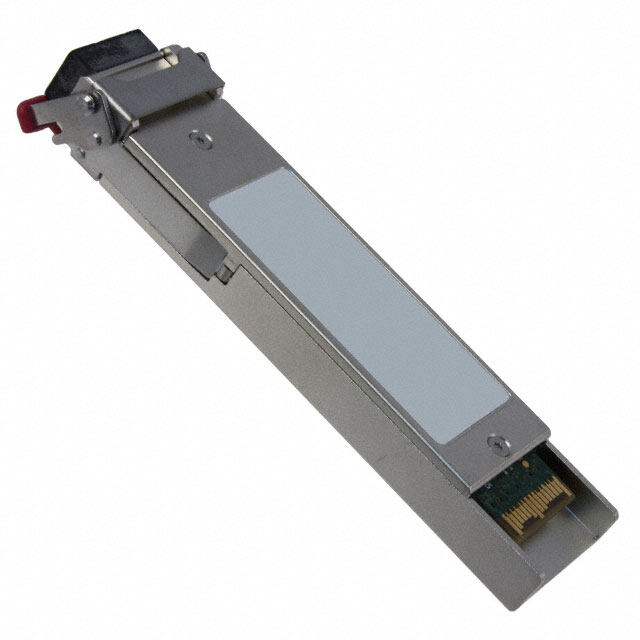
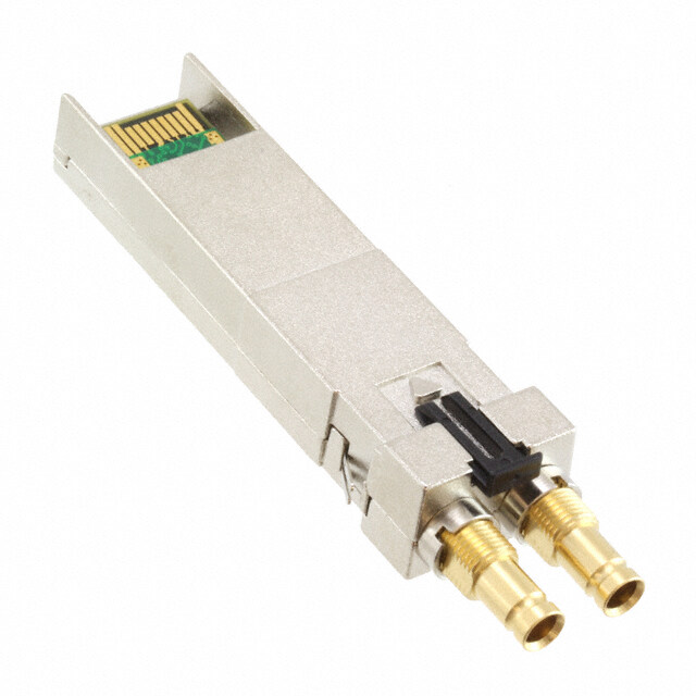
ICGOO电子元器件商城为您提供AFCT-5715APZ由Avago Technologies设计生产,在icgoo商城现货销售,并且可以通过原厂、代理商等渠道进行代购。 AFCT-5715APZ价格参考¥278.36-¥375.05。Avago TechnologiesAFCT-5715APZ封装/规格:光纤 - 收发器模块, Fiber Optic Transceiver Module Ethernet 1.25Gbd 1310nm 3.14V ~ 3.47V LC Duplex Pluggable, SFP。您可以下载AFCT-5715APZ参考资料、Datasheet数据手册功能说明书,资料中有AFCT-5715APZ 详细功能的应用电路图电压和使用方法及教程。
| 参数 | 数值 |
| 产品目录 | |
| 描述 | TXRX OPT SFF PLUGGABLE BAIL DMI光纤发射器、接收器、收发器 Transceiver |
| 产品分类 | 光纤 - 收发器光纤 |
| 品牌 | Avago Technologies US Inc. |
| 产品手册 | http://www.avagotech.com/pages/en/optical_transceivers/ethernet/gigabit_ethernet/afct-5715apz/ |
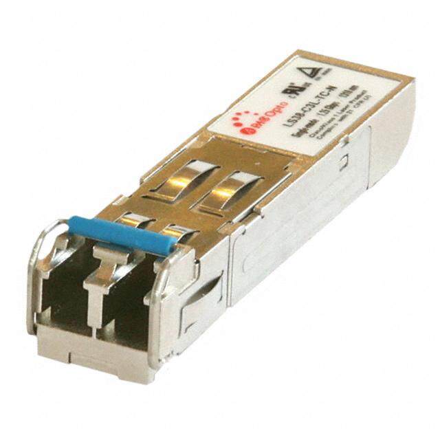
| 产品图片 |
|
| rohs | 符合RoHS无铅 / 符合限制有害物质指令(RoHS)规范要求 |
| 产品系列 | 光纤发射器、接收器、收发器,Avago Technologies AFCT-5715APZ- |
| mouser_ship_limit | 该产品可能需要其他文件才能进口到中国。 |
| 数据手册 | http://www.avagotech.com/docs/AV02-2366EN |
| 产品型号 | AFCT-5715APZ |
| 产品 | Transceivers |
| 产品种类 | 光纤发射器、接收器、收发器 |
| 其它名称 | 516-2590 |
| 商标 | Avago Technologies |
| 安装类型 | 可插入式,SFP |
| 工作电源电压 | 3.3 V |
| 工厂包装数量 | 10 |
| 应用 | 以太网 |
| 数据速率 | 1.25Gbd |
| 最大工作温度 | + 85 C |
| 最小工作温度 | - 40 C |
| 标准包装 | 10 |
| 波长 | 1310nm |
| 电压-电源 | 3.14 V ~ 3.47 V |
| 纤维类型 | Singlemode |
| 连接器类型 | LC 双工 |


- 商务部:美国ITC正式对集成电路等产品启动337调查
- 曝三星4nm工艺存在良率问题 高通将骁龙8 Gen1或转产台积电
- 太阳诱电将投资9.5亿元在常州建新厂生产MLCC 预计2023年完工
- 英特尔发布欧洲新工厂建设计划 深化IDM 2.0 战略
- 台积电先进制程称霸业界 有大客户加持明年业绩稳了
- 达到5530亿美元!SIA预计今年全球半导体销售额将创下新高
- 英特尔拟将自动驾驶子公司Mobileye上市 估值或超500亿美元
- 三星加码芯片和SET,合并消费电子和移动部门,撤换高东真等 CEO
- 三星电子宣布重大人事变动 还合并消费电子和移动部门
- 海关总署:前11个月进口集成电路产品价值2.52万亿元 增长14.8%


PDF Datasheet 数据手册内容提取
AFCT-5710Z and AFCT-5715Z Families of Single-Mode Small Form Factor Pluggable (SFP) Optical Transceivers with Optional DMI for Gigabit Ethernet (1.25 GBd) Data Sheet Description Features The AFCT-571xZ family of Small Form Factor Pluggable • ROHS-6 Compliant (SFP) LC optical transceivers off ers a wide range of • Optional Digital Diagnostic Monitoring available design options, including optional DMI features (further - AFCT-5710Z family: without DMI described later), two temperature ranges (extended or - AFCT-5715Z family: with DMI industrial), and choice of standard or bail delatch. The • Per SFF-8472, diagnostic features on AFCT-5715Z AFCT-5715Z family targets applications requiring DMI, family enable Diagnostic Monitoring Interface for while the AFCT-5710Z family is streamlined for those optical transceivers with real-time monitoring of: applications where DMI is not needed. Throughout this - Transmitted optical power datasheet, AFCT-571xZ will refer to the entire product - Received optical power family encompassing this full range of product options. - Laser bias current - Temperature Part Number Options - Supply voltage The AFCT-571xZ SFP family consists of the following • Compliant to IEEE 802.3Z Gigabit Ethernet (1.25 GBd) products: 1000BASE-LX & Small Form Factor Pluggable (SFP) Part Number DMI Temperature Latch Design Multi-Source Agreement (MSA) AFCT-5710LZ No Extended Standard • Manufactured in an ISO 9001 compliant facility AFCT-5710PZ No Extended Bail • Hot-pluggable AFCT-5710ALZ No Industrial Standard • Temperature options AFCT-5710APZ No Industrial Bail (Extended) -10°C to +85°C AFCT-5715LZ Yes Extended Standard (Industrial) -40°C to +85°C AFCT-5715PZ Yes Extended Bail • +3.3 V dc power supply AFCT-5715ALZ Yes Industrial Standard • 1310 nm longwave laser AFCT-5715APZ Yes Industrial Bail • Eye safety certifi ed: * Extended Temperature Range is -10 to 85 degrees C - US 21 CFR(J) Industrial Temperature Range is -40 to 85 degrees C - IEC 60825-1 (+All) Related Products • LC-Duplex fi ber connector compatible • AFBR-5705Z SFP family: 1.25GBd Ethernet • Link Lengths at 1.25 GBd: (1000BASE-SX) & 1.0625GBd Fiber Channel with DMI - 0.5 to 550 m - 50 μm MMF • AFBR-5701Z SFP family: 1.25GBd Ethernet - 0.5 to 550 m - 62.5 μm MMF - 0.5 m to 10 km - SMF (1000BASE-SX) & 1.0625GBd Fiber Channel without DMI Applications • AFCT-5715Z SFP family: 1.25GBd Ethernet • Ethernet Switch (1000BASE-LX) with DMI • Enterprise Router • AFCT-5710Z SFP family: 1.25GBd Ethernet • Broadband aggregation and wireless infrastructure (1000BASE-LX) without DMI • Metro Ethernet multi-service access & provisioning platforms
Overview SFP MSA Compliance The AFCT-571xZ family is compliant with both IEEE The product package is compliant with the SFP MSA with 802.3Z (1000BASE-LX) and the SFP Multi-Source the LC connector option. The SFP MSA includes specifi ca- Agreement (MSA) specifi cation. These transceivers tions for mechanical packaging and performance as well are intended for premise, public and access network- as dc, ac and control signal timing and performance. ing applications. They are qualifi ed in accordance with The power supply is 3.3 V dc. GR-468-CORE, and transmit data over single-mode (SM) fi ber for a link distance of 10 km, in excess of the The High Speed I/O (HSIO) signal interface is a Low standard. Voltage Diff erential type. It is ac coupled and terminated internally to the module. The internal termination is a The AFCT-5715Z family of optical transceivers adds 100 Ohm diff erential load. digital diagnostic monitoring to standard SFP function- ality, enabling fault isolation, components monitoring Installation and failure prediction capabilities. The AFCT-571xZ can be installed in or removed from General Features any MSA-compliant Pluggable Small Form Factor (SFP) port regardless of whether the host equipment is The AFCT-571xZ is compliant to 1 GbE specifi cations. operating or not. The module is simply inserted, electri- This includes specifi cations for the signal coding, optical cal-interface fi rst, under fi nger-pressure. Controlled hot- fi ber and connector types, optical and electrical trans- plugging is ensured by 3-stage pin sequencing at the mitter characteristics, optical and electrical receiver electrical interface. This printed circuit board card-edge characteristics, jitter characteristics, and compliance connector is depicted in Figure 2. testing methodology for the aforementioned. As the module is inserted, fi rst contact is made by This transceiver is capable of implementing both Single the housing ground shield, discharging any poten- Mode (SM) and Multimode (MM) optical fi ber applica- tially component-damaging static electricity. Ground tions in that order of precedence in the event of con- pins engage next and are followed by Tx and Rx fl icting specifi cations. In addition, the SM link type power supplies. Finally, signal lines are connected. Pin exceeds the 2 m to 5 km 1000BASE-LX specifi cation by functions and sequencing are listed in Table 2. achieving compliance over 2 m to 10 km. The MM link type is expected to meet the 62.5 μm MMF specifi cation when used with an “off set launch” fi ber. Receiver Electrical Interface Optical Interface Amplification RD+ (Receive Data) Light from Fiber Photo-Detector & Quantization RD- (Receive Data) Rx Loss Of Signal MOD-DEF2 (SDA) text Controller & Memory MOD-DEF1 (SCL) MOD-DEF0 Transmitter TX_DISABLE TD+ (Transmit Data) Laser Driver & Light to Fiber Laser Safety Circuit TD- (Transmit Data) TX_FAULT Figure 1. Transceiver Functional Diagram 2
3 2 1 3 2 1 Transmitter Section ENGAGEMENT 20 VEET SEQUENCE 1 VEET The transmitter section includes a 1310 nm Fabry-Perot laser and a transmitter driver circuit. The driver circuit 19 TD– 2 TX FAULT maintains a constant optical power level provided that 18 TD+ 3 TX DISABLE the data pattern is valid 8B/10B code. Connection to the transmitter is provided via a LC optical connector. 17 VEET 4 MOD-DEF(2) The transmitter has full IEC 60825 and CDRH Class 1 eye 16 VCCT 5 MOD-DEF(1) safety. 15 VCCR 6 MOD-DEF(0) TX_DISABLE 14 VEER 7 RATE SELECT The transmitter output can be disabled by asserting pin 13 RD+ 8 LOS 3, TX_DISABLE. A high signal asserts this function while a low signal allows normal laser operation. In addition, 12 RD– 9 VEER via the 2-wire serial interface the transmitter output can 11 VEER 10 VEER be disabled (address A2h, byte 110, bit 6) or monitored (address A2h, byte 110, bit 7). The contents of A2h, byte TOP OF BOARD BOTTOM OF BOARD 110, bit 6 are logic OR’d with hardware Tx_Disable (pin (AS VIEWED THROUGH TOP OF BOARD) 3) to control transmitter operation. In the event of a Figure 2. Pin description of the SFP electrical interface. transceiver fault, such as the activation of the eye safety circuit, toggling of the TX_DISABLE will reset the trans- mitter, as depicted in Figure 4. 1 µH 3.3 V 10 µF 0.1 µF 1 µH 3.3 V VCC,T SFP MODULE 0.1 µF 4.7 K to 10 KΩ 4.7 K to 10 KΩ Tx_DISABLE Tx_FAULT Tx_FAULT 0.01 µF VREFR VREFR SO+ 50Ω TD+ LASER DRIVER TX[0:9] 100 Ω & SAFETY SO– 50Ω TD– CIRCUITRY TBC TBC TX GND 0.01 µF EWRAP EWRAP VCC,R 4.7 K to 10 KΩ VCC,R PROTOICCOL 10 µF 0µ.F1 50 Ω RX[0:9] 0.01 µF 50 Ω RD+ SI+ RBC RBC Rx_RATE Rx_RRAETFECLK SI– 100 Ω 50 Ω RD– AMPLIF&ICATION QUANTIZATION Rx_LOS 0.01 µF Rx_LOS RX GND 50 Ω MOD_DEF2 VCC,R GPIO(X) MOD_DEF1 GPIO(X) EEPROM MOD_DEF0 GP14 REFCLK 4.7 K to 4.7 K to 4.7 K to 10 KΩ 10 KΩ 10 KΩ 106.25 MHz 3.3 V Figure 3. Typical Application Confi guration 3
TX_FAULT Functional Data I/O A laser fault or a low VCC condition will activate the Avago’s AFCT-571xZ transceiver is designed to accept transmitter fault signal, TX_FAULT, and disable the laser. industry standard diff erential signals. The transceiver This signal is an open collector output (pull-up required provides an AC-coupled, internally terminated data on the host board); A low signal indicates normal laser interface. Bias resistors and coupling capacitors have operation and a high signal indicates a fault. The TX_ been included within the module to reduce the number FAULT will be latched high when a laser fault occurs and of components required on the customer’s board. is cleared by toggling the TX_DISABLE input or power Figure 2 illustrates the recommended interface circuit. cycling the transceiver. The TX_FAULT is not latched Digital Diagnostic Interface and Serial Identifi cation for Low VCC. The transmitter fault condition can also be monitored via the two-wire serial interface (address The AFCT-571xZ family complies with the SFF-8074i A2h, byte 110, bit 2). specifi cation, which defi nes the module’s serial identifi - cation protocol to use the 2-wire serial CMOS EEPROM Eye Safety Circuit protocol of the ATMEL AT24C01A or similar. Standard Under normal operating conditions, the laser power SFP EEPROM bytes 0-255 are addressed per SFF-8074i at will be maintained below the eye-safety limit. If the memory address 0xA0 (A0h). eye safety limit is exceeded at any time, a laser fault will As an enhancement to the conventional SFP interface occur and the TX_FAULT output will be activated. defi ned in SFF-8074i, the AFCT-5715Z is also compliant Receiver Section to SFF-8472 (the digital diagnostic interface for SFP). This enhancement adds digital diagnostic monitoring The receiver section for the AFCT-571xZ contains an to standard SFP functionality, enabling failure predic- InGaAs/InP photo detector and a preamplifi er mounted tion, fault isolation, and component monitoring capa- in an optical subassembly. This optical subassembly is bilities. coupled to a post amplifi er/decision circuit on a circuit Using the 2-wire serial interface, the AFCT-5715Z board. The design of the optical subassembly provides provides real time access to transceiver internal supply better than 12 dB Optical Return Loss (ORL). voltage and temperature, transmitter output power, Connection to the receiver is provided via a LC optical laser bias current and receiver average input power, connector. allowing a host to predict system compliance issues. These fi ve parameters are internally calibrated, per the RX_LOS MSA. New digital diagnostic information is accessed The receiver section contains a loss of signal (RX_LOS) per SFF-8472 using EEPROM bytes 0-255 at memory circuit to indicate when the optical input signal power address 0xA2 (A2h). is insuffi cient for Gigabit Ethernet compliance. A high The digital diagnostic interface also adds the ability to signal indicates loss of modulated signal, indicating link disable the transmitter (TX_DISABLE), monitor for Trans- failure such as a broken fi ber or a failed transmitter. RX_ mitter Faults (TX_FAULT) and monitor for Receiver Loss LOS can be also be monitored via the two-wire serial of Signal (RX_LOS). (address A2h, byte 110, bit 1). Contents of the MSA-compliant serial ID memory are 1 µH shown in Tables 10 through 14. The SFF-8074i and VCCT SFF-8472 specifi cations are available from the SFF 0.1 µF Committee at http://www.sff committee.org. 1 µH The I2C accessible memory page address 0xB0 is used V R 3.3 V CC internally by SFP for the test and diagnostic purposes 0.1 µF 10 µF 0.1 µF 10 µF and it is reserved. Predictive Failure Identifi cation SFP MODULE HOST BOARD The diagnostic information allows the host system to identify potential link problems. Once identifi ed, a Figure 4. MSA required power supply fi lter fail-over technique can be used to isolate and replace suspect devices before system uptime is impacted. 4
Compliance Prediction Operating Temperature The real-time diagnostic parameters can be monitored The AFCT-571xZ family is available in either Extended to alert the system when operating limits are exceeded (-10 to +85°C) or Industrial (-40 to +85°C) temperature and compliance cannot be ensured. ranges. Fault Isolation Power Supply Noise The diagnostic information can allow the host to The AFCT-571xZ can withstand an injection of PSN on pinpoint the location of a link problem and accelerate the V lines of 100 mV ac with a degradation in eye CC system servicing and minimize downtime. mask margin of up to 10% on the transmitter and a 1 dB sensitivity penalty on the receiver. This occurs when Component Monitoring the product is used in conjunction with the MSA rec- ommended power supply fi lter shown in Figure 3. As part of the host system monitoring, the real time diagnostic information can be combined with system Regulatory Compliance level monitoring to ensure system reliability. The transceiver regulatory compliance is provided in Application Support Table 1 as a fi gure of merit to assist the designer. The overall equipment design will determine the certifi ca- An Evaluation Kit and Reference Designs are available tion level. to assist in evaluation of the AFCT-571xZ SFPs. Please contact your local Field Sales representative for avail- ability and ordering details. Table 1. Regulatory Compliance Feature Test Method Performance Electrostatic Discharge (ESD) MIL-STD-883C Method 3015.4 Class 2 (>2000 Volts) to the Electrical Pins JEDEC/EIA JESD22-A114-A Electrostatic Discharge (ESD) Bellcore GR1089-CORE 25 kV Air Discharge to the Duplex LC Receptacle 10 Zaps at 8 kV (contact discharge) on the electri- cal faceplate on panel. Electromagnetic Interference FCC Class B Applications with high SFP port counts are ex- (EMI) pected to be compliant; however, margins are de- pendent on customer board and chassis design. Immunity Variation of IEC 61000-4-3 No measurable eff ect from a 10 V/m fi eld swept from 80 to 1000 MHz applied to the transceiver without a chassis enclosure. Eye Safety US FDA CDRH AEL Class 1 CDRH certifi cation # 9521220-132 EN (IEC) 60825-1, 2, TUV fi le R72102126.01 EN60950 Class 1 Component Recognition Underwriter’s Laboratories and UL fi le # E173874 Canadian Standards Association Joint Component Recognition for Informa- tion Technology Equipment Including Electrical Business Equipment ROHS Compliance Less than 1000ppm of: cadmium, lead, mercury, hexavalent chromium, polybrominated biphenyls, and polybrominated biphenyl ethers 5
Electrostatic Discharge (ESD) Eye Safety There are two conditions in which immunity to ESD The AFCT-571xZ transceivers provide Class 1 eye damage is important: safety by design. Avago Technologies has tested the transceiver design for regulatory compliance, under The fi rst condition is static discharge to the transceiver normal operating conditions and under a single fault during handling such as when the transceiver is inserted condition. See Table 1. into the transceiver port. To protect the transceiver, it is important to use normal ESD handling precau- Flammability tions including the use of grounded wrist straps, work benches, and fl oor mats in ESD controlled areas. The ESD The AFCT-571xZ family of SFPs is compliant to UL sensitivity of the AFCT-571xZ is compatible with typical 94V-0. industry production environments. Customer Manufacturing Processes The second condition is static discharge to the exterior This module is pluggable and is not designed for of the host equipment chassis after installation. To the aqueous wash, IR refl ow, or wave soldering processes. extent that the duplex LC optical interface is exposed to the outside of the host equipment chassis, it may be Caution subject to system-level ESD requirements. The ESD per- formance of the AFCT-571xZ exceeds typical industry The AFCT-571xZ contains no user-serviceable parts. standards. Table 1 documents ESD immunity to both of Tampering with or modifying the performance of the these conditions. AFCT-571xZ will result in voided product warranty. It may also result in improper operation of the transceiver Electromagnetic Interference (EMI) circuitry, and possible over-stress of the laser source. Device degradation or product failure may result. Most equipment designs using the AFCT-571xZ SFPs Connection of the AFCT-571xZ to a non-approved are subject to the requirements of the FCC in the optical source, operating above the recommended United States, CENELEC EN55022 (CISPR 22) in Europe absolute maximum conditions may be considered an and VCCI in Japan. The metal housing and shielded act of modifying or manufacturing a laser product. The design of the transceiver minimize EMI and provide person(s) performing such an act is required by law to excellent EMI performance. re-certify and re-identify the laser product under the EMI Immunity provisions of U.S. 21 CF. The AFCT-571xZ transceivers have a shielded design to provide excellent immunity to radio frequency electromagnetic fi elds which may be present in some operating environments. 6
Table 2. Pin description Engagement Pin Name Function/Description Order(insertion) Notes 1 VeeT Transmitter Ground 1 2 TX Fault Transmitter Fault Indication 3 1 3 TX Disable Transmitter Disable - Module disables on high or open 3 2 4 MOD-DEF2 Module Defi nition 2 - Two wire serial ID interface 3 3 5 MOD-DEF1 Module Defi nition 1 - Two wire serial ID interface 3 3 6 MOD-DEF0 Module Defi nition 0 - Grounded in module 3 3 7 Rate Selection Not Connected 3 8 LOS Loss of Signal 3 4 9 VeeR Receiver Ground 1 10 VeeR Receiver Ground 1 11 VeeR Receiver Ground 1 12 RD- Inverse Received Data Out 3 5 13 RD+ Received Data Out 3 5 14 VeeR Reciver Ground 1 15 VccR Receiver Power -3.3 V ±5% 2 6 16 VccT Transmitter Power -3.3 V ±5% 2 6 17 VeeT Transmitter Ground 1 18 TD+ Transmitter Data In 3 7 19 TD- Inverse Transmitter Data In 3 7 20 VeeT Transmitter Ground 1 Notes: 1. TX Fault is an open collector/drain output which should be pulled up externally with a 4.7KΩ – 10 KΩ resistor on the host board to a supply <VccT+0.3 V or VccR+0.3 V. When high, this output indicates a laser fault of some kind. Low indicates normal operation. In the low state, the output will be pulled to < 0.8 V. 2. TX disable input is used to shut down the laser output per the state table below. It is pulled up within the module with a 4.7-10 KΩ resistor. Low (0 – 0.8 V): Transmitter on Between (0.8 V and 2.0 V): Undefi ned High (2.0 – 3.465 V): Transmitter Disabled Open: Transmitter Disabled 3. Mod-Def 0,1,2. These are the module defi nition pins. They should be pulled up with a 4.7-10 KΩ resistor on the host board to a supply less than VccT +0.3 V or VccR+0.3 V. Mod-Def 0 is grounded by the module to indicate that the module is present Mod-Def 1 is clock line of two wire serial interface for optional serial ID Mod-Def 2 is data line of two wire serial interface for optional serial ID 4. LOS (Loss of Signal) is an open collector/drain output which should be pulled up externally with a 4.7 KΩ – 10 KΩ resistor on the host board to a supply < VccT,R+0.3 V. When high, this output indicates the received optical power is below the worst case receiver sensitivity (as defi ned by the standard in use). Low indicates normal operation. In the low state, the output will be pulled to < 0.8 V. 5. RD-/+: These are the diff erential receiver outputs. They are AC coupled 100 Ω diff erential lines which should be terminated with 100 Ω diff erential at the user SERDES. The AC coupling is done inside the module and is thus not required on the host board. The voltage swing on these lines must be between 370 and 2000 mV diff erential (185 – 1000 mV single ended) according to the MSA. Typically it will be 1500mv diff erential. 6. VccR and VccT are the receiver and transmitter power supplies. They are defi ned as 3.135 – 3.465 V at the SFP connector pin. The in-rush current will typically be no more than 30 mA above steady state supply current after 500 nanoseconds. 7. TD-/+: These are the diff erential transmitter inputs. They are AC coupled diff erential lines with 100 Ω diff erential termination inside the module. The AC coupling is done inside the module and is thus not required on the host board. The inputs will accept diff erential swings of 500 – 2400 mV (250 – 1200 mV single ended). However, the applicable recommended diff erential voltage swing is found in Table 5. 7
Table 3. Absolute Maximum Ratings Absolute maximum ratings are those values beyond which functional performance is not intended, device reliabil- ity is not implied, and damage to the device may occur. Parameter Symbol Minimum Maximum Unit Notes Storage Temperature (non-operating) TS -40 +100 ° C Relative Humidity RH 5 95 % Case Temperature TC -40 85 ° C Supply Voltage VCC -0.5 3.8 V 1 Control Input Voltage VI -0.5 VCC+0.5 V Table 4. Recommended Operating Conditions Typical operating conditions are those values for which functional performance and device reliability is implied. Parameter Symbol Minimum Typical Maximum Unit Notes Case Operating Temperature AFCT-5710LZ/PZ & AFCT-5715LZ/PZ TC -10 +85 ° C AFCT-5710ALZ/APZ & AFCT-5715ALZ/APZ TC -40 +85 ° C Supply Voltage VCC 3.14 3.3 3.47 V Table 5. Transceiver Electrical Characteristics Parameter Symbol Minimum Typical Maximum Unit Notes Module supply current ICC 200 240 mA 2 Power Dissipation PDISS 660 830 mW 2 AC Electrical Characteristics Power Supply Noise Rejection (peak - peak) PSNR 100 mV 3 Inrush Current 30 mA DC Electrical Characteristics Sense Outputs: VOH 2.0 VccT, R+0.3 V 4 Transmit Fault (TX_FAULT) Loss of Signal (LOS) MOD-DEF2 VOL 0.8 V Control Inputs: VIH 2.0 Vcc V 4,5 Transmitter Disable (TX_DISABLE) MOD-DEF1, 2 VIL 0.8 V Data Input: VI 500 2400 mV 6 Transmitter Diff erential Input Voltage (TD+/-) Data Ouput: VO 370 1600 mV 7 Receiver Diff erential Output Voltage (RD+/-) Receiver Data Rise and Fall Times Trf 400 ps Receiver Contributed Total Jitter TJ 0.33267 UIps 8 Notes: 1 The module supply voltages, VccT and VccR, must not diff er by more than 0.5V or damage to the device may occur. 2. Over temperature and Beginning of Life. 3. MSA fi lter is required on host board 10 Hz to 1 MHz. See Figure 3 4. LVTTL, External 4.7 - 10 KΩ Pull-Up Resistor required 5. LVTTL, Internal 4.7 - 10 KΩ Pull-Up Resistor required for TX_Disable 6. Internally ac coupled and terminated (100 Ohm diff erential) 7. Internally ac coupled and load termination located at the user SerDes 8. Per IEEE 802.3 8
Table 6. Transmitter Optical Characteristics Parameter Symbol Minimum Typical Maximum Unit Notes Average Optical Output Power POUT -9.5 -3 dBm Note 1 Optical Extinction Ratio ER 9 dB TX Optical Eye Mask Margin MM 0 30 % Note 3 Center Wavelength λC 1270 1355 nm Spectral Width - rms σ, rms nm Optical Rise/Fall Time tr, tf 260 ps 20-80% Relative Intensity Noise RIN -120 dB/Hz Contributed Total Jitter (Transmitter) TJ 0.284 UI Note 2 1.25 Gb/s 227 ps POUT TX_DISABLE Asserted POFF -45 dBm Notes: 1. Class 1 Laser Safety per FDA/CDRH 2. Contributed total jitter is calculated from DJ and RJ measurements using TJ = RJ + DJ. Contributed RJ is calculated for 1x10-12 BER by multiplying the RMS jitter (measured on a single rise or fall edge) from the oscilloscope by 14. Per FC-PI (Table 9 - SM jitter output, note 1), the actual contributed RJ is allowed to increase above its limit if the actual contributed DJ decreases below its limits, as long as the component output DJ and TJ remain within their specifi ed FC-PI maximum limits with the worst case specifi ed component jitter input. 3. Eye shall be measured with respect to the mask of the eye using fi lter defi ned in IEEE 802.3 section 38.6.5 Table 7. Receiver Optical Characteristics Parameter Symbol Minimum Typical Maximum Unit Notes Input Optical Power PIN -3 dBm Receiver Sensitivity PMIN -19 dBm 1, 2 Stressed Receiver Sensitivity -14.4 dBm (Optical Average Input Power) Receiver Electrical 3 dBUpper 1500 MHz Cutoff Frequency Operating Center Wavelength ΛC 1270 1355 nm Return Loss (minimum) 12 dB Loss of Signal - Assert PA -30 dBm 3 Loss of Signal - De-Assert PD -20 dBm 3 Loss of Signal - Hysteresis PD - PA 0.5 dB Notes: 1. BER = 10-12 2. An average power of -20 dBm with an Extinction Ratio of 9 dB is approximately equivalent to an OMA of 15 μW. 3. These average power values are specifi ed with an Extinction Ratio of 9 dB. The loss-of-signal circuitry responds to valid 8B/10B-encoded peak to peak input optical power, not average power. 9
Table 8. Transceiver Timing Characteristics Parameter Symbol Minimum Maximum Unit Notes Hardware TX_DISABLE Assert Time t_off 10 μs Note 1 Hardware TX_DISABLE Negate Time t_on 1 ms Note 2 Time to initialize, including reset of TX_FAULT t_init 300 ms Note 3 Hardware TX_FAULT Assert Time t_fault 100 μs Note 4 Hardware TX_DISABLE to Reset t_reset 10 μs Note 5 Hardware RX_LOS Assert Time t_loss_on 100 μs Note 6 Hardware RX_LOS De-Assert Time t_loss_off 100 μs Note 7 Software TX_DISABLE Assert Time t_off _soft 100 ms Note 8 Software TX_DISABLE Negate Time t_on_soft 100 ms Note 9 Software Tx_FAULT Assert Time t_fault_soft 100 ms Note 10 Software Rx_LOS Assert Time t_loss_on_soft 100 ms Note 11 Software Rx_LOS De-Assert Time t_loss_off _soft 100 ms Note 12 Analog parameter data ready t_data 1000 ms Note 13 Serial bus hardware ready t_serial 300 ms Note 14 Write Cycle Time t_write 10 ms Note 15 Serial ID Clock Rate f_serial_clock 400 kHz Notes: 1. Time from rising edge of TX_DISABLE to when the optical output falls below 10% of nominal. 2. Time from falling edge of TX_DISABLE to when the modulated optical output rises above 90% of nominal. 3. Time from power on or falling edge of Tx_Disable to when the modulated optical output rises above 90% of nominal. 4. From power on or negation of TX_FAULT using TX_DISABLE. 5. Time TX_DISABLE must be held high to reset the laser fault shutdown circuitry. 6. Time from loss of optical signal to Rx_LOS Assertion. 7. Time from valid optical signal to Rx_LOS De-Assertion. 8. Time from two-wire interface assertion of TX_DISABLE (A2h, byte 110, bit 6) to when the optical output falls below 10% of nominal. Measured from falling clock edge after stop bit of write transaction. 9. Time from two-wire interface de-assertion of TX_DISABLE (A2h, byte 110, bit 6) to when the modulated optical output rises above 90% of nominal. 10. Time from fault to two-wire interface TX_FAULT (A2h, byte 110, bit 2) asserted. 11. Time for two-wire interface assertion of Rx_LOS (A2h, byte 110, bit 1) from loss of optical signal. 12. Time for two-wire interface de-assertion of Rx_LOS (A2h, byte 110, bit 1) from presence of valid optical signal. 13. From power on to data ready bit asserted (A2h, byte 110, bit 0). Data ready indicates analog monitoring circuitry is functional. 14. Time from power on until module is ready for data transmission over the serial bus (reads or writes over A0h and A2h). 15. Time from stop bit to completion of a 1-8 byte write command. Table 9. Transceiver Digital Diagnostic Monitor (Real Time Sense) Characteristics Parameter Symbol Min Units Notes Transceiver Internal Temperature Accuracy TINT ± 3.0 °C Valid from TC = -40 °C to +85 °C Transceiver Internal Supply Voltage Accuracy VINT ± 0.1 V Valid over VCC = 3.3 V ± 5% Transmitter Laser DC Bias Current Accuracy IINT ± 10 % Percentage of nominal bias value Transmitted Average Optical Output Power Accuracy PT ± 3.0 dB Valid from 100 μW to 500μW, avg Received Average Optical Input Power Accuracy PR ± 3.0 dB Valid from 10 μW to 500μW avg 10
VCC > 2.97 V VCC > 2.97 V Tx_FAULT Tx_FAULT Tx_DISABLE Tx_DISABLE TRANSMITTED SIGNAL TRANSMITTED SIGNAL t_init t_init t-init: TX DISABLE NEGATED t-init: TX DISABLE ASSERTED VCC > 2.97 V Tx_FAULT Tx_FAULT Tx_DISABLE Tx_DISABLE TRANSMITTED SIGNAL TRANSMITTED SIGNAL t_off t_on t_init INSERTION t-init: TX DISABLE NEGATED, MODULE HOT PLUGGED t-off & t-on: TX DISABLE ASSERTED THEN NEGATED OCCURANCE OF FAULT OCCURANCE OF FAULT Tx_FAULT Tx_FAULT Tx_DISABLE Tx_DISABLE TRANSMITTED SIGNAL TRANSMITTED SIGNAL t_fault t_reset t_init* * CANNOT READ INPUT... t-fault: TX FAULT ASSERTED, TX SIGNAL NOT RECOVERED t-reset: TX DISABLE ASSERTED THEN NEGATED, TX SIGNAL RECOVERED OCCURANCE OF FAULT Tx_FAULT OCCURANCE OPTICAL SIGNAL OF LOSS Tx_DISABLE TRANSMITTED SIGNAL LOS t_fault t_reset t_loss_on t_loss_off * SFP SHALL CLEAR Tx_FAULT IN t_init* t_init IF THE FAILURE IS TRANSIENT t-fault: TX DISABLE ASSERTED THEN NEGATED, t-loss-on & t-loss-off TX SIGNAL NOT RECOVERED Figure 5. Transceiver Timing Diagrams (Module Installed Except Where Noted) 11
Table 10. EEPROM Serial ID Memory Contents - Page A0h Byte # Data Byte # Data Decimal Hex Notes Decimal Hex Notes 0 03 SFP physical device 37 00 Hex Byte of Vendor OUI (note 3) 1 04 SFP function defi ned by serial ID only 38 17 Hex Byte of Vendor OUI (note 3) 2 07 LC optical connector 39 6A Hex Byte of Vendor OUI (note 3) 3 00 40 41 “A” - Vendor Part Number ASCII character 4 00 41 46 “F” - Vendor Part Number ASCII character 5 00 42 43 “C” - Vendor Part Number ASCII character 6 02 1000BASE-LX 43 54 “T” - Vendor Part Number ASCII character 7 00 44 2D “-” - Vendor Part Number ASCII character 8 00 45 35 “5” - Vendor Part Number ASCII character 9 00 46 37 “7” - Vendor Part Number ASCII character 10 00 47 31 “1” - Vendor Part Number ASCII character 11 01 Compatible with 8B/10B encoded data 48 Note 4 12 0C 1200 MBit/sec nominal bit rate 49 Note 4 13 00 50 Note 4 14 0A 51 Note 4 15 64 52 20 “ “ - Vendor Part Number ASCII character 16 37 Note 1 53 20 “ “ - Vendor Part Number ASCII character 17 37 Note 2 54 20 “ “ - Vendor Part Number ASCII character 18 00 55 20 “ “ - Vendor Part Number ASCII character 19 00 56 20 “ “ - Vendor Revision Number ASCII character 20 41 “A” - Vendor Name ASCII character 57 20 “ “ - Vendor Revision Number ASCII character 21 56 “V” - Vendor Name ASCII character 58 20 “ “ - Vendor Revision Number ASCII character 22 41 “A” - Vendor Name ASCII character 59 20 “ “ - Vendor Revision Number ASCII character 23 47 “G” - Vendor Name ASCII character 60 05 Hex Byte of Laser Wavelength (Note 5) 24 4F “O” - Vendor Name ASCII character 61 1E Hex Byte of Laser Wavelength (Note 5) 25 20 “ “ - Vendor Name ASCII character 62 00 26 20 “ “ - Vendor Name ASCII character 63 Checksum for Bytes 0-62 (Note 6) 27 20 “ “ - Vendor Name ASCII character 64 00 28 20 “ “ - Vendor Name ASCII character 65 1A Hardware SFP TX_DISABLE, TX_FAULT & RX_LOS 29 20 “ “ - Vendor Name ASCII character 66 00 30 20 “ “ - Vendor Name ASCII character 67 00 31 20 “ “ - Vendor Name ASCII character 68-83 Vendor Serial Number ASCII characters (Note7) 32 20 “ “ - Vendor Name ASCII character 84-91 Vendor Date Code ASCII characters (Note 8) 33 20 “ “ - Vendor Name ASCII character 92 Note 4 34 20 “ “ - Vendor Name ASCII character 93 Note 4 35 20 “ “ - Vendor Name ASCII character 94 Note 4 36 00 95 Checksum for Bytes 64-94 (Note 6) 96 - 255 00 Notes: 1. Link distance with 50/125 μm cable. 2. Link distance with 62.5/125 μm. 3. The IEEE Organizationally Unique Identifi er (OUI) assigned to Avago Technologies is 00-17-6A (3 bytes hex). 4. See Table 11 on following page for part number extensions and data-fi elds. 5. Laser wavelength is represented in 16 unsigned bits. The hex representation of 1310 (nm) is 051E. 6. Addresses 63 and 95 are checksums calculated (per SFF-8472 and SFF-8074) and stored prior to product shipment. 7. Addresses 68-83 specify the ASCII serial number and will vary on a per unit basis. 8. Addresses 84-91 specify the ASCII date code and will vary on a per date code basis. 12
Table 11. Part Number Extensions and Datafi elds AFCT-5710ALZ AFCT-5710APZ AFCT-5710LZ AFCT-5710PZ Address Hex ASCII Address Hex ASCII Address Hex ASCII Address Hex ASCII 48 30 0 48 30 0 48 30 0 48 30 0 49 41 A 49 41 A 49 4C L 49 50 P 50 4C L 50 50 P 50 5A Z 50 5A Z 51 5A Z 51 5A Z 51 20 51 20 92 0 92 0 92 0 92 0 93 0 93 0 93 0 93 0 94 0 94 0 94 0 94 0 AFCT-5715ALZ AFCT-5715APZ AFCT-5715LZ AFCT-5715PZ Address Hex ASCII Address Hex ASCII Address Hex ASCII Address Hex ASCII 48 35 5 48 35 5 48 35 5 48 35 5 49 41 A 49 41 A 49 4C L 49 50 P 50 4C L 50 50 P 50 5A Z 50 5A Z 51 5A Z 51 5A Z 51 20 51 20 92 68 92 68 92 68 92 68 93 F0 93 F0 93 F0 93 F0 94 1 94 1 94 1 94 1 13
Table 12. EEPROM Serial ID Memory Contents - Address A2h (AFCT-5715Z family only) Byte # Byte # Byte # Decimal Notes Decimal Notes Decimal Notes 0 Temp H Alarm MSB1 26 Tx Pwr L Alarm MSB4 104 Real Time Rx PAV MSB5 1 Temp H Alarm LSB1 27 Tx Pwr L Alarm LSB4 105 Real Time Rx PAV LSB5 2 Temp L Alarm MSB1 28 Tx Pwr H Warning MSB4 106 Reserved 3 Temp L Alarm LSB1 29 Tx Pwr H Warning LSB4 107 Reserved 4 Temp H Warning MSB1 30 Tx Pwr L Warning MSB4 108 Reserved 5 Temp H Warning LSB1 31 Tx Pwr L Warning LSB4 109 Reserved 6 Temp L Warning MSB1 32 Rx Pwr H Alarm MSB5 110 Status/Control - see Table 13 7 Temp L Warning LSB1 33 Rx Pwr H Alarm LSB5 111 Reserved 8 VCC H Alarm MSB2 34 Rx Pwr L Alarm MSB5 112 Flag Bits - see Table 14 9 VCC H Alarm LSB2 35 Rx Pwr L Alarm LSB5 113 Flag Bit - see Table 14 10 VCC L Alarm MSB2 36 Rx Pwr H Warning MSB5 114 Reserved 11 VCC L Alarm LSB2 37 Rx Pwr H Warning LSB5 115 Reserved 12 VCC H Warning MSB2 38 Rx Pwr L Warning MSB5 116 Flag Bits - see Table 14 13 VCC H Warning LSB2 39 Rx Pwr L Warning LSB5 117 Flag Bits - see Table 14 14 VCC L Warning MSB2 40-55 Reserved 118 Reserved 15 VCC L Warning LSB2 56-94 External Calibration Constants6 119 Reserved 16 Tx Bias H Alarm MSB3 95 Checksum for Bytes 0-947 120-122 Reserved 17 Tx Bias H Alarm LSB3 96 Real Time Temperature MSB1 123 18 Tx Bias L Alarm MSB3 97 Real Time Temperature LSB1 124 19 Tx Bias L Alarm LSB3 98 Real Time Vcc MSB2 125 20 Tx Bias H Warning MSB3 99 Real Time Vcc LSB2 126 21 Tx Bias H Warning LSB3 100 Real Time Tx Bias MSB3 127 Reserved8 22 Tx Bias L Warning MSB3 101 Real Time Tx Bias LSB3 128-247 Customer Writable9 23 Tx Bias L Warning LSB3 102 Real Time Tx Power MSB4 248-255 Vendor Specifi c 24 Tx Pwr H Alarm MSB4 103 Real Time Tx Power LSB4 25 Tx Pwr H Alarm LSB4 Notes: 1. Temperature (Temp) is decoded as a 16 bit signed twos compliment integer in increments of 1/256 °C. 2. Supply voltage (VCC) is decoded as a 16 bit unsigned integer in increments of 100 μV. 3. Laser bias current (Tx Bias) is decoded as a 16 bit unsigned integer in increments of 2 μA. 4. Transmitted average optical power (Tx Pwr) is decoded as a 16 bit unsigned integer in increments of 0.1 μW. 5. Received average optical power (Rx Pwr) is decoded as a 16 bit unsigned integer in increments of 0.1 μW. 6. Bytes 55-94 are not intended from use with AFCT-5715xxxx, but have been set to default values per SFF-8472. 7. Bytes 95 is a checksum calculated (per SFF-8472) and stored prior to product shipment. 8. Byte 127 accepts a write but performs no action (reserved legacy byte). 9. Bytes 128-247 are write enabled (customer writable). 14
Table 13. EEPROM Serial ID Memory Contents - Address A2h, Byte 110 (AFCT-5715Z family only) Bit # Status/Control Name Description 7 Tx Disable State Digital state of SFP Tx Disable Input Pin (1 = Tx_ Disable asserted) 6 Soft Tx Disable Read/write bit for changing digital state of SFP Tx_Disable function1 5 Reserved 4 Rx Rate Select State Digital state of SFP Rate Select Input Pin (1 = full bandwidth of 155 Mbit)2 3 Reserved 2 Tx Fault State Digital state of the SFP Tx Fault Output Pin (1 = Tx Fault asserted) 1 Rx LOS State Digital state of the SFP LOS Output Pin (1 = LOS asserted) 0 Data Ready (Bar) Indicates transceiver is powered and real time sense data is ready (0 = Ready) Notes: 1. Bit 6 is logic OR’d with the SFP Tx_Disable input pin 3 ... either asserted will disable the SFP transmitter. 2. AFCT-5715Z does not respond to state changes on Rate Select Input Pin. It is internally hardwired to full bandwidth. Table 14. EEPROM Serial ID Memory Contents - Address A2h, Bytes 112, 113, 116, 117 (AFCT-5715Z family only) Byte Bit # Flag Bit Name Description 7 Temp High Alarm Set when transceiver nternal temperature exceeds high alarm threshold. 6 Temp Low Alarm Set when transceiver internal temperature exceeds alarm threshold. 5 VCC High Alarm Set when transceiver internal supply voltage exceeds high alarm threshold. 4 VCC Low Alarm Set when transceiver internal supply voltage exceeds low alarm threshold. 112 3 Tx Bias High Alarm Set when transceiver laser bias current exceeds high alarm threshold. 2 Tx Bias Low Alarm Set when transceiver laser bias current exceeds low alarm threshold. 1 Tx Power High Alarm Set when transmitted average optical power exceeds high alarm threshold. 0 Tx Power Low Alarm Set when transmitted average optical power exceeds low alarm threshold. 7 Rx Power High Alarm Set when received P_Avg optical power exceeds high alarm threshold. 113 6 Rx Power Low Alarm Set when received P_Avg optical power exceeds low alarm threshold. 0-5 Reserved 7 Temp High Warning Set when transceiver internal temperature exceeds high warning threshold. 6 Temp Low Warning Set when transceiver internal temperature exceeds low warning threshold. 5 VCC High Warning Set when transceiver internal supply voltage exceeds high warning threshold. 4 VCC Low Warning Set when transceiver internal supply voltage exceeds low warning threshold. 116 3 Tx Bias High Warning Set when transceiver laser bias current exceeds high warning threshold. 2 Tx Bias Low Warning Set when transceiver laser bias current exceeds low warning threshold. 1 Tx Power High Warning Set when transmitted average optical power exceeds high warning threshold. 0 Tx Power Low Warning Set when transmitted average optical power exceeds low warning threshold. 7 Rx Power High Warning Set when received P_Avg optical power exceeds high warning threshold. 117 9 Rx Power Low Warning Set when received P_Avg optical power exceeds low warning threshold. 0-5 Reserved 15
AFCT-571xZ 1300 nm LASER PROD 21CFR(J) CLASS 1 COUNTRY OF ORIGIN YYWW XXXXXX 13.8±0.1 13.4±0.1 [0.541±0.004] [0.528±0.004] 2.60 [0.10] 55.2±0.2 DEVICE SHOWN WITH [2.17±0.01] DUST CAP AND BAIL WIRE DELATCH FRONT EDGE OF SFP TRANSCEIVER CAGE 0.7MAX. UNCOMPRESSED 6.25±0.05 [0.028] [0.246±0.002] 13.0±0.2 8.5±0.1 [0.512±0.008] [0.335±0.004] TX RX AREA FOR PROCESS PLUG 6.6 [0.261] 13.50 [0.53] 14.8 MAX. UNCOMPRESSED [0.583] STANDARD DELATCH 12.1±0.2 [0.48±0.01] DIMENSIONS ARE IN MILLIMETERS (INCHES) Figure 6. Drawing of SFP Transceiver 16
X Y 34.5 10 3x 10x∅1.05± 0.01 7.2 7.1 16.25 ∅ 0.1 L X A S 2.5 ∅ 0.85± 0.05 MIN .PITCH 1 ∅ 0.1 S X Y 2.5 PCB B A 1 EDGE 3.68 5.68 PIN 1 20 8.58 2x 1.7 8.48 16.2514.2511.08 9.611.93 REF. 4.8 11 10 SEE DETAIL 1 2.0 9x 0.95 ± 0.05 11x 11x 2.0 ∅ 0.1 L X A S 26.8 5 2 3 10 3x 41.3 42.3 5 3.2 0.9 20x 0.5 ± 0.03 0.06 L A S B S PIN 1 20 LEGEND 10.93 10.53 11.93 1. PADS AND VIAS ARE CHASSIS GROUND 9.6 0.8 TYP. 2. THROUGH HOLES, PLATING OPTIONAL 11 10 3. HATCHED AREA DENOTES COMPONENT AND TRACE KEEPOUT (EXCEPT CHASSIS GROUND) 4 4. AREA DENOTES COMPONENT 2± 0.005 TYP. KEEPOUT (TRACES ALLOWED) 2x 1.55 ± 0.05 0.06 L A S B S ∅ 0.1 L A S B S DETAIL 1 DIMENSIONS ARE IN MILLIMETERS Figure 7. SFP host board mechanical layout 17
1.7±0.9 [.07±.04] 3.5±0.3 [.14±.01] 41.73±0.5 PCB [1.64±.02] AREA BEZEL FOR PROCESS PLUG 15MAX [.59] Tcase REFERENCE POINT CAGE ASSEMBLY 15.25±0.1 [.60±0.004] 10.4±0.1 12.4REF [.41±0.004] [.49] 10REF 1.15REF 9.8MAX [.39] [.05] [.39] BELOW PCB TO PCB 16.25±0.1MIN PITCH [.64±0.004] 0.4±0.1 [.02±0.004] BELOW PCB MSA-SPECIFIED BEZEL DIMENSIONS ARE IN MILLIMETERS [INCHES]. Figure 8. Assembly Drawing 18
Ordering Information Please contact your local fi eld sales engineer or one of Avago Technologies franchised distributors for ordering information. For technical information, please visit Avago Technologies’ web-page at www.avagotech.com or contact one of Avago Technologies’ regional Technical Response Centers. For information related to SFF Committee documenta- tion visit www.sff committee.org. For product information and a complete list of distributors, please go to our web site: www.avagotech.com Avago, Avago Technologies, and the A logo are trademarks of Avago Technologies in the United States and other countries. Data subject to change. Copyright © 2005-2012 Avago Technologies. All rights reserved. Obsoletes AV01-0167EN AV02-2366EN - September 12, 2012