ICGOO在线商城 > 光电元件 > 光纤 - 收发器模块 > AFBR-5921ALZ

 Datasheet下载
- 型号: AFBR-5921ALZ
- 制造商: Avago Technologies
- 库位|库存: xxxx|xxxx
- 要求:
| 数量阶梯 | 香港交货 | 国内含税 |
| +xxxx | $xxxx | ¥xxxx |
查看当月历史价格
查看今年历史价格
AFBR-5921ALZ产品简介:
ICGOO电子元器件商城为您提供AFBR-5921ALZ由Avago Technologies设计生产,在icgoo商城现货销售,并且可以通过原厂、代理商等渠道进行代购。 AFBR-5921ALZ价格参考。Avago TechnologiesAFBR-5921ALZ封装/规格:光纤 - 收发器模块, Fiber Optic Transceiver Module General Purpose 2.125Gbps 850nm 3.3V LC Duplex Through Hole。您可以下载AFBR-5921ALZ参考资料、Datasheet数据手册功能说明书,资料中有AFBR-5921ALZ 详细功能的应用电路图电压和使用方法及教程。
| 参数 | 数值 |
| 产品目录 | |
| 描述 | TXRX SSF 3.3V 2/1GBS PTH 2X5光纤发射器、接收器、收发器 Transceiver |
| 产品分类 | 光纤 - 收发器光纤 |
| 品牌 | Avago Technologies US Inc. |
| 产品手册 | http://www.avagotech.com/pages/en/optical_transceivers/storage/2g_fibre_channel/afbr-5921alz/ |
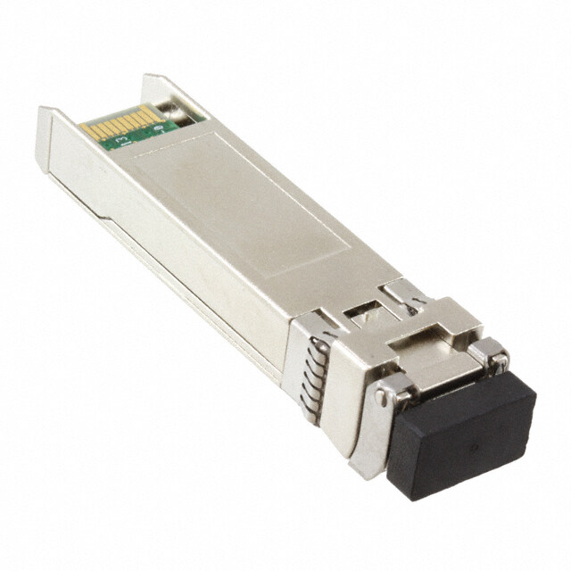
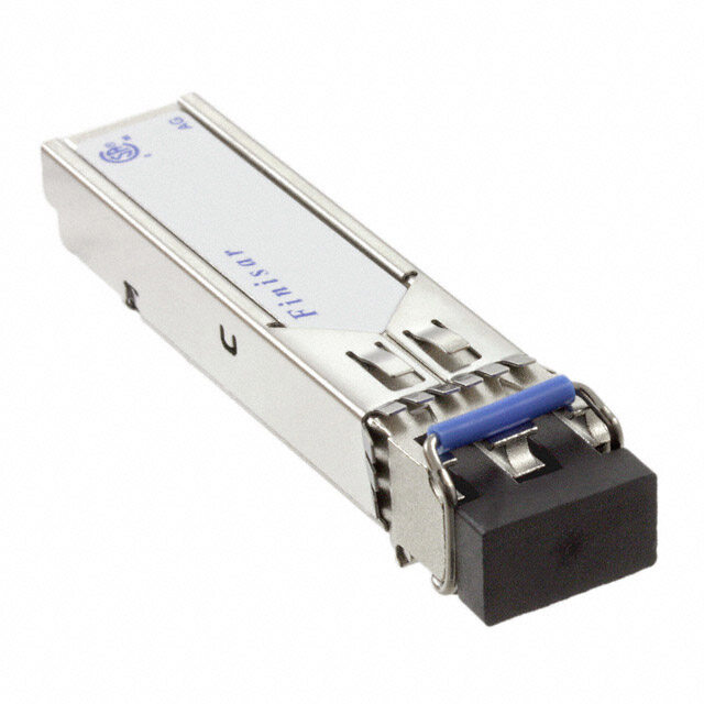
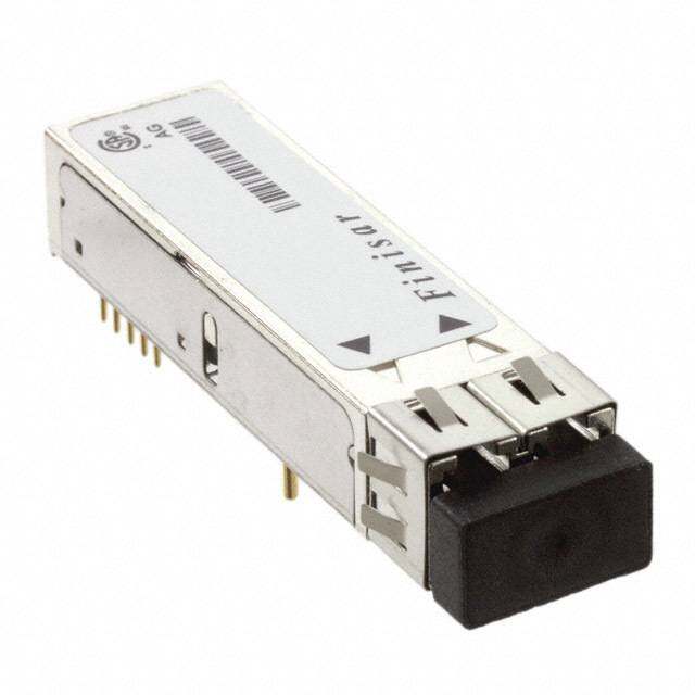
| 产品图片 |
|
| rohs | 符合RoHS无铅 / 符合限制有害物质指令(RoHS)规范要求 |
| 产品系列 | 光纤发射器、接收器、收发器,Avago Technologies AFBR-5921ALZ- |
| mouser_ship_limit | 该产品可能需要其他文件才能进口到中国。 |
| 数据手册 | http://www.avagotech.com/docs/AV02-2199EN |
| 产品型号 | AFBR-5921ALZ |
| 产品 | Transceivers |
| 产品种类 | 光纤发射器、接收器、收发器 |
| 其它名称 | 516-2349 |
| 商标 | Avago Technologies |
| 安装类型 | 通孔 |
| 封装/箱体 | DIP-20 with Connector |
| 工作电源电压 | 3.3 V |
| 工厂包装数量 | 10 |
| 应用 | 通用 |
| 数据速率 | 2.125Gbps |
| 最大工作温度 | + 85 C |
| 最小工作温度 | - 10 C |
| 标准包装 | 10 |
| 波长 | 850nm |
| 电压-电源 | 2.97 V ~ 3.63 V |
| 纤维类型 | Multimode |
| 连接器类型 | LC 双工 |


- 商务部:美国ITC正式对集成电路等产品启动337调查
- 曝三星4nm工艺存在良率问题 高通将骁龙8 Gen1或转产台积电
- 太阳诱电将投资9.5亿元在常州建新厂生产MLCC 预计2023年完工
- 英特尔发布欧洲新工厂建设计划 深化IDM 2.0 战略
- 台积电先进制程称霸业界 有大客户加持明年业绩稳了
- 达到5530亿美元!SIA预计今年全球半导体销售额将创下新高
- 英特尔拟将自动驾驶子公司Mobileye上市 估值或超500亿美元
- 三星加码芯片和SET,合并消费电子和移动部门,撤换高东真等 CEO
- 三星电子宣布重大人事变动 还合并消费电子和移动部门
- 海关总署:前11个月进口集成电路产品价值2.52万亿元 增长14.8%


PDF Datasheet 数据手册内容提取
AFBR-5921ALZ Small Form Factor, Pin Through Hole (PTH), Low Voltage (3.3 V) 2x5 RoHS-Compliant Optical Transceiver for Fibre Channel 2.125/1.0625 GBd 850 nm Data Sheet Description Features The AFBR-5921ALZ from Avago Technologies is a high • Fully RoHS Compliant performance, cost-effective optical transceiver for serial • Datarate specification: 2.125 GBd operation for FC-PI optical data communications applications operating at 200-M5-SN-I and FC-PI 200-M6-SN-I 2.125 Gb/s and 1.0625 Gb/s. This module is designed 1.0625 GBd operation for FC-PI 100-M5-SN-I and FC-PI for multimode fiber and operates at a nominal wave- 100-M6-SN-I length of 850 nm. The transceiver incorporates 3.3 V DC compatible technology including an 850 nm VCSEL • Link lengths at 2.125 GBd: transmitter. The AFBR-5921ALZ offers maximum flex- 0.5 to 300 m – 50/125 µm MMF ibility to Fibre Channel designers, manufacturers, and 0.5 to 150 m – 62.5/125 µm MMF system integrators to implement a range of solutions • Link lengths at 1.0625 GBd: for multi-mode Fibre Channel applications. This product 0.5 to 500 m – 50/125 µm MMF is fully compliant with all equipment meeting the Fibre 0.5 to 300 m – 62.5/125 µm MMF Channel FC-PI 200-M5-SN-I and 200-M6-SN-I 2.125 • Compatible to 2.5G InfiniBand standard GBd specifications, and is compliant with the Fibre Channel FC-PI 100-M5-SN-I, FC-PI 100-M6-SN-I, FC-PH2 • 850 nm Vertical Cavity Surface Emitting Laser (VCSEL) 100-M5-SN- and FC-PH2 100-M6-SN-I 1.0625 GBd • Laser AEL Class I (eye safe) per: specifications. The AFBR-5921ALZ is also suitable for US 21 CFR (J) 2.5Gbps transmission rate InfiniBand applications. The EN 60825-1 (+All) AFBR-5921ALZ is also compatible with the SFF Multi • High Reliability <100 FIT @ 50°C Source Agreement (MSA). • Wide temperature and supply voltage operation Applications • Industry standard 2x5 SFF package • Mass storage system I/O • Wave solder and aqueous wash process compatible • Computer system I/O Related Products • High speed peripheral interface • AFBR-59M5LZ: 850 nm RoHS compliant 2x6 for • High speed switching systems 2.125/1.0625 Gbd for Fibre Channel and 1.25 Gigabit • Host adapter I/O Ethernet • RAID cabinets • InfiniBand network adapters Patent - www.avagotech.com/patents
AFBR-5921ALZ BLOCK DIAGRAM RECEIVER ELECTRICAL INTERFACE RD+ (RECEIVE DATA) AMPLIFICATION LIGHT FROM FIBER PHOTO-DETECTOR & QUANTIZATION RD– (RECEIVE DATA) SIGNAL DETECT OPTICAL INTERFACE TRANSMITTER LASER Tx_DISABLE DRIVER & LIGHT TO FIBER VCSEL TD+ (TRANSMIT DATA) SAFETY CIRCUITRY TD– (TRANSMIT DATA) Figure 1. Transceiver functional diagram. See Table 5 for Process Compatibility Specifications. Module Package PIN DESCRIPTION 6 5 Avago Technologies offers the Pin Through Hole package 7 4 PIN NAME TYPE utilizing an integral LC-Duplex optical interface connector. 8 3 1 Rx GROUND GROUND 9 2 The transceiver uses a reliable 850 nm VCSEL source and 10 1 2 Rx POWER POWER requires a 3.3 V DC power supply for optimal system 3 Rx SD STATUS OUT design. 4 Rx DATA BAR SIGNAL OUT Module Diagrams 5 Rx DATA SIGNAL OUT 6 Tx POWER POWER Figure 1 illustrates the major functional components of the AFBR-5921ALZ. The connection diagram for both modules 7 Tx GROUND GROUND are shown in Figure 2. Figure 6 depicts the external 8 Tx DISABLE CONTROL IN configuration and dimensions of the module. 9 Tx DATA SIGNAL IN 10 Tx DATA BAR SIGNAL IN Installation The AFBR-5921ALZ can be installed in any MSA- compliant Pin Through Hole port. The module Pin Description is shown in Figure 2. TOP VIEW Solder and Wash Process Capability Figure 2. Module pin assignments and pin configuration. These transceivers are delivered with protective process Recommended Solder Fluxes plugs inserted into the LC connector receptacle. This process plug protects the optical subassemblies during Solder fluxes used with the AFBR-5921ALZ should be wave solder and aqueous wash processing and acts as water-soluble, organic fluxes. Recommended solder fluxes a dust cover during shipping. These transceivers are include Lonco 3355-11 from London Chemical West, Inc. compatible with industry standard wave or hand solder of Burbank, CA, and 100 Flux from Alpha-Metals of Jersey processes. City, NJ. 2
Recommended Cleaning/Degreasing Chemicals Functional Data I/O Alcohols: methyl, isopropyl, isobutyl. Avago Technologies’ AFBR-5921ALZ fiber-optic transceiver Aliphatics: hexane, heptane. is designed to accept industry standard differential signals. In order to reduce the number of passive components Other : naphtha. required on the customer’s board, Avago Technologies has Do not use partially halogenated hydrocarbons such as included the functionality of the transmitter bias resistors 1,1.1 trichoroethane or ketones such as MEK, acetone, and coupling capacitors within the fiber optic module. chloroform, ethyl acetate, methylene dichloride, phenol, The transceiver is compatible with an “AC-coupled” con- methylene chloride, or N-methylpyrolldone. Also, Avago figuration and is internally terminated. Figure 1 depicts Technologies does not recommend the use of cleaners the functional diagram of the AFBR-5921ALZ. that use halogenated hydrocarbons because of their Caution should be taken to account for the proper inter- potential environmental harm. connection between the supporting Physical Layer inte- Transmitter Section grated circuits and the AFBR-5921ALZ. Figure 3 illustrates the recommended interface circuit. The transmitter section includes an 850 nm VCSEL (Vertical Cavity Surface Emitting Laser) light source and a transmit- Reference Designs ter driver circuit. The driver circuit maintains a constant Figure 3 depicts a typical application configuration, while optical power level provided that the data pattern is valid Figure 4 depicts the multisourced power supply filter 8B/10B code. Connection to the transmitter is provided circuit design. via an LC optical connector. Regulatory Compliance TX Disable See Table 1 for transceiver Regulatory Compliance perfor- The AFBR-5921ALZ accepts a transmit disable control mance. The overall equipment design will determine the signal input which shuts down the transmitter. A high certification level. The transceiver performance is offered signal implements this function while a low signal allows as a figure of merit to assist the designer. normal laser operation. In the event of a fault (e.g., eye safety circuit activated), cycling this control signal resets Electrostatic Discharge (ESD) the module. The TX Disable control should be actuated upon initialization of the module. See Figure 5 for product There are two conditions in which immunity to ESD timing diagrams. damage is important. Table 1 documents our immunity to both of these conditions. The first condition is during Eye Safety Circuit handling of the transceiver prior to attachment to the PCB. To protect the transceiver, it is important to use normal For an optical transmitter device to be eye-safe in the ESD handling precautions. These precautions include event of a single fault failure, the transmitter will either using grounded wrist straps, work benches, and floor mats maintain normal, eye-safe operation or be disabled. In the in ESD controlled areas. The ESD sensitivity of the AFBR- event of an eye safety fault, the VCSEL will be disabled. 5921ALZ is compatible with typical industry production Receiver Section environments. The second condition is static discharges to the exterior of the host equipment chassis after instal- Connection to the receiver is provided via an LC optical lation. To the extent that the duplex LC optical interface connector. The receiver circuit includes a Signal Detect (SD) is exposed to the outside of the host equipment chassis, circuit which provides an open collector logic low output it may be subject to system-level ESD requirements. The in the absence of a usable input optical signal level. ESD performance of the AFBR-5921ALZ exceeds typical industry standards. Signal Detect Immunity The Signal Detect (SD) output indicates if the optical input signal to the receiver does not meet the minimum Equipment hosting the AFBR-5921ALZ modules will be detectable level for Fibre Channel compliant signals. subjected to radio-frequency electromagnetic fields in When SD is low it indicates loss of signal. When SD is high some environments. The transceivers have good immunity it indicates normal operation. The Signal Detect thresh- to such fields due to their shielded design. olds are set to indicate a definite optical fault has occurred (e.g., disconnected or broken fiber connection to receiver, failed transmitter). 3
Electromagnetic Interference (EMI) Flammability Most equipment designs utilizing these high-speed trans- The AFBR-5921ALZ VCSEL transceiver housing is made ceivers from Avago Technologies will be required to meet of metal and high strength, heat resistant, chemically the requirements of FCC in the United States, CENELEC resistant, and UL 94V-0 flame retardant plastic. EN55022 (CISPR 22) in Europe and VCCI in Japan. The Caution metal housing and shielded design of the AFBR-5921ALZ minimize the EMI challenge facing the host equipment There are no user serviceable parts nor is any mainte- designer. These transceivers provide superior EMI perfor- nance required for the AFBR-5921ALZ. All adjustments are mance. This greatly assists the designer in the manage- made at the factory before shipment to our customers. ment of the overall system EMI performance. Tampering with or modifying the performance of the AFBR-5921ALZ will result in voided product warranty. It Eye Safety may also result in improper operation of the AFBR-5921ALZ These 850 nm VCSEL-based transceivers provide Class 1 circuitry, and possible overstress of the laser source. Device eye safety by design. Avago Technologies has tested the degradation or product failure may result. Connection transceiver design for compliance with the requirements of the AFBR-5921ALZ to a non-approved optical source, listed in Table 1: Regulatory Compliance, under normal operating above the recommended absolute maximum operating conditions and under a single fault condition. conditions or operating the AFBR-5921ALZ in a manner inconsistent with its design and function may result in Reliability hazardous radiation exposure and may be considered an act of modifying or manufacturing a laser product. The These transceivers have an estimated failure rate of <100 person(s) performing such an act is required by law to FITS @ 50°C. re-certify and re-identify the laser product under the provisions of U.S. 21 CFR (Subchapter J) and the TUV. Table 1. Regulatory Compliance Feather Test Method Performance Electrostatic Discharge MIL-STD-889C Method 3015.4 Class 2 (> 2000V) (ESD) to the Electrical Pins Electrostatic Discharge Variation of IEC 61000-4-2 Typically withstand at least 25kV without damage when (ESD) to the Duplex LC the duplex LC connector receptacle is contaced by a Receptacle Human Body Model probe. Electromagnetic Interference FCC Class B CENELEC System margins are dependent on customer board and (EMI) EN55022 Class B (CISPR 22A) chassis design. VCCI Class Immunity Variation of IEC 61000-4-3 Typically shows a negligible effect from a 10 V/m field swept from 80 to 1000 MHz applied to the transceiver without a chassis enclosure. Eye Safety US FDA CDRH AEL Class 1 CDRH file # 9720151-60 EN(IEC)60825-1,2 TUV file #R72102088 EN60950 Class 1 Component Recognition Underwriters Laboratories and UL UL file #TBD Canadian Standards Association Joint Component Recognition for Information Technology Equipment including Electrical Business Equipment. RoHS Compliance Less than 1000 ppm of cadminm, lead, mercury, hexavalent chromium, polybrominated biphenyls and polybrominated biphenyl 4
Ordering Information Please contact your local field sales engineer or one of Avago Technologies franchised distributors for ordering information. For technical information regarding this product, including the MSA, please visit Avago Technologies Semiconductors Products Website at www.avagotech.com. Use the quick search feature to search for this part number. You may also contact Avago Technologies Customer Response Center at 1-800-235-0312. V ,T GND,T CC 6.8 kΩ Tx DIS Tx_DISABLE Tx FAULT Tx_FAULT 0.01 µF TD+ 100 Ω TD- 0.01 µF LASER DRIVER 4.7 to 10 kΩ 1µH V ,T CC 0.1 µF 3.3 V PROTOCOL IC SERDES IC 10 µF 0.1 µF 1µH VCC,R VCC,R V ,R 10 µF 0.1 µF CC 50 Ω 50 Ω 0.01 µF RD+ 100 Ω RD- 0.01 µF RX_SD RX_SD POST AMPLIFIER GND GND Figure 3. Typical application configuration. 1 µH VCCT 0.1 µF 1 µH VCCR 3.3 V 0.1 µF 10 µF 0.1 µF 10 µF SFF MODULE HOST BOARD NOTE: INDUCTORS MUST HAVE LESS THAN 1 Ω SERIES RESISTANCE PER MSA. Figure 4. MSA recommended power supply filter. 5
Table 2. Pin Description Pin Name Function/Descripition MSA Notes 1 VEER Receiver Ground 1 2 VCCR Receiver Power: 3.3V ±10% 5 3 SD Signal Detect 3 4 RD- Inverse Received Data Out 4 5 RD+ Received Data Out 4 6 VCCT Transmitter Power: 3.3V ±10% 5 7 VEET Transmitter Ground 1 8 TX Disable Transmitter Disable: Module disables on High 2 9 TD+ Transmitter Data In 10 TD- Inverse Transmitter Data In Notes: 1. Transmitter an d Receiver Ground are common in the internal module PCB. They are electrically connected to signal ground within the module, and to the housing shield (see Note 5 in Figure 7c). This housing shield is electrically isolated from the nose shield which is connected to chassis ground (see Note 4 in Figure 7c). 2. TX disable input is used to shut down the laser output per the state table below. It is pulled up internally within the module with a 6.8 kW resistor. Low (0 – 0.8 V): Transmitter on Between (0.8 V and 2.0 V): Undefined High (2.0 – 3.63 V): Transmitter Disabled Open: Transmitter Disabled 3 SD (Signal Detect) is a normally high LVTTL output. When high it indicates that the received optical power is adequate for normal operation. When Low, it indicates that the received optical power is below the worst case receiver sensitivity, a fault has occurred, and the link is no longer valid. 4. RD-/+: These are the differential receiver outputs. They are AC coupled 100 ý differential lines which should be terminated with 100 ý differential at the user SerDes. The AC coupling is done inside the module and is thus not required on the host board. The voltage swing on these lines will be between 400 and 2000 mV differential (200 – 1000 mV single ended) when properly terminated. These levels are compatible with CML and LVPECL voltage swings. 5. VCCR and VCCT are the receiver and transmitter power supplies. They are defined as 2.97 – 3.63 V at the PTH connector pin. The maximum supply current is 200 mA. Table 3. Absolute Maximum Ratings Parameter Symbol Minimum Typical Maximum Unit Notes Storage Temperature Ts -40 +100 °C 1 Case Temperature TC -10 +85 °C 1,2 Relative Humidity RH 5 95 % 1 Supply Voltage VCCT,R -0.5 4 V 1,2 Data/Control Input Voltage VI -0.5 VCC + 0.3 V 1 Sense Output Current Signal Detect (SD) ID 5.0 mA 1 Notes: 1. Absolute Maximum Ratings are those values beyond which damage to the device may occur if these limits are exceeded for other than a short period of time. See Reliability Data Sheets for specific reliability performance. 2. Between Absolute Maximum Ratings and the Recommended Operating Conditions, functional performance is not intended, device reliability is not implied, and damage to the device may occur over an extended period of time. 6
Table 4. Recommended Operating Conditions Parameter Symbol Minimum Typical Maximum Unit Notes Case Temperature TC -10 +25 +85 °C 1 Module Supply Voltage VCCT,R 2.97 3.3 3.63 V 1 Data Rate Fibre Channel 1.0625 Gb/s 1 2.125 Note: 1. Recommended operating conditions are those values outside of which functional performance is not intended, device reliability is not implied, and damage to the device may occur over an extended period of time. See Reliability Data Sheet for specific reliability performance. Table 5. Process Compatibility Parameter Symbol Minimum Typical Maximum Unit Notes Hand Lead Solder Temperature Tsolder +260 °C Time ttime 10 see Wave Solder and Aqueous Wash Temperature Tsolder +260 °C 1 Time ttime 10 see 1 Note: 1. Aqueous wash pressure < 110 psi. Table 6. Transceiver Electrical Characteristics (TC = -10°C to +85°C, VCC = 3.3 V ± 10%) Parameter Symbol Minimum Typical Maximum Unit Notes AC Electrical Characteristics Power Supply Noise Rejection(Peak-to-Peak) PSNR 100 mV 1 DC Electrical Characteristics Module Supply Current ICC 200 mA Power Dissipation PDISS 726 mW Sense Outputs:Signal Detect [SD] VOH 24 VCCR+0.3 V 2 VOL 0.4 V Control Inputs: VIH 2.0 VCC + 0.3 V 3 Transmitter Disable [TX_DISABLE] VIL 0.0 0.8 V Notes: 1. MSA filter is required on host board 10 Hz to 2 MHz. 2. LVTTL, 1.2 kW internal pull-up resistor to VCCR. 3. 9.0 KW internal pull-down resistor to VEE. 4. Please refer to the AFBR-5921ALZ Characterization Report for typical values. 7
Table 7. Transmitter and Receiver Electrical Characteristics (TC = -10°C to +85°C, VCC = 3.3 V ± 10%) Parameter Symbol Minimum Typical Maximum Unit Notes Data Input: VI 400 2400 mV 1 Transmitter Differential Input Voltage (TD +/–) Data Output: VO 500 625 2000 mV 2 Receiver Differential Output Voltage (RD +/–) Receive Data Rise and Fall Trise/fall 200 ps 3 Times (Receiver) Contributed Deterministic Jitter DJ 0.1 UI 4,6 (Receiver) 2.125 Gb/s 47 ps Contributed Deterministic Jitter DJ 0.12 UI 4,6 (Receiver) 1.0625 Gb/s 113 ps Contributed Random Jitter RJ 0.162 UI 5,6 (Receiver) 2.125 Gb/s 76 ps Contributed Random Jitter RJ 0.09 UI 5,6 (Receiver) 1.0625 Gb/s 92 ps Notes: 1. Internally AC coupled and terminated (100 Ohm differential). These levels are compatible with CML and LVPECL voltage swings. 2. Internally AC coupled with internal 50 ohm pullups to VCC (single-ended) and a required external 100 ohm differential load termination. 3. 20%-80% Rise and Fall times measured with a 500 MHz signal utilizing a 1010 data pattern. 4. Contributed DJ is measured on an oscilloscope in average mode with 50% threshold and K28.5 pattern. 5. Contributed RJ is calculated for 1E-12 BER by multiplying the RMS jitter (measured on a single rise or fall edge) from the oscilloscope by 14. Per the FC-PI standard (Table 13 - MM jitter output, note 1), the actual contributed RJ is allowed to increase above its limit if the actual contributed DJ decreases below its limits, as long as the component output DJ and TJ remain within their specified FC-PI maximum limits with the worst case specified component jitter input. 6. In a network link, each component’s output jitter equals each component’s input jitter combined with each component’s contributed jitter. Contributed DJ adds in a linear fashion and contributed RJ adds in a RMS fashion. In the Fibre Channel specification, there is a table specifying the input and output DJ and TJ for the receiver at each data rate. In that table, RJ is found from TJ –DJ, where the RX input jitter is noted as Gamma R, and the RX output jitter is noted as Delta R. The AFBR-5921ALZ contributed jitter is such that, if the maximum specified input jitter is present, and is combined with our maximum contributed jitter, then we meet the specified maximum output jitter limits listed in the FC-PI MM jitter specification table. 7. Please refer to the AFBR-5921ALZ Characterization Report for typical values. 8
Table 8. Transmitter Optical Characteristics (TC = -10°C to +85°C, VCC = 3.3 V ± 10%) Parameter Symbol Minimum Typical Maximum Unit Notes Output Optical Power (Average) POUT -10 0 dBm 50/125 µm NA = 0.2 Note 1 POUT -10 0 dBm 62.5/125 µm NA = 0.275 Note 1 Optical Extinction Ratio FR 9 dB Optical Modulation Amplitude OMA 196 uW FC-PI Std (Peak-to-Peak) 2.125 Gb/s Note 2 Optical Modulation Amplitude OMA 156 uW FC-PI Std (Peak-to-Peak) 1.0625 Gb/s Note 3 Center Wavelength lC 830 860 nm FC-PI Std Spectal Width – rms s 0.85 nm FC-PI Std Optical Rise /Fall Time Trise/fall 150 ps 20%–80%, FC-PI Std RIN12(OMA),maximum RIN -117 dB/Hz FC-PI Std Contributed Deterministic Jitter DJ 0.12 UI 4,5 (Transmitter) 2.125 Gb/s 56 ps Contributed Deterministic Jitter DJ 0.09 UI 4,6 (Transmitter) 1.0625 Gb/s 85 ps Contributed Random Jitter RJ 0.134 UI 5,6 (Transmitter) 2.125 Gb/s 63 ps Contributed Random Jitter RJ 0.177 UI 5,6 (Transmitter) 1.0625 Gb/s 167 ps POUTTX_DISABLEAsserted POFF -35 dBm Notes: 1. Max Pout is the lesser of 0 dBm or Maximum allowable per Eye Safety Standard. 2. An OMA of 196 is approximately equal to an average power of –9 dBm assuming an Extinction Ratio of 9 dB. 3. An OMA of 156 is approximately equal to an average power of –10 dBm assuming an Extinction Ratio of 9 dB. 4. Contributed RJ is calculated for 1E-12 BER by multiplying the RMS jitter (measured on a single rise or fall edge) from the oscilloscope by 14. Per the FC-PI standard (Table 13 - MM jitter output, note 1), the actual contributed RJ is allowed to increase above its limit if the actual contributed DJ decreases below its limits, as long as the component output DJ and TJ remain within their specified FC-PI maximum limits with the worst case specified component jitter input. 5. In a network link, each component’s output jitter equals each component’s input jitter combined with each components contributed jitter. Contributed DJ adds in a linear fashion and contributed RJ adds in a RMS fashion. In the Fibre Channel specification, there is a table specifying the input and output DJ and TJ for the transmitter at each data rate. In that table, RJ is found from TJ-DJ, where the TX input jitter is noted as Delta T, and the TX output jitter is noted as Gamma T. The AFBR-5921ALZ contributed jitter is such that, if the maximum specified input jitter is present, and is combined with our maximum contributed jitter, then we meet the specified maximum output jitter limits listed in the FC-PI MM jitter specification table. 6. Please refer to the AFBR-5921ALZ Characterization Report for typical values. 9
Table 9. Receiver Optical Characteristics (TC = -10°C to +85°C, VCC = 3.3 V ± 10%) Parameter Symbol Minimum Typical Maximum Unit Notes Optical Power PIN 0 dBm FC-PI Std Min Optical ModulationAmplitude OMA 49 µW FC-PI Std (Peak-to-Peak) 2.125 Gb/s Note 1 Min Optical ModulationAmplitude OMA 31 µW FC-PI Std (Peak-to-Peak) 1.0625 Gb/s Note 2 Stressed Receiver Sensitivity 62.5µm fiber 2.125 Gb/s OMA 109 µW Note 3 1.0625 Gb/s OMA 67 µW Note 5 50 µm fiber 2.125 Gb/s OMA 96 µW Note 4 1.0625 Gb/s OMA 55 µW Note 5 Return Loss 12 dB FC-PI Std Signal Detect – De-Assert PD -31 -17.5 dBm Signal Detect – Assert PA -17.0 dBm Signal Detect – Hysteresis PA-PD 0.5 3.1 5 dB Notes: 1. An OMA of 49 uW is approximately equal to an average power of -15dBm, and the OMA typical of 16 uW is approximately equal to an average power of -20 dBm, assuming an Extinction Ratio of 9dB. Sensitivity measurements are made at eye center with BER = 1E-10. 2. An OMA of 31 is approximately equal to an average power of –17 dBm assuming an Extinction Ratio of 9 dB. 3. 2.125 Gb/s Stressed receiver vertical eye closure penalty (ISI) min. is 1.26 dB for 50 µm fiber and 2.03 dB for 62.5 µm fiber. Stressed receiver DCD component min. (at TX) is 40 ps. 4. 1.0625 Gb/s Stressed receiver vertical eye closure penalty (ISI) min. is 0.96 dB for 50 µm fiber and 2.18 dB for 62.5 µm fiber. Stressed receiver DCD component min. (at TX) is 80 ps. 5. These average power values are specified with an Extinction Ratio of 9 dB. The Signal Detect circuitry responds to OMA (peak-to-peak) power, not to average power. 6. Please refer to the AFBR-5921ALZ Characterization Report for typical values. Table 10. Transceiver Timing Characteristics (TC = -10°C to +85°C, VCC = 3.3 V ± 10%) Parameter Symbol Minimum Maximum Unit Notes TX Disable Assert Time t_off 10 µs 1 TX Disable Negate Time t_on 1 ms 2 Time to Initialize t_init 30 ms 3 TX Disable to Reset t_reset 10 µs 4 SD Assert Time t_loss_on 100 µs 5 SD De-assert Time t_loss_off 100 µs 6 Notes: 1. Time from rising edge of TX Disable to when the optical output falls below 10% of nominal. 2. Time from falling edge of TX Disable to when the modulated optical output rises above 90% of nominal. 3. From power on or negation of TX Fault using TX Disable. 4. Time TX Disable must be held high to reset TX Fault. 5. Time from optical signal loss to SD Assert. See transceiver timing diagrams. 6. Time from optical signal recovery to SD De-assert. See transceiver timing diagrams. 10
VCC > 2.97 V VCC > 2.97 V Tx_FAULT Tx_FAULT Tx_DISABLE Tx_DISABLE TRANSMITTED SIGNAL TRANSMITTED SIGNAL t_init t_init t-init: TX DISABLE DE-ASSERTED t-init: TX DISABLE ASSERTED Tx_FAULT Tx_DISABLE TRANSMITTED SIGNAL t_off t_on t-off & t-on: TX DISABLE ASSERTED THEN NEGATED OCCURANCE OF FAULT Tx_FAULT Tx_DISABLE TRANSMITTED SIGNAL t_reset * SFP SHALL CLEAR TX_FAULT IN t_init* < t_init IF THE FAILURE IS TRANSIENT t-reset: TX DISABLE ASSERTED THEN NEGATED, TX SIGNAL RECOVERED OCCURANCE OPTICAL SIGNAL OF LOSS Rx_SD t_loss_on t_loss_off t-loss-on & t-loss-off Figure 5. Transceiver timing diagrams. 11
AVAGO AFBR-5921ALZ 17.8 4X Figure 6a. Module drawing. 12
∅ 0.00 M A 2.29 2x ∅ MAX. (AREA FOR EYELETS) 20x Æ 0.81 ± 0.10 (0.090) (0.032 ± 0.004) 25.75 (1.014) SEE NOTE 3 2x ∅ 1 . 4 0 ± 0 .1 0 (NOTE 4) ∅ 0.00 M A (0.055 ± 0.004) 3.00 4x ∅ 1.40 ± 0.10 (NOTE 5) ∅ 0.00 M A (0.118) (0.055 ± 0.004) SEE DETAIL A 3.00 (0.118) 6.00 13.34 12.16 (0.236) (0.525) (0.479) 15.24 MINIMUM PITCH (0.600) DETAIL A (3x) 54321 7.59 10.16 678910 (0.299) (0.400) 1.80 (0.071) SEE DETAIL B 4.57 (0.180) 3.56 7.11 (0.280) (0.140) 1.00 8.89 (0.350) (0.039) 9x 1.78 (0.070) DETAIL B (4x) Notes: 1. This page describes the recommended circuit board layout and front panel openings for SFF transceivers. 2. The hatched areas are keep-out areas reserved for housing standoffs. No metal traces allowed in keep-out areas. 3. This drawing shows extra pin holes for 2x10 pin transceivers. These extra holes are not required for HFBR-5921AL. 4. Holes for mounting studs must be tied to chassis ground. 5. Holes for housing leads must be tied to signal ground. 6. Dimensions are in millimeters (inches). Figure 6b. Recommended SFF host board and front panel layout. For product information and a complete list of distributors, please go to our web site: www.avagotech.com Avago, Avago Technologies, and the A logo are trademarks of Avago Technologies in the United States and other countries. Data subject to change. Copyright © 2005-2012 Avago Technologies. All rights reserved. AV02-2199EN - February 24, 2012