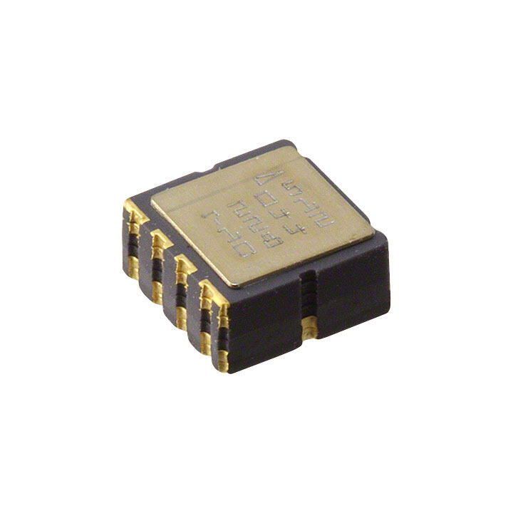
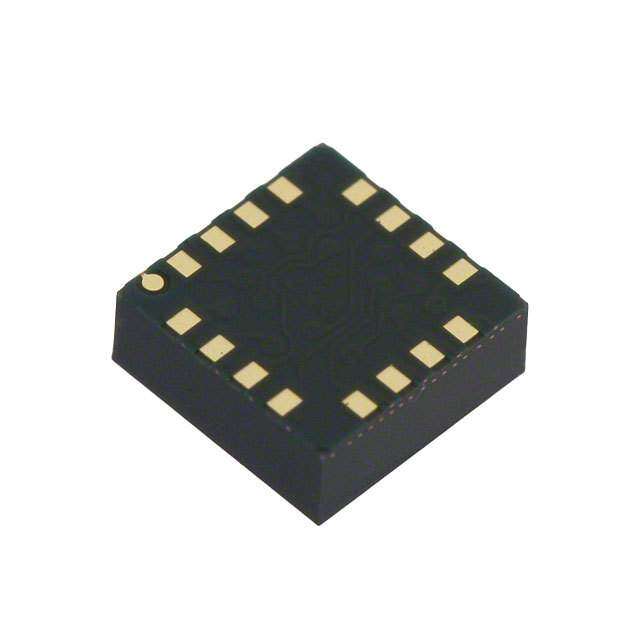
ICGOO在线商城 > 传感器,变送器 > 运动传感器 - 加速计 > ADXL375BCCZ
- 型号: ADXL375BCCZ
- 制造商: Analog
- 库位|库存: xxxx|xxxx
- 要求:
| 数量阶梯 | 香港交货 | 国内含税 |
| +xxxx | $xxxx | ¥xxxx |
查看当月历史价格
查看今年历史价格
ADXL375BCCZ产品简介:
ICGOO电子元器件商城为您提供ADXL375BCCZ由Analog设计生产,在icgoo商城现货销售,并且可以通过原厂、代理商等渠道进行代购。 ADXL375BCCZ价格参考。AnalogADXL375BCCZ封装/规格:运动传感器 - 加速计, Accelerometer X, Y, Z Axis ±200g 0.05Hz ~ 1.6kHz 14-LGA (3x5)。您可以下载ADXL375BCCZ参考资料、Datasheet数据手册功能说明书,资料中有ADXL375BCCZ 详细功能的应用电路图电压和使用方法及教程。
ADXL375BCCZ 是由 Analog Devices Inc. 生产的一款三轴加速度传感器,专为高 g 值冲击和振动检测应用设计。它具有宽测量范围(±200 g)、低噪声、低功耗以及出色的温度稳定性,使其适用于多种工业和消费类应用场景。

 应用场景:

1. 工业设备监控:
   ADXL375BCCZ 可用于监测旋转机械、压缩机、泵等工业设备的振动情况。通过实时检测设备的振动频率和幅度,可以提前发现潜在故障,如轴承磨损或不平衡问题,从而实现预测性维护,减少停机时间和维修成本。

2. 车辆安全与碰撞检测:
   在汽车和摩托车的安全系统中,ADXL375BCCZ 可用于检测碰撞事件。其高 g 值测量范围能够准确捕捉到车辆在高速行驶时发生的剧烈撞击,触发安全气囊展开或其他紧急响应机制,保障乘员安全。

3. 无人机与飞行器控制:
   该传感器可用于无人机的姿态控制和稳定系统。通过精确测量飞行过程中的加速度变化,帮助无人机保持稳定的飞行姿态,避免因外界干扰导致的失控或坠毁。

4. 运动与健身设备:
   在智能穿戴设备和运动器材中,ADXL375BCCZ 可以记录用户的运动状态,如跑步、跳跃等活动中的加速度数据,分析运动强度和姿势,提供个性化的训练建议。

5. 地震监测与结构健康监测:
   该传感器还可应用于地震监测站和建筑物结构健康监测系统中,检测地震波引起的地面振动及建筑物结构的动态响应,评估建筑安全性并预警可能的风险。

6. 物流与运输监控:
   在物流行业中,ADXL375BCCZ 可安装于货物运输车辆或包装箱内,实时监控运输过程中的冲击和振动情况,确保贵重物品的安全运输,防止因不当操作造成的损坏。

总之,ADXL375BCCZ 凭借其高性能和可靠性,在多个领域有着广泛的应用前景。
| 参数 | 数值 |
| 产品目录 | |
| 描述 | IC ACCEL SPI/I2C 3AX 14LGA加速计 Digital Output Three Axis Accel |
| 产品分类 | 加速计运动与定位传感器 |
| 品牌 | Analog Devices Inc |
| 产品手册 | |
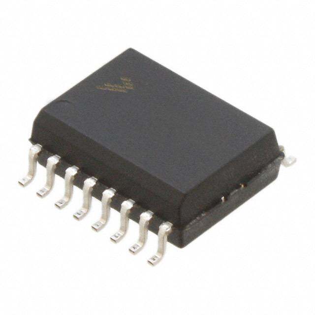
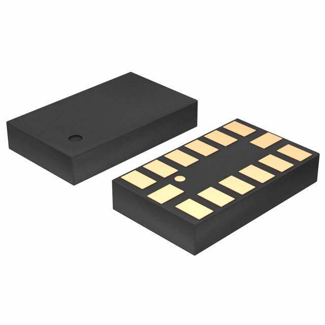
| 产品图片 |
|
| rohs | 符合RoHS无铅 / 符合限制有害物质指令(RoHS)规范要求 |
| 产品系列 | 加速计,Analog Devices ADXL375BCCZ- |
| 数据手册 | |
| 产品型号 | ADXL375BCCZ |
| 产品种类 | 加速计 |
| 传感轴 | Triple |
| 供应商器件封装 | 14-LGA(3x5) |
| 分辨率 | 16 bit |
| 加速 | 2 g, 4 g, 8 g |
| 加速度范围 | ±200g |
| 商标 | Analog Devices |
| 安装类型 | 表面贴装 |
| 安装风格 | SMD/SMT |
| 封装 | Tray |
| 封装/外壳 | 14-VFLGA |
| 封装/箱体 | LGA-14 |
| 工厂包装数量 | 490 |
| 带宽 | 1kHz |
| 接口 | I²C, SPI |
| 数字输出-位数 | 16 bit |
| 数字输出-总线接口 | I2C, SPI |
| 最大工作温度 | + 85 C |
| 最小工作温度 | - 40 C |
| 标准包装 | 1 |
| 灵敏度 | 20.5 LSB/g |
| 电压-电源 | 2 V ~ 3.6 V |
| 电源电压-最大 | 3.6 V |
| 电源电压-最小 | 2 V |
| 电源电流 | 145 uA |
| 轴 | X,Y,Z |
| 输出类型 | I²C, SPI |



- 商务部:美国ITC正式对集成电路等产品启动337调查
- 曝三星4nm工艺存在良率问题 高通将骁龙8 Gen1或转产台积电
- 太阳诱电将投资9.5亿元在常州建新厂生产MLCC 预计2023年完工
- 英特尔发布欧洲新工厂建设计划 深化IDM 2.0 战略
- 台积电先进制程称霸业界 有大客户加持明年业绩稳了
- 达到5530亿美元!SIA预计今年全球半导体销售额将创下新高
- 英特尔拟将自动驾驶子公司Mobileye上市 估值或超500亿美元
- 三星加码芯片和SET,合并消费电子和移动部门,撤换高东真等 CEO
- 三星电子宣布重大人事变动 还合并消费电子和移动部门
- 海关总署:前11个月进口集成电路产品价值2.52万亿元 增长14.8%



PDF Datasheet 数据手册内容提取
REVISIONS LTR DESCRIPTION DATE APPROVED Prepared in accordance with ASME Y14.24 Vendor item drawing REV PAGE REV PAGE REV REV STATUS OF PAGES PAGE 1 2 3 4 5 6 7 8 9 10 PMIC N/A PREPARED BY DLA LAND AND MARITIME COLUMBUS, OHIO 43218-3990 Phu H. Nguyen http://www.landandmaritime.dla.mil/ Original date of drawing CHECKED BY TITLE YY MM DD Phu H. Nguyen MICROCIRCUIT, DIGITAL, 3-AXIS, ±200 g, DIGITAL MEMS ACCELEROMETER, MONOLITHIC SILICON 18-08-09 APPROVED BY Thomas M. Hess SIZE CODE IDENT. NO. DWG NO. A 16236 V62/18612 REV PAGE 1 OF 10 DISTRIBUTION STATEMENT A. Approved for public release. Distribution is unlimited. AMSC N/A 5962-V100-18
1. SCOPE 1.1 Scope. This drawing documents the general requirements of a high performance 3-Axis, ±200 g Digital MEMS Accelerometer microcircuit, with an operating temperature range of -55°C to +105°C. 1.2 Vendor Item Drawing Administrative Control Number. The manufacturer’s PIN is the item of identification. The vendor item drawing establishes an administrative control number for identifying the item on the engineering documentation: V62/18612 - 01 X E Drawing Device type Case outline Lead finish number (See 1.2.1) (See 1.2.2) (See 1.2.3) 1.2.1 Device type(s). Device type Generic Circuit function 01 ADXL375 –EP 3-Axis, ±200 g Digital MEMS Accelerometer 1.2.2 Case outline(s). The case outlines are as specified herein. Outline letter Number of pins Package style X 14 Land Grid Array (LGA) Package 1.2.3 Lead finishes. The lead finishes are as specified below or other lead finishes as provided by the device manufacturer: Finish designator Material A Hot solder dip B Tin-lead plate C Gold plate D Palladium E Gold flash palladium F Tin-lead alloy (BGA/CGA) Z Other SIZE CODE IDENT NO. DWG NO. DLA LAND AND MARITIME COLUMBUS, OHIO A 16236 V62/18612 REV PAGE 2
1.3 Absolute maximum ratings. 1/ Acceleration, Any Axis : Unpowered ....................................................................................... 10000 g Powered ........................................................................................... 10000 g VS ............................................................................................................ -0.3 V to 3.9 V VDD I/O ...................................................................................................... -0.3 V to 3.9 V Digital Pins .............................................................................................. -0.3 V to VDD I/O + 0.3 V or 3.9 V whichever is less Output Short-Circuit Duration (Any Pin to Ground) ................................. Indedfinite Temperature Range: Powered ........................................................................................... -55°C to 105°C Storage ............................................................................................ -65°C to 150°C 1.4 Thermal characteristics. Thermal resistance Case outline θJA θJC Unit Case X 2/ 150 85 °C/W 2. APPLICABLE DOCUMENTS JEDEC – SOLID STATE TECHNOLOGY ASSOCIATION (JEDEC) JESD51 – Methodology for the Thermal Measurement of Component Packages (Single Semiconductor Device). (Applications for copies should be addressed to the Electronic Industries Alliance, 3103 North 10th Street, Suite 240–S, Arlington, VA 22201-2107 or online at https://www.jedec.org) 1/ Stresses beyond those listed under “absolute maximum ratings” may cause permanent damage to the device. These are stress ratings only, and functional operation of the device at these or any other conditions beyond those indicated under “recommended operating conditions” is not implied. Exposure to absolute maximum rated conditions for extended periods may affect device reliability. 2/ Thermal impedance simulated values are based on JEDEC 2S2P thermal test board. See JEDEC JESD-51 SIZE CODE IDENT NO. DWG NO. DLA LAND AND MARITIME COLUMBUS, OHIO A 16236 V62/18612 REV PAGE 3
3. REQUIREMENTS 3.1 Marking. Parts shall be permanently and legibly marked with the manufacturer’s part number as shown in 6.3 herein and as follows: A. Manufacturer’s name, CAGE code, or logo B. Pin 1 identifier C. ESDS identification (optional) 3.2 Unit container. The unit container shall be marked with the manufacturer’s part number and with items A and C (if applicable) above. 3.3 Electrical characteristics. The maximum and recommended operating conditions and electrical performance characteristics are as specified in 1.3, 1.4, and table I herein. 3.4 Design, construction, and physical dimension. The design, construction, and physical dimensions are as specified herein. 3.5 Diagrams. 3.5.1 Case outline. The case outline shall be as shown in 1.2.2 and figure 1. 3.5.2 Terminal connections. The terminal connections shall be as shown in figure 2. 3.5.3 Terminal function. The terminal function shall be as shown in figure 3. 3.5.4 Functional block diagram. The functional block diagram shall be as shown in figure 4. SIZE CODE IDENT NO. DWG NO. DLA LAND AND MARITIME COLUMBUS, OHIO A 16236 V62/18612 REV PAGE 4
TABLE I. Electrical performance characteristics. 1/ Test Test conditions Limits Unit 2/ Min Typ 3/ Max SENSOR INPUT (Each Axis) Measurement Range 4/ ±180 ±200 g Nonlinearity Percentage of full scale ±0.25 % Cross-Axis Sensitivity 5/ ±2.5 % SENSITIVITY (Each Axis) Sensitivity at XOUT, YOUT, ZOUT 4/ 6/ ODR ≤ 800 Hz 18.4 20.5 22.6 LSB/g Scale Factor at XOUT, YOUT, ZOUT 4/ 6/ ODR ≤ 800 Hz 44 49 54 mg/LSB Sensitivity Change Due to Temperature ±0.02 %/°C 0 g OFFSET (Each Axis) 0 g Output for XOUT, YOUT, ZOUT -6000 ±400 +6000 mg 0 g Offset vs. Temperature ±10 mg/°C NOISE Noise X-, y-, and z-axes 5 mg/√Hz OUTPUT DATA RATE AND BANDWIDTH (User selectable) 7/ Output Data Rate (ODR) 6/ 8/ 0.1 3200 Hz SELF-TEST Output Change in Z-Axis 6.4 g POWER SUPPLY Operating Voltage Range (VS) 2.0 2.5 3.6 V Interface Voltage Range (VDD I/O) 1.7 1.8 VS V Supply Current Measurement Mode ODR ≥ 100 Hz 145 µA ODR ≤ 3 Hz 35 µA Standby Mode 0.1 µA Turn-On and Wake-Up Time 10/ ODR = 3200 Hz 1.4 ms TEMPERATURE Operating Temperature Range -55 +105 °C WEIGHT Device Weight 30 mg See footnote at end of table. SIZE CODE IDENT NO. DWG NO. DLA LAND AND MARITIME COLUMBUS, OHIO A 16236 V62/18612 REV PAGE 5
TABLE I. Electrical performance characteristics - Continued. 1/ 1/ Testing and other quality control techniques are used to the extent deemed necessary to assure product performance over the specified temperature range. Product may not necessarily be tested across the full temperature range and all parameters may not necessarily be tested. In the absence of specific parametric testing, product performance is assured by characterization and/or design. 2/ TA = 25°C, VS = 2.5 V, VDD I/O = 2.5 V, acceleration = 0 g, CS = 10 μF tantalum, CI/O = 0.1 μF, and output data rate (ODR) = 800 Hz, unless otherwise noted. 3/ Typical specifications are for at least 68% of the population of devices and are based on the worst case of mean ± 1 σ distribution, except for sensitivity, which represents the target value. 4/ Minimum and maximum specifications represent the worst case of mean ± 3 σ distribution and are not guaranteed in production. 5/ Cross axis sensitivity is defined as coupling between any two axes. 6/ The output format for the 1600 Hz and 3200 Hz output data rates is different from the output format for the other output data rates. For more information, see manufacturer data sheet. 7/ Bandwidth is the −3 dB frequency and is half the output data rate: bandwidth = ODR/2. 8/ Output data rates < 6.25 Hz exhibit additional offset shift with increased temperature. 9/ Self test change is defined as the output (g) when the SELF_TEST bit = 1 (DATA_FORMAT register, Address 0x31) minus the output (g) when the SELF_TEST bit = 0. Due to device filtering, the output reaches its final value after 4 × τ when enabling or disabling self test, where τ = 1/(data rate). For the self test to operate correctly, the part must be in normal power operation (LOW_POWER bit = 0 in the BW_RATE register, Address 0x2C). 10/ Turn on and wake-up times are determined by the user defined bandwidth. At a 100 Hz data rate, the turn on and wake-up times are each approximately 11.1 ms. For other data rates, the turn on and wake-up times are each approximately τ + 1.1 ms, where τ = 1/(data rate). SIZE CODE IDENT NO. DWG NO. DLA LAND AND MARITIME COLUMBUS, OHIO A 16236 V62/18612 REV PAGE 6
Case X 3.00 PIN 1 BSC 0.49 BOTTOM VIEW CORNER AREA 0.813 × 0.50 1 13 14 5.00 0.80 BSC BSC 0.50 8 6 7 TOP VIEW 1.01 0.49 0.79 1.00 0.74 1.50 0.95 END VIEW 0.69 0.85 SEATING PLANE NOTES: 1. All linear dimensions are in millimeters. FIGURE 1. Case outline. SIZE CODE IDENT NO. DWG NO. DLA LAND AND MARITIME COLUMBUS, OHIO A 16236 V62/18612 REV PAGE 7
SCL/SCLK VDD I/O 1 14 13 SDA/SDI/SDIO GND 2 12 SDO/ALT ADDRESS RESERVED 3 11 RESERVED +X GND 4 10 NC +Y +Z GND 5 9 INT2 VS 6 7 8 INT1 CS FIGURE 2. Terminal connections. Pin No. Mnemonic Description 1 VDD I/O Digital Interface Supply Voltage. 2 GND Ground. This pin must be connected to ground. 3 RESERVED Reserved. This pin must be connected to VS or left open. 4 GND Ground. This pin must be connected to ground. 5 GND Ground. This pin must be connected to ground. 6 VS Supply Voltage. 7 Chip Select. 8 INT1 Interrupt 1 Output. C��S� 9 INT2 Interrupt 2 Output. 10 NC Not Internally Connected. 11 RESERVED Reserved. This pin must be connected to ground or left open. 12 SDO/ALT ADDRESS SPI 4-Wire Serial Data Output (SDO)/I2C Alternate Address Select (ALT ADDRESS). I2C Serial Data (SDA)/SPI 4-Wire Serial Data Input (SDI)/SPI 3-Wire Serial Data Input 13 SDA/SDI/SDIO and Output (SDIO). 14 SCL/SCLK I2C Serial Communications Clock (SCL)/SPI Serial Communications Clock (SCLK). FIGURE 3. Terminal function. SIZE CODE IDENT NO. DWG NO. DLA LAND AND MARITIME COLUMBUS, OHIO A 16236 V62/18612 REV PAGE 8
VS VDD I/O POWER MANAGEMENT CONTROL INT1 SENSE ADC AND ELECTRONICS DIGITAL INTERRUPT 3-AXIS FILTER LOGIC INT2 SENSOR SDA/SDI/SDIO 32-LEVEL SERIAL I/O FIFO SDO/ALT ADDRESS SCL/SCLK GND CS FIGURE 4. Functional block diagram. SIZE CODE IDENT NO. DWG NO. DLA LAND AND MARITIME COLUMBUS, OHIO A 16236 V62/18612 REV PAGE 9
4. VERIFICATION 4.1 Product assurance requirements. The manufacturer is responsible for performing all inspection and test requirements as indicated in their internal documentation. Such procedures should include proper handling of electrostatic sensitive devices, classification, packaging, and labeling of moisture sensitive devices, as applicable. 5. PREPARATION FOR DELIVERY 5.1 Packaging. Preservation, packaging, labeling, and marking shall be in accordance with the manufacturer’s standard commercial practices for electrostatic discharge sensitive devices. 6. NOTES 6.1 ESDS. Devices are electrostatic discharge sensitive and are classified as ESDS class 1 minimum. 6.2 Configuration control. The data contained herein is based on the salient characteristics of the device manufacturer’s data book. The device manufacturer reserves the right to make changes without notice. This drawing will be modified as changes are provided. 6.3 Suggested source(s) of supply. Identification of the suggested source(s) of supply herein is not to be construed as a guarantee of present or continued availability as a source of supply for the item. DLA Land and Maritime maintains an online database of all current sources of supply at https://landandmaritimeapps.dla.mil/programs/smcr/default.aspx Vendor item drawing Device Order Quantity Vendor part number administrative control manufacturer number 1/ CAGE code Tray = 490 ADXL375SCCZ-EP V62/18612-01XE 24355 RL7 quantity = 1500 ADXL375SCCZ-EP -RL7 1/ The vendor item drawing establishes an administrative control number for identifying the item on the engineering documentation. CAGE code Source of supply 24355 Analog Devices 1 Technology Way P.O. Box 9106 Norwood, MA 02062-9106 SIZE CODE IDENT NO. DWG NO. DLA LAND AND MARITIME COLUMBUS, OHIO A 16236 V62/18612 REV PAGE 10
Mouser Electronics Authorized Distributor Click to View Pricing, Inventory, Delivery & Lifecycle Information: A nalog Devices Inc.: EVAL-ADXL375Z-S ADXL375BCCZ EVAL-ADXL375Z ADXL375BCCZ-RL7 EVAL-ADXL375Z-M ADXL375BCCZ- RL
 Datasheet下载


