 Datasheet下载
- 型号: ADUM7510BRQZ
- 制造商: Analog
- 库位|库存: xxxx|xxxx
- 要求:
| 数量阶梯 | 香港交货 | 国内含税 |
| +xxxx | $xxxx | ¥xxxx |
查看当月历史价格
查看今年历史价格
ADUM7510BRQZ产品简介:
ICGOO电子元器件商城为您提供ADUM7510BRQZ由Analog设计生产,在icgoo商城现货销售,并且可以通过原厂、代理商等渠道进行代购。 ADUM7510BRQZ价格参考。AnalogADUM7510BRQZ封装/规格:数字隔离器, General Purpose Digital Isolator 1000Vrms 5 Channel 10Mbps 10kV/µs CMTI 16-SSOP (0.154", 3.90mm Width)。您可以下载ADUM7510BRQZ参考资料、Datasheet数据手册功能说明书,资料中有ADUM7510BRQZ 详细功能的应用电路图电压和使用方法及教程。
| 参数 | 数值 |
| 产品目录 | |
| ChannelType | 单向 |
| 描述 | IC DGTL ISO 5CH LOGIC 16QSOP数字隔离器 5-CH Unidirectional Digital 1kV |
| 产品分类 | |
| IsolatedPower | 无 |
| 品牌 | Analog Devices |
| 产品手册 | |
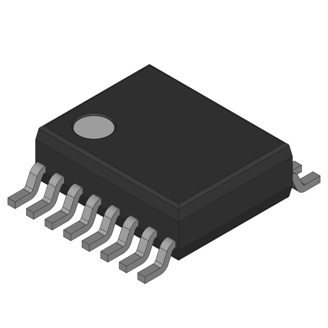
| 产品图片 |
|
| rohs | 符合RoHS无铅 / 符合限制有害物质指令(RoHS)规范要求 |
| 产品系列 | 接口 IC,数字隔离器,Analog Devices ADUM7510BRQZiCoupler® |
| 数据手册 | |
| 产品型号 | ADUM7510BRQZ |
| PulseWidthDistortion(Max) | 5ns |
| 上升/下降时间(典型值) | 2.5ns, 2.5ns |
| 产品种类 | |
| 传播延迟tpLH/tpHL(最大值) | 40ns, 40ns |
| 传播延迟时间 | 40 ns |
| 供应商器件封装 | 16-QSOP |
| 共模瞬态抗扰度(最小值) | 10kV/µs |
| 包装 | 管件 |
| 商标 | Analog Devices |
| 安装风格 | SMD/SMT |
| 封装 | Tube |
| 封装/外壳 | 16-SSOP(0.154",3.90mm 宽) |
| 封装/箱体 | QSOP-16 |
| 工作温度 | -40°C ~ 105°C |
| 工厂包装数量 | 98 |
| 技术 | 磁耦合 |
| 数据速率 | 10Mbps |
| 最大工作温度 | + 105 C |
| 最大数据速率 | 10 Mb/s |
| 最小工作温度 | - 40 C |
| 标准包装 | 98 |
| 电压-电源 | 4.5 V ~ 5.5 V |
| 电压-隔离 | 1000Vrms |
| 电源电压-最大 | 5.5 V |
| 电源电压-最小 | 4.5 V |
| 电源电流 | 0.7 mA |
| 类型 | General Purpose |
| 系列 | ADUM7510 |
| 绝缘电压 | 1 kVrms |
| 脉宽失真(最大) | 5ns |
| 视频文件 | http://www.digikey.cn/classic/video.aspx?PlayerID=1364138032001&width=640&height=505&videoID=2219593469001http://www.digikey.cn/classic/video.aspx?PlayerID=1364138032001&width=640&height=505&videoID=2219593470001http://www.digikey.cn/classic/video.aspx?PlayerID=1364138032001&width=640&height=505&videoID=2219614223001 |
| 输入-输入侧1/输入侧2 | 5/0 |
| 通道数 | 5 |
| 通道数量 | 5 Channel |
| 通道类型 | 单向 |
| 隔离式电源 | 无 |


- 商务部:美国ITC正式对集成电路等产品启动337调查
- 曝三星4nm工艺存在良率问题 高通将骁龙8 Gen1或转产台积电
- 太阳诱电将投资9.5亿元在常州建新厂生产MLCC 预计2023年完工
- 英特尔发布欧洲新工厂建设计划 深化IDM 2.0 战略
- 台积电先进制程称霸业界 有大客户加持明年业绩稳了
- 达到5530亿美元!SIA预计今年全球半导体销售额将创下新高
- 英特尔拟将自动驾驶子公司Mobileye上市 估值或超500亿美元
- 三星加码芯片和SET,合并消费电子和移动部门,撤换高东真等 CEO
- 三星电子宣布重大人事变动 还合并消费电子和移动部门
- 海关总署:前11个月进口集成电路产品价值2.52万亿元 增长14.8%


PDF Datasheet 数据手册内容提取
5-Channel, 1 kV Unidirectional Digital Isolator Data Sheet ADuM7510 FEATURES FUNCTIONAL BLOCK DIAGRAM RoHS-compliant, 16-lead, QSOP package Low power operation: 5 V VDD1 1 ADuM7510 16VDD2 1.2 mA per channel maximum @ 0 Mbps to 2 Mbps GND1 2 15 GND2 2.8 mA per channel maximum @ 10 Mbps VIA 3 ENCODE DECODE 14 VOA High temperature operation: 105°C VIB 4 ENCODE DECODE 13 VOB Up to 10 Mbps data rate (NRZ) VIC 5 ENCODE DECODE 12 VOC Low default output state VID 6 ENCODE DECODE 11 VOD 1Sa0f0e0t yV arnmds riesoglualtaitoonr yra atpinpgr ovals (pending) GNVDIE1 87 ENCODE DECODE 190 VGONED2 07632-001 UL recognition Figure 1. 1000 V rms for 1 minute per UL 1577 APPLICATIONS General-purpose, unidirectional, multichannel isolation GENERAL DESCRIPTION The ADuM75101 is a unidirectional 5-channel isolator based on interfaces and stable performance characteristics. The need for the Analog Devices, Inc., iCoupler® technology. In contrast to external drivers and other discrete components is eliminated with the ADuM1510, the ADuM7510 has a lower isolation rating, these iCoupler products. Furthermore, iCoupler devices run at offering a reduced cost option for applications that can accept one-tenth to one-sixth the power consumption of optocouplers a 1 kV ac isolation. Combining high speed CMOS and monolithic at comparable signal data rates. air core transformer technology, these isolation components The ADuM7510 isolator provides five independent isolation provide outstanding performance characteristics superior to channels supporting data rates up to 10 Mbps. Each side operates alternatives such as optocoupler devices. with the supply voltage of 4.5 V to 5.5 V. Unlike other optocoupler By avoiding the use of LEDs and photodiodes, iCoupler devices alternatives, the ADuM7510 isolator has a patented refresh eliminate the design difficulties commonly associated with opto- feature that ensures dc correctness in the absence of input logic couplers. The typical optocoupler concerns regarding uncertain transitions and during power-up/power-down conditions. current transfer ratios, nonlinear transfer functions, and temperature and lifetime effects are eliminated with the simple iCoupler digital 1 Protected by U.S. Patents 5,952,849; 6,873,065; and 7,075,329. Rev. B Information furnished by Analog Devices is believed to be accurate and reliable. However, no responsibility is assumed by Analog Devices for its use, nor for any infringements of patents or other One Technology Way, P.O. Box 9106, Norwood, MA 02062-9106, U.S.A. rights of third parties that may result from its use. Specifications subject to change without notice. No license is granted by implication or otherwise under any patent or patent rights of Analog Devices. Tel: 781.329.4700 www.analog.com Trademarks and registered trademarks are the property of their respective owners. Fax: 781.461.3113 ©2010–2012 Analog Devices, Inc. All rights reserved.
ADuM7510 Data Sheet TABLE OF CONTENTS Features .............................................................................................. 1 Absolute Maximum Ratings ............................................................5 Applications ....................................................................................... 1 ESD Caution...................................................................................5 Functional Block Diagram .............................................................. 1 Pin Configuration and Function Descriptions ..............................6 General Description ......................................................................... 1 Typical Performance Characteristics ..............................................7 Revision History ............................................................................... 2 Applications Information .................................................................8 Specifications ..................................................................................... 3 Printed Circuit Board (PCB) Layout ..........................................8 Electrical Characteristics—5 V Operation................................ 3 Propagation Delay-Related Parameters ......................................8 Package Characteristics ............................................................... 4 DC Correctness and Magnetic Field Immunity..............................8 Insulation and Safety-Related Specifications ............................ 4 Power Consumption .....................................................................9 Recommended Operating Conditions ...................................... 4 Power-Up/Power-Down Considerations ...................................9 Regulatory Information ............................................................... 4 Outline Dimensions ....................................................................... 10 Ordering Guide .......................................................................... 10 REVISION HISTORY 2/12—Rev. A to Rev. B Created Hyperlink for Safety and Regulatory Approvals Entry in Features Section ................................................................. 1 Change to Printed Circuit Board (PCB) Layout Section ............ 8 1/10—Revision A: Initial Version Rev. B | Page 2 of 12
Data Sheet ADuM7510 SPECIFICATIONS ELECTRICAL CHARACTERISTICS—5 V OPERATION All voltages are relative to their respective ground. 4.5 V ≤ V ≤ 5.5 V, 4.5 V ≤ V ≤ 5.5 V; all minimum/maximum specifications apply DD1 DD2 over the entire recommended operation range, unless otherwise noted; all typical specifications are at T = 25°C, V = V = 5 V. A DD1 DD2 Table 1. Parameter Symbol Min Typ Max Unit Test Conditions/Comments DC SPECIFICATIONS Input Quiescent Supply Current per Channel I 0.4 0.7 mA DDI (Q) Output Quiescent Supply Current per Channel I 0.3 0.5 mA DDO (Q) Total Supply Current, Five Channels1 V Supply Current, Quiescent I 2.0 3.5 mA V = V = V = V = V = 0 V DD1 DD1 (Q) IA IB IC ID IE V Supply Current, Quiescent I 1.5 2.5 mA V = V = V = V = V = 0 V DD2 DD2 (Q) IA IB IC ID IE V Supply Current, 10 Mbps Data Rate I 7.7 10 mA 5 MHz logic signal frequency DD1 DD1 (10) V Supply Current, 10 Mbps Data Rate I 3.3 4.0 mA 5 MHz logic signal frequency DD2 DD2 (10) Input Currents I , I , I , I , I −10 +1 +10 µA V , V , V , V , V ≥ 0 V IA IB IC ID IE IA IB IC ID IE Logic High Input Threshold V 2.0 V IH Logic Low Input Threshold V 0.8 V IL Logic High Output Voltages V , V , V − 0.4 4.8 V I = −4 mA, V = V OAH OBH DD2 Ox Ix IH V , V , OCH ODH V OEH Logic Low Output Voltages V , V , 0.2 0.4 V I = +4 mA, V = V OAL OBL Ox Ix IL V , V , V OCL ODL OEL SWITCHING SPECIFICATIONS Minimum Pulse Width2 PW 100 ns C = 15 pF, CMOS signal levels L Maximum Data Rate3 10 Mbps C = 15 pF, CMOS signal levels L Propagation Delay4 t , t 20 27 40 ns C = 15 pF, CMOS signal levels PHL PLH L Pulse-Width Distortion, |t − t |4 PWD 5 ns C = 15 pF, CMOS signal levels PLH PHL L Change vs. Temperature 5 ps/°C C = 15 pF, CMOS signal levels L Propagation Delay Skew5 t 30 ns C = 15 pF, CMOS signal levels PSK L Channel-to-Channel Matching6 t 5 ns C = 15 pF, CMOS signal levels PSKCD L Output Rise/Fall Time (10% to 90%) t /t 2.5 ns C = 15 pF, CMOS signal levels R F L Common-Mode Transient Immunity at |CM | 10 15 kV/µs V = V /V , V = 1000 V, H Ix DD1 DD2 CM Logic High Output7 transient magnitude = 800 V Common-Mode Transient Immunity at |CM| 10 15 kV/µs V = 0 V, V = 1000 V, L Ix CM Logic Low Output7 transient magnitude = 800 V Refresh Rate f 1.2 Mbps r Input Dynamic Supply Current per Channel8 I 0.14 mA/Mbps DDI (D) Output Dynamic Supply Current per Channel8 I 0.045 mA/Mbps DDO (D) 1 Supply current values are for all five channels combined, running at identical data rates. Output supply current values are specified with no output load present. The supply current associated with an individual channel, operating at a given data rate, can be calculated as described in the Power Consumption section. See Figure 4 through Figure 6 for information on the per-channel supply current as a function of the data rate for unloaded and loaded conditions. See Figure 7 and Figure 8 for total I and I supply currents as a function of the data rate for the ADuM7510. DD1 DD2 2 The minimum pulse width is the shortest pulse width at which the specified pulse width distortion is guaranteed. Operation below the minimum pulse width is not recommended. 3 The maximum data rate is the fastest data rate at which the specified pulse width distortion is guaranteed. 4 t propagation delay is measured from the 50% level of the falling edge of the V signal to the 50% level of the falling edge of the V signal. t propagation delay is PHL Ix Ox PLH measured from the 50% level of the rising edge of the V signal to the 50% level of the rising edge of the V signal. Ix Ox 5 t is the magnitude of the worst-case difference in t and/or t that is measured between units at the same operating temperature, supply voltages, and output PSK PHL PLH load within the recommended operating conditions. 6 Channel-to-channel matching is the absolute value of the difference in propagation delays between any two channels within the same component. 7 CM is the maximum common-mode voltage slew rate that can be sustained while maintaining V > 0.8 V × V . CM is the maximum common-mode voltage slew H O DD2 L rate that can be sustained while maintaining V < 0.8 V. The common-mode voltage slew rates apply to both rising and falling common-mode voltage edges. The O transient magnitude is the range over which the common mode is slewed. 8 Dynamic supply current is the incremental amount of supply current required for a 1 Mbps increase in the signal data rate. See Figure 4 through Figure 6 for infor- mation on the per-channel supply current as a function of the data rate for unloaded and loaded conditions. See the Power Consumption section for guidance on calculating the per-channel supply current for a given data rate. Rev. B | Page 3 of 12
ADuM7510 Data Sheet PACKAGE CHARACTERISTICS Table 2. Parameter Symbol Min Typ Max Unit Test Conditions/Comments Resistance (Input-to-Output)1 R 1012 Ω I-O Capacitance (Input-to-Output)2 C 2.2 pF f = 1 MHz I-O Input Capacitance2 C 4.0 pF I IC Junction-to-Ambient Thermal Resistance, QSOP θ 76 °C/W Thermocouple located at center of JA package underside 1 The device is considered a 2-terminal device. Pin 1 through Pin 8 are shorted together, and Pin 9 through Pin 16 are shorted together. 2 Input capacitance is from any input data pin to ground. INSULATION AND SAFETY-RELATED SPECIFICATIONS Table 3. Parameter Symbol Value Unit Test Conditions/Comments Rated Dielectric Insulation Voltage 1000 V rms 1 minute duration Minimum External Air Gap QSOP Package (Clearance) L(I01) 3.8 min mm Measured from input terminals to output terminals, shortest distance through air Minimum External Tracking QSOP Package (Creepage) L(I02) 3.8 min mm Measured from input terminals to output terminals, shortest distance path along body Tracking Resistance (Comparative Tracking Index) CTI >400 V DIN IEC 112/VDE 0303 Part 1 Isolation Group II Material Group (DIN VDE 0110, 1/89, Table 1) Maximum Working Voltage Compatible with 50 Years V 354 V peak Continuous peak voltage across the isolation barrier IORM Service Life RECOMMENDED OPERATING CONDITIONS All voltages are relative to their respective ground. See the DC Correctness and Magnetic Field Immunity section for information on immunity to external magnetic fields. Table 4. Parameter Symbol Min Max Unit Operating Temperature T −40 +105 °C A Supply Voltages V , V 4.5 5.5 V DD1 DD2 Input Signal Rise and Fall Times 1.0 ms REGULATORY INFORMATION The ADuM7510 is approved by the organization listed in Table 5. Table 5. UL (Pending) Recognized under UL 1577 component recognition program1 Single/basic insulation, 1000 V rms isolation voltage File E214100 1 In accordance with UL 1577, each ADuM7510 is proof tested by applying an insulation test voltage of 1200 V rms for 1 sec (current leakage detection limit = 5 µA). Rev. B | Page 4 of 12
Data Sheet ADuM7510 ABSOLUTE MAXIMUM RATINGS Ambient temperature T = 25°C, unless otherwise noted. A Stresses above those listed under Absolute Maximum Ratings may cause permanent damage to the device. This is a stress Table 6. rating only; functional operation of the device at these or any Parameter Rating other conditions above those indicated in the operational Storage Temperature (T ) Range −65°C to +150°C ST section of this specification is not implied. Exposure to absolute Ambient Operating Temperature (T ) −40°C to +105°C Range A maximum rating conditions for extended periods may affect Supply Voltages1 (V , V ) −0.5 V to +7.0 V device reliability. DD1 DD2 Input Voltages1 −0.5 V to V + 0.5 V DDI (V , V , V , V , V ) IA IB IC ID IE ESD CAUTION Output Voltages1 −0.5 V to V + 0.5 V DDO (V , V , V , V , V ) OA OB OC OD OE Average Output Current per Pin2 Side 1 (I ) −10 mA to +10 mA O1 Side 2 (I ) −10 mA to +10 mA O2 Common-Mode Transients3 −100 kV/μs to +100 kV/μs 1 All voltages are relative to their respective ground. 2 See Figure 3 for maximum rated current values for various temperatures. 3 Refers to common-mode transients across the insulation barrier. Common- mode transients exceeding the absolute maximum ratings may cause latch- up or permanent damage. Rev. B | Page 5 of 12
ADuM7510 Data Sheet PIN CONFIGURATION AND FUNCTION DESCRIPTIONS VDD1 1 16 VDD2 GND1* 2 15 GND2* VIA 3 ADuM7510 14 VOA VIB 4 TOP VIEW 13 VOB VIC 5 (Not to Scale) 12 VOC VID 6 11 VOD VIE 7 10 VOE GND1* 8 9 GND2* *PTCIOON N G2N NAEDNC1DT I ESPD IRN. E C8CO AONRMNEME IECNNTTIDENERGDN B.A POLILTNYH 9 C TAOON NDGN NPEDICN2T I1ES5D RA. ERCCEOO NINMNTMEECERNTNIDNAEGLDL B.YOTH 07632-002 Figure 2. Pin Configuration Table 7. Pin Function Descriptions Pin No. Mnemonic Description 1 V Supply Voltage for Isolator Side 1 (4.5 V to 5.5 V). DD1 2 GND Ground 1. Ground reference for Isolator Side 1. Pin 2 and Pin 8 are internally connected, and connecting both 1 to GND is recommended. 1 3 V Logic Input A. IA 4 V Logic Input B. IB 5 V Logic Input C. IC 6 V Logic Input D. ID 7 V Logic Input E. IE 8 GND Ground 1. Ground reference for Isolator Side 1. Pin 2 and Pin 8 are internally connected, and connecting both 1 to GND is recommended. 1 9 GND Ground 2. Ground reference for Isolator Side 2. Pin 9 and Pin 15 are internally connected, and connecting both 2 to GND is recommended. 2 10 V Logic Output E. OE 11 V Logic Output D. OD 12 V Logic Output C. OC 13 V Logic Output B. OB 14 V Logic Output A. OA 15 GND Ground 2. Ground reference for Isolator Side 2. Pin 9 and Pin 15 are internally connected, and connecting both 2 to GND is recommended. 2 16 V Supply Voltage for Isolator Side 2 (4.5 V to 5.5 V). DD2 Table 8. Truth Table (Positive Logic) V V V V Ix DD1 DD2 Ox Input1, 2 State State Output1 Description High Powered Powered High Normal operation, data is high. Low Powered Powered Low Normal operation, data is low. X Unpowered Powered Low Input unpowered. Outputs return to input state within 1 µs of V power restoration. DD1 See the Power-Up/Power-Down Considerations section for more details. X Powered Unpowered High-Z Output unpowered. Output pins are in high impedance state. Outputs return to input state within 1 µs of V power restoration. DD2 1 V and V refer to the input and output signals of a given channel (A, B, C, D, or E). IX OX 2 X = don’t care. Rev. B | Page 6 of 12
Data Sheet ADuM7510 TYPICAL PERFORMANCE CHARACTERISTICS 350 1.6 A) 300 m 1.4 D ( A A) O 1.2 m 250 L RENT ( 200 L 15pF 1.0 R E U N 0.8 C N M 150 HA XIMU NT/C 0.6 A 100 E M RR 0.4 U C 50 D20.2 D I 00 25 A5M0BIENT7 T5EMPER1A00TURE(1°2C5) 150 175 07632-003 00 2 DAT4A RATE (Mb6ps) 8 10 07632-006 Figure 3. Thermal Derating Curve, Dependence of Safety-Limiting Values Figure 6. Typical I Supply Current per Channel vs. Data Rate DD2 with Case Temperature per DIN V VDE V 0884-10 (15 pF Output Load) 1.6 8 1.4 7 A) m1.2 6 NEL (1.0 mA) 5 CURRENT/CHAN00..86 I CURRENT (DD1 43 D10.4 2 D I 0.2 1 00 2 DAT4A RATE (Mb6ps) 8 10 07632-004 00 2 DAT4A RATE (Mb6ps) 8 10 07632-007 Figure 4. Typical I Supply Current per Channel vs. Data Rate Figure 7. Typical Total I Supply Current vs. Data Rate DD1 DD1 1.6 8 1.4 7 mA)1.2 mA) 6 NEL (1.0 OAD ( 5 N L A F H p I CURRENT/CDD2000...864 I CURRENT 15DD2 432 0.2 1 00 2 DAT4A RATE (Mb6ps) 8 10 07632-005 00 2 DAT4A RATE (Mb6ps) 8 10 07632-008 Figure 5. Typical I Supply Current per Channel vs. Data Rate Figure 8. Typical Total I Supply Current vs. Data Rate DD2 DD2 (No Output Load) (15 pF Output Load) Rev. B | Page 7 of 12
ADuM7510 Data Sheet APPLICATIONS INFORMATION PRINTED CIRCUIT BOARD (PCB) LAYOUT If the decoder receives no pulses for more than about 5 μs, the input side is assumed to be unpowered or nonfunctional, in which The ADuM7510 digital isolator requires no external interface case, the isolator output is forced to a default low state by the circuitry for the logic interfaces. Power supply bypassing is strongly watchdog timer circuit (see Table 8). recommended at the input and output supply pins (see Figure 9). Bypass capacitors are most conveniently connected between Pin 1 The limitation on the magnetic field immunity of the device is and Pin 2 for V and between Pin 15 and Pin 16 for V . The set by the condition in which induced voltage in the transformer DD1 DD2 capacitor value should be between 0.01 μF and 0.1 μF. The total receiving coil is sufficiently large to either falsely set or reset the lead length between both ends of the capacitor and the input decoder. The following analysis defines such conditions. The power supply pin should not exceed 10 mm. Bypassing between ADuM7510 is examined in a 4.5 V operating condition because it Pin 1 and Pin 8 and between Pin 9 and Pin 16 should also be represents the most susceptible mode of operation of this product. considered unless the ground pair on each package side is The pulses at the transformer output have an amplitude greater connected close to the package. than 1.5 V. The decoder has a sensing threshold of about 1.0 V, VDD1 VDD2 thereby establishing a 0.5 V margin in which induced voltages GND1 GND2 can be tolerated. The voltage induced across the receiving coil is VIA VOA VIB ADuM7510 VOB given by VIC VOC VID VOD V = (−dβ/dt)∑∏rn2; n = 1, 2, …, N GNVDIE1 VGONED2 07632-009 where: Figure 9. Recommended PCB Layout β is the magnetic flux density. r is the radius of the nth turn in the receiving coil. See the AN-1109 Application Note for board layout guidelines. n N is the number of turns in the receiving coil. PROPAGATION DELAY-RELATED PARAMETERS Given the geometry of the receiving coil in the ADuM7510 and Propagation delay is a parameter that describes the length of an imposed requirement that the induced voltage be, at most, time it takes for a logic signal to propagate through a component. 50% of the 0.5 V margin at the decoder, a maximum allowable The propagation delay to a logic low output can differ from the magnetic field is calculated, as shown in Figure 11. propagation delay to a logic high output. 1000 INPUT (VIx) 50% UX FL 100 tPLH tPHL TIC OUTPUT (VOx) 50% 07632-010 MAGNE 10 Pulse width disFtiogrutrieo 1n0 .i Ps rtohpea gmataioxnim Duelmay Pdaifrfaemreentecrse between WABLE kgauss) 1 O( these two propagation delay values and is an indication of how LL 0.1 A accurately the input signal timing is preserved. M U M Channel-to-channel matching refers to the maximum amount XI 0.01 A M the propagation delay differs between channels within a single APrDopuaMga7t5i1o0n cdoemlapy osnkeewnt .r e fers to the maximum amount the 0.0011k 10kMAGNETI1C0 F0kIELD FREQ1MUENCY (Hz1)0M 100M 07632-011 Figure 11. Maximum Allowable External Magnetic Flux Density propagation delay differs among multiple ADuM7510 com- ponents operated under the same conditions. For example, at a magnetic field frequency of 1 MHz, the maximum allowable magnetic field of 0.5 kgauss induces DC CORRECTNESS AND MAGNETIC FIELD IMMUNITY a voltage of 0.25 V at the receiving coil. This is about 50% of the Positive and negative logic transitions at the isolator input sensing threshold and does not cause a faulty output transition. cause narrow (~1 ns) pulses to be sent via the transformer to If such an event occurs with the worst-case polarity during a the decoder. The decoder is bistable and is, therefore, either set transmitted pulse, it reduces the received pulse from >1.0 V to or reset by the pulses indicating input logic transitions. In the 0.75 V, still well above the 0.5 V sensing threshold of the absence of logic transitions at the input for more than ~1 μs, decoder. a periodic set of refresh pulses indicative of the correct input state are sent to ensure dc correctness at the output. Rev. B | Page 8 of 12
Data Sheet ADuM7510 The preceding magnetic flux density values correspond to specific For each output channel, the supply current is given by current magnitudes at given distances away from the ADuM7510 I = I f ≤ 0.5f DDO DDO (Q) r transformers. Figure 12 expresses these allowable current magni- I = (I + (0.5 × 10⁻³) × C × V ) × (2f − f) + I tudes as a function of frequency for selected distances. The DDO DDO (D) L DDO r DDO (Q) ADuM7510 is very insensitive to external fields. Only extremely f ≤ 0.5f r large, high frequency currents, very close to the component can where: potentially be a concern. For the 1 MHz example noted, a 1.2 kA I , I are the input and output dynamic supply currents DDI (D) DDO (D) current must be placed 5 mm away from the ADuM7510 to affect per channel (mA/Mbps). component operation. C is the output load capacitance (pF). L 1000 V is the output supply voltage (V). DDO f is the input logic signal frequency (MHz, half of the input data A) k rate, NRZ signaling). T ( 100 EN fr is the input stage refresh rate (Mbps). R UR IDDI (Q), IDDO (Q) are the specified input and output quiescent E C 10 supply currents (mA). L B A W To calculate the total IDD1 and IDD2 supply current, the supply O L 1 currents for each input and output channel corresponding to L A UM DISTANCE = 5mm IDD1 and IDD2 are calculated and totaled. Figure 4 and Figure 5 AXIM 0.1 DDIISSTTAANNCCEE == 110m0mm provide per-channel supply currents as a function of the data M rate for an unloaded output condition. Figure 6 provides per- channel supply current as a function of the data rate for a 15 pF 0.011k 10kMAGNETI1C0 F0kIELD FREQ1MUENCY (Hz1)0M 100M 07632-012 oIDuDt2p suutp cpolny dciutirornen. tF aigsu ar efu 7n acntido nF iogfu trhee 8 d partoa vriadtee tfootra Al IDDDu1M an7d5 10 Figure 12. Maximum Allowable Current for products. Various Current to ADuM7510 Spacings POWER-UP/POWER-DOWN CONSIDERATIONS Note that at combinations of strong magnetic field and high frequency, any loops formed by PCB traces can induce The ADuM7510 behaves as specified in Table 8 during power- sufficiently large error voltages to trigger the thresholds of up and power-down operations. However, the part can transfer succeeding circuitry. Take care to avoid PCB structures that incorrect data when the power supplies are below the minimum form loops. operating voltage but the internal circuits are not completely off. POWER CONSUMPTION Power-up/power-down errors can occur at V voltage near DDx the operating threshold of 1.9 V. The encoder generates data The supply current at a given channel of the ADuM7510 pulses at low amplitude. The detector can miss data pulses that isolator is a function of the supply voltage, the channel are near the detection threshold. If the transferring state is a data rate, and the channel output load. logic high, the encoder generates a pair of pulses; the decoder For each input channel, the supply current is given by can reject one of the pulses for low amplitude. A single pulse is IDDI = IDDI (Q) f ≤ 0.5fr interpreted as a logic low, and the output can be placed in the wrong logic state for that refresh cycle. I = I × (2f − f) + I f > 0.5f DDI DDI (D) r DDI (Q) r Glitch-free operation is possible by following these recommendations. Slew the power on or off as quickly as possible. Use the default low operating mode by holding the inputs low until power is stable. Rev. B | Page 9 of 12
ADuM7510 Data Sheet OUTLINE DIMENSIONS 0.197(5.00) 0.193(4.90) 0.189(4.80) 16 9 0.158(4.01) 0.154(3.91) 0.150(3.81) 0.244(6.20) 1 0.236(5.99) 8 0.228(5.79) 0.010(0.25) 0.020(0.51) 0.065(1.65) 0.069(1.75) 0.006(0.15) 0.010(0.25) 0.049(1.25) 0.053(1.35) 0.010(0.25) CO0P.0L0A4N(0A.1R0I)TY 0.02B5S(C0.64) 0.012(0.30) SPELAATNIENG 80°° 0.050(1.27) R0.E04F1(1.04) 0.004(0.10) 0.016(0.41) 0.008(0.20) COMPLIANTTOJEDECSTANDARDSMO-137-AB C(RINOEFNPEATRRREOENNLCLTEIHNEOGSNDELISYM)AEANNRDSEIAORRNOESUNANORDETEDAIN-POIPNFRFCOHINPECRSHI;AMTEEQILUFLOIIVMRAELUTEESNRETDISNIMFDOEERNSSIGIONN.S 01-28-2008-A Figure 13. 16-Lead Shrink Small Outline Package [QSOP] (RQ-16) Dimensions shown in inches and (millimeters) ORDERING GUIDE Number Number Maximum Maximum of Inputs, of Inputs, Maximum Propagation Pulse Width Temperature Package Package Model1, 2 V Side V Side Data Rate Delay, 5 V Distortion Range Description Option DD1 DD2 ADuM7510BRQZ 5 0 10 Mbps 40 ns 5 ns −40°C to +105°C 16-Lead QSOP RQ-16 ADuM7510BRQZ-RL7 5 0 10 Mbps 40 ns 5 ns −40°C to +105°C 16-Lead QSOP RQ-16 1 Z = RoHS Compliant Part. 2 RL7 = 7” tape and reel option. Rev. B | Page 10 of 12
Data Sheet ADuM7510 NOTES Rev. B | Page 11 of 12
ADuM7510 Data Sheet NOTES ©2010–2012 Analog Devices, Inc. All rights reserved. Trademarks and registered trademarks are the property of their respective owners. D07632-0-2/12(B) Rev. B | Page 12 of 12